DOI:
10.1039/B915205A
(Paper)
J. Mater. Chem., 2010,
20, 152-158
Morphology-controlled two-dimensional elliptical hemisphere arrays fabricated by a colloidal crystal based micromolding method†
Received
27th July 2009
, Accepted 18th September 2009
First published on
14th October 2009
Abstract
In this paper, we demonstrate a facile modified micromolding method to fabricate morphology-controlled elliptical hemisphere arrays (EHAs) by using stretched poly(dimethylsiloxane) (PDMS) nanowell arrays as molds. The PDMS nanowell arrays were fabricated via casting PDMS prepolymer onto two-dimensional (2D) non-close-packed (ncp) colloidal sphere arrays. By varying the stretching direction, stretching force, size of the colloidal spheres used and other experimental conditions in the fabrication process, we can control the shape, aspect ratio and size of the resulting microstructures. Moreover, our method does not involve any costly micromanufacture technique and can be applied to a great many materials, such as oil soluble polymers (e.g. polystyrene (PS)), water soluble polymers (e.g. poly(vinyl pyrrolidone) (PVP)), cross-linked polymers (e.g. photopolymerizable resin) and a variety of composites (e.g. polymer/nanoparticle composite). The anisotropic wetting properties of these EHAs were demonstrated. Potential application of the EHAs is to provide a model for the fundamental research of anisotropic surfaces and a template or mask for the fabrication of anisotropic surface patterns for potential applications of shape-dependent optical and magnetic devices.
Introduction
Surface-patterned micro- and nanostructures have attracted great attention for a wide range of applications in microelectronic and optoelectronic devices,1–4 as well as biological and chemical sensors.5,6 Many lithography methods for patterning surfaces in the micrometre and sub-micrometre ranges have been developed, including photolithography, electron beam lithography, X-ray lithography, scanning probe lithography,7–11 however, most of these traditional methods require expensive equipment and suffer from the disadvantage of being time-consuming. Compared to these traditional methods, self-assembly of colloidal spheres has been demonstrated to be another strategy which is inexpensive, simple to implement, inherently parallel and high-throughput.12–19 Based on this concept, a number of methods, which are now called colloidal lithography (CL), have been reported for fabricating two-dimensional (2D) or three-dimensional (3D) functional patterns, such as honeycomb patterns,2 ordered porous films,20 macroporous materials,21,22 and arrays of rings, cones, and columns.23–26 Since the self-assembled colloidal crystals in CL are usually built up by spheres, there still remains a challenge in this field, that is how to fabricate non-spherical arrays, which are more attractive in applications such as photonic crystals than their spherical counterparts due to their lower symmetries.27
Among all non-spherical arrays, elliptical arrays have been investigated for years because of their anisotropic properties.28–31 Although a number of methods have been successfully demonstrated for generating elliptical colloids with well-controlled sizes, shapes and in relatively large quantities,32–39 it is still very difficult to organize these elliptical building blocks into ordered arrangements over large areas. To overcome this problem, a new strategy has been proposed, which transfers ordered spherical arrays to non-spherical arrays by the utilization of light-induced deformation or mold-induced deformation. Through a linearly polarized Ar+ laser single-beam irradiation, stretching deformation of azo polymer colloidal spheres can be caused along the polarization direction of the laser beam,40 but owing to the close packing of the colloidal spheres the aspect ratio of the as-prepared colloidal elliptical spheres is limited by the interspace. By using deformed spherical arrays as molds elliptical arrays have been synthesized41–45 through the micromolding method, which is compatible with a broad range of materials and is capable of generating nano-scale features over large wafers,46–50 however, there still remains some disadvantages such as difficulty or high cost to fabricate 2D elliptical arrays, which are in need not only for fundamental research of anisotropic surfaces but also as templates or masks for the fabrication of other anisotropic surface arrays. Therefore, the development of facile, low-cost, and effective strategies for controllable fabrication of 2D elliptical arrays is urgently expected in potential applications of shape-dependent optical and magnetic devices.
Recently, we have reported the utilization of 2D non-close packed (ncp) colloidal crystals to mold poly(dimethylsiloxane) (PDMS) with hemispherical microwell arrays on a surface.51 In this paper, we present the utilization of the stretched 2D PDMS nanowell arrays as the original mold to fabricate micro- and sub-micrometre 2D elliptical hemisphere arrays (EHAs). The morphology of the arrays can be adjusted by changing the experimental conditions in the micromolding process, and a great many materials, ranging from thermoplastic polymers to thermosetting polymers, can be used in this strategy. Additionally, the desired anisotropic characteristics of these as-prepared arrays were studied by contact angle measurements. The main practical purpose of this work is to develop a facile, low-cost, and effective strategy leading to the fabrication of 2D elliptical arrays for both fundamental research and further application.
Experimental section
Materials
Silicon and glass substrates were cleaned by immersion in piranha solution (3:1 concentrated H2SO4/30% H2O2) for 1 h at 70 °C to create a hydrophilic surface and then rinsed repeatedly with Milli-Q water (18.2 MΩ cm−1) and ethanol. The substrates were dried in nitrogen gas before use. The silica microspheres were prepared by the Stöber method,52 and their sizes were measured at about 1115 nm, 576 nm and 237 nm by SEM with a calibrated length. PDMS elastomer kits (Sylgard 184) were purchased from Dow Corning (Midland, MI). Poly(vinyl alcohol) (PVA, Mw = 13![[thin space (1/6-em)]](https://www.rsc.org/images/entities/char_2009.gif) 000–23 ∼000), poly(vinyl pyrrolidone) (PVP, Mw = 360
000–23 ∼000), poly(vinyl pyrrolidone) (PVP, Mw = 360![[thin space (1/6-em)]](https://www.rsc.org/images/entities/char_2009.gif) 000), polystyrene (PS, Mw = 280
000), polystyrene (PS, Mw = 280![[thin space (1/6-em)]](https://www.rsc.org/images/entities/char_2009.gif) 000) and trichloro(1H,1H,2H,2H-perfluorooctyl) silane (PFS) were all purchased from Aldrich. (E)-9,9′-(4,4′-(but-1-en-3-yne-1,4-diyl)bis(4,1-phenylene)) bis(9H-carbazole) (CPEY) was purchased from Jilin Oled Material Technology company. The CdTe nanocrystal solution was prepared as reported earlier.53 A PVA (Mw = 13
000) and trichloro(1H,1H,2H,2H-perfluorooctyl) silane (PFS) were all purchased from Aldrich. (E)-9,9′-(4,4′-(but-1-en-3-yne-1,4-diyl)bis(4,1-phenylene)) bis(9H-carbazole) (CPEY) was purchased from Jilin Oled Material Technology company. The CdTe nanocrystal solution was prepared as reported earlier.53 A PVA (Mw = 13![[thin space (1/6-em)]](https://www.rsc.org/images/entities/char_2009.gif) 000–23
000–23![[thin space (1/6-em)]](https://www.rsc.org/images/entities/char_2009.gif) 000) solution (10 wt%) and CdTe nanocrystal solution (1.25 × 10⁻² M) was mixed 1 : 1 and the mixture was used to fabricate PVA/CdTe nanocrystal composite EHA. The photoresist oligomer comprises phthalic diglycol diacrylate (C22H26O10, PDDA), trimethylolpropane triacrylate (C15H20O6, TMPTA), epoxy acrylate oligomer (EA), and α- hydroxy isobutyryl benzene (C10H12O2, photoinitiator 1173). To prepare the TiO2 sol, titanium butoxide (4 mL) was mixed with 2-propanol (2 mL). After 15 min of stirring, a mixture of hydrochloric acid (17 µL), H2O (0.305 g) and 2-propanol (4 mL) was added dropwise to the stirring solution. The sol was stirred for 12 h and filtered with a 0.45 mm filter before use. The four components of the photoresist, Sulfuric acid, hydrogen peroxide, PVA (Mw = 71
000) solution (10 wt%) and CdTe nanocrystal solution (1.25 × 10⁻² M) was mixed 1 : 1 and the mixture was used to fabricate PVA/CdTe nanocrystal composite EHA. The photoresist oligomer comprises phthalic diglycol diacrylate (C22H26O10, PDDA), trimethylolpropane triacrylate (C15H20O6, TMPTA), epoxy acrylate oligomer (EA), and α- hydroxy isobutyryl benzene (C10H12O2, photoinitiator 1173). To prepare the TiO2 sol, titanium butoxide (4 mL) was mixed with 2-propanol (2 mL). After 15 min of stirring, a mixture of hydrochloric acid (17 µL), H2O (0.305 g) and 2-propanol (4 mL) was added dropwise to the stirring solution. The sol was stirred for 12 h and filtered with a 0.45 mm filter before use. The four components of the photoresist, Sulfuric acid, hydrogen peroxide, PVA (Mw = 71![[thin space (1/6-em)]](https://www.rsc.org/images/entities/char_2009.gif) 000), toluene and n-heptane were used as received.
000), toluene and n-heptane were used as received.
Preparation
2D ncp colloidal monolayers of silica spheres were prepared as reported earlier.54 The molds were prepared by casting PDMS prepolymer diluted in n-heptane (PDMS prepolymer:n-heptane = 1:5) onto the microsphere-covered substrates in order to impregnate in the interspace of the microspheres with PDMS prepolymer completely. After the pre-casted prepolymer was treated under vacuum (0.09 MPa) for 1 h to remove the entrained gas, another layer of PDMS prepolymer was casted on it. To facilitate the peeling off process, the silica template was pre-modified by PFS. Subsequently, the PDMS molds were cured in a conventional drying oven at 60 °C for 3 h. After being peeled off, the PDMS molds were stretched to a certain extent and then compressed onto a substrate coated with a film of PS with different thickness ranging from 11 nm to 310 nm and treated in a conventional drying oven at 130 °C for 3 h. Finally, when cooled to room temperature the PDMS molds were peeled off from the substrate and the PS EHAs were left on the substrate. The PS/CPEY composite and PVP EHAs were synthesized following the method described above. The PVA/Rhodamine B composite and PVA/CdTe nanocrystal composite EHAs were fabricated by compressing the stretched mold onto the substrate coated with a thin film of aqueous solution of the composite and then peeling off the mold after the solvent evaporated. Photopolymerizable resin EHAs were obtained by compressing the stretched mold onto the substrate coated with a thin oligomer film and peeling off the mold after UV exposure. TiO2 EHAs were prepared by compressing the stretched mold onto the substrate coated with a thin film of TiO2 sol and peeling off the mold after the evaporation of the solvent. Samples were heated to 450 °C at a rate of 10 °C per min and held at 450 °C for 30 min to convert the TiO2 to the anatase form.
Characterization
Atomic force microscopy (AFM) images were recorded in tapping mode with a Nanoscope IIIa scanning probe microscope from Digital Instruments under ambient conditions. Scanning electron microscopy (SEM) micrographs were taken with a JEOL FESEM 6700F electron microscope with primary electron energy of 3 kV. Before imaging, the samples with polymer structures were sputter-coated with 2 nm of Pt. Water droplets of 3 µl were used for the contact angle (CA) measurements. All of the measurements were performed at room temperature using a drop shape analysis system (DSA 10 MK2, KRÜSS). At least 5 measurements were averaged for all of the data reported here. Fluorescent photo images were taken with an Olympus fluorescence microscope (BX51).
Results and discussion
Formation of 2D elliptical hemispheres arrays
PDMS molds with 2D nanowell arrays.
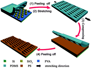
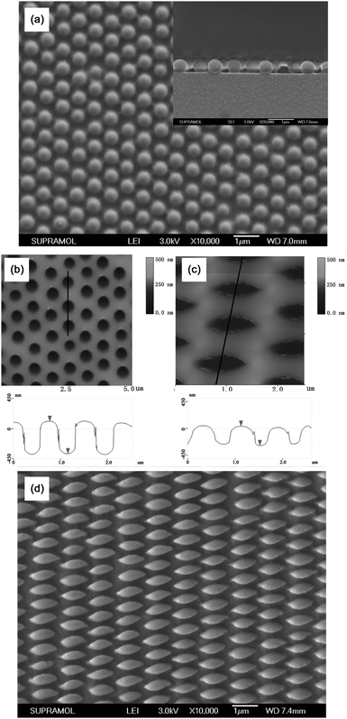
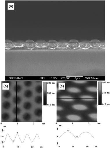
Fig. 1 outlines the procedures for the fabrication of 2D PS EHAs. Monodispersed silica spheres with average diameter (D) of 576 nm were taken as an example to illustrate the fabrication process. Firstly, 2D hexagonal ncp colloidal monolayers of silica spheres were fabricated on PVA-coated substrate by using lift-up soft lithography and solvent-swelling.54 As can be seen in the SEM image (Fig. 2a), the silica spheres keep the original hexagonal arrangement with increased lattice space (1.49D). Moreover, because the spheres sank into the PVA film during the transfer process, the ncp structure of the sphere arrays is mechanically stable, and the average height of the exposed silica spheres is about 474 nm as shown in the inset of Fig. 2a. After pouring the PDMS prepolymer onto the microsphere-covered substrates and peeling off the PDMS mold after curing, we could obtain the PDMS molds, which possessed patterned hemispherical nanowells in a hexagonal ncp lattice. The AFM image of the nanowell array is shown in Fig. 2b. The lattice spacing of the obtained crystal structure is also about 1.49D and the average depth of the formed nanowells is about 433 nm, which indicates that the highly ordered hexagonal ncp arrangement of the silica spheres is preserved.
 |
| | Fig. 1 A schematic illustration for the fabrication of 2D EHAs using PDMS nanowells as the molds. | |
 |
| | Fig. 2 (a) SEM image of 2D hexagonal ncp silica spheres on the PVA-covered substrate. The inset is the cross-section SEM. (b) AFM image (top) and line profile (down) of 2D hexagonal ncp nanowells on the PDMS mold fabricated by using silica spheres as the template. The sphere interstices are 0.49D. (c) AFM image (top) and line profile (down) of the stretching deformed 2D hexagonal ncp nanowells under a certain force. (d) SEM image of the obtained 2D EHA of PS on the silicon wafer. | |
2D elliptical hemisphere array of PS.
Elliptical nanowells were obtained via stretching the as-prepared PDMS nanowell molds to a certain extent, and the AFM image of the stretched mold is shown in Fig. 2c. As can be seen in the AFM image, the average length of the nanowells increased to 938 nm, while the depth and the width of the nanowells decreased to 323 nm and 279 nm compared with the original dimension (418 nm in length and width, 433 nm in depth) owing to the shrinkage along the two directions perpendicular to the stretching direction. The stretched PDMS nanowell mold was then compressed onto a silicon substrate coated with PS film under a certain pressure and heated to a temperature over the glass transition temperature (Tg) of PS for a period of time (3 hours). Because of the movement of PS under heat and pressure, 2D PS EHA was obtained as shown in Fig. 2d. The AFM image (Fig. S1, ESI†) shows that the dimensions of the elliptical hemispheres all correspond well with those of the stretched PDMS nanowells. Because of the elasticity of PDMS, the elliptical mold recovered to the round mold after the force used to stretch the PDMS mold was unloaded, which means that the PDMS are reusable. In order to obtain well developed EHAs, the pre-coated PS film must be thick enough to be filled in the nanowells completely. The optimized thickness is over 140 nm for nanowell molds peeled off from the 578 nm silica spheres template. The AFM images of the resulting microstructures are shown in Fig. S2 (ESI†) by varying the thickness of the PS films. If the thickness is just a little less than 140 nm, due to the template effect of the mold, the PS EHAs can also form with a lower height compared with the well developed hemispheres, but a much thinner film may result in the formation of random embossment. In this paper, we chose a PS film with a thickness of 140 nm to fabricate the EHAs using nanowells peeled off from the 576 nm silica template.
Morphology-controlled fabrication of the EHAs
Effects of the stretching direction on the morphology of the elliptical hemispheres.
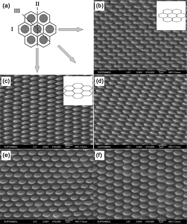
As illustrated in Fig. 3a, in 2D hexagonal arrays each sphere belongs to a hexagon area, and there are two types of symmetry axis (I and II) crossing two opposite sides and two vertices, respectively, therefore the stretching direction can affect the stress distribution around each nanowell and further affect the morphology of the elliptical hemispheres formed from the deformed nanowells. Fig. 3b, 3c and 3d show the SEM images of EHAs obtained when stretching the PDMS nanowell mold along the direction of I, II and III, respectively. In the case of I, because of the shrinkage along the diagonal line of the hexagon area and the increase of the distance between two opposite sides (inset of Fig. 3b), the formed elliptical hemisphere has a smooth edge and the shape of the hemispheres is a transition state from round to rectangle (Fig. 3b). When the mold was stretched along direction II, owing to the stretching of the diagonal line (inset of Fig. 3c), the formed elliptical hemispheres have two sharp cusps at each apex of the long axis and the ellipses are rhomb-like, as shown in Fig. 3c. Additionally, when the stretching directions are not along the two types of symmetry axis, especially when stretching along direction III, the stress distribution is not symmetrical around the nanowell, which induces the asymmetry shape of the obtained hemispheres, and the formed hemispheres are more like parallelograms than ellipses (Fig. 3d). EHAs with ellipses bigger than the size of the original silica template can also be obtained when stretching the mold along one direction and preventing the shrinkage of the mold along the perpendicular direction (Fig. 3e and 3f). Additionally, in our experiment, the size of arrays with homogeneous structured could be larger than 100 µm2 with some dot and line defects, as shown in Fig. S3 (ESI†).
 |
| | Fig. 3 (a) A schematics illustration of three typical stretching direction of hexagonal arrangement of nanowells. (b), (c) and (d) show the SEM images of the obtained 2D PS EHAs on the silicon wafer when stretching along direction I, II and III, respectively. The inset of (b) and (c) shows the schematic lattice model of hexagonal arrays after being stretched along direction I and II, respectively. (e) and (f) are SEM images of EHAs obtained via stretching along direction I and II while keeping the mold along another direction, respectively. | |
Stretching force dependence of the aspect ratio of the ellipse.
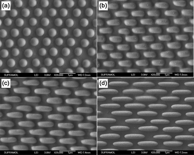
Through changing the force applied to stretch the PDMS nanowell arrays to form the elliptical nanowell, the aspect ratio of the obtained EHAs can be adjusted in a certain range (from 1 to 3.63). Fig. 4 shows the SEM images of the obtained arrays using different forces to stretch the PDMS nanowell mold. When no force was applied, the hemispheres are round (Fig. 4a), and the diameter of the hemisphere was 524 nm (well in accordance with the diameter of the silica spheres used to fabricate the PDMS mold). When the force was about 0.3 N, the nanowell deformed just a bit, the long axis and short axis of the obtained EHAs changed to about 824 nm and 380 nm, and the aspect ratio was about 2.16 (Fig. 4b). When the force was increased to about 0.6 N, the long axis and short axis of the obtained EHAs changed further to about 1020 nm and 356 nm, and the aspect ratio of the formed hemispheres increased to about 2.87 (Fig. 4c); The aspect ratio of the ellipse increased to 3.63 when the PDMS mold was stretched under a force (0.9 N) just a bit less than the breaking force of the mold (Fig. 4d). We believe that the aspect ratio can be further increased when using more elastic PDMS.
 |
| | Fig. 4 SEM images of obtained hemispheres arrays when the stretching force was (a) 0 N, (b) 0.3 N, (c) 0.6 N and (d) 0.9 N. | |
EHAs with tunable height.
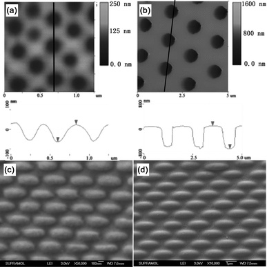
As shown above, the height of the EHA fits well with the elliptical nanowell mold peeled off from the silica array template, thus, the height of the EHAs can be adjusted by altering the thickness of the PVA film used to immobilize the silica spheres. The cross-section SEM image of the silica spheres template fabricated using the PVA solution with a concentration of 5 wt% is shown in Fig. 5a. It is shown that most of the silica spheres are sunk into the PVA films, and that the height of the exposed silica spheres above the PVA film is about 177 nm resulting in the depth of the PDMS nanowell mold peeled off from this silica template being about 137 nm, as shown in the AFM images (Fig. 5b). Furthermore, the height of the PS elliptical hemispheres decreased to about 120 nm as shown in the AFM image (Fig. 5c) of the PS EHA formed using the PDMS nanowell mold fabricated using a PVA solution with a higher concentration. Additionally, Fig. S4 (ESI†) presents the plot data of the height of the exposed silica spheres measured by SEM (Fig. S5, ESI†) against the concentration of the PVA solution used to fabricate the silica template, which indicates that the depth of the PDMS nanowells can be tuned from 137 nm to 433 nm. That is to say the height of the EHAs can be adjusted from 120 nm to 323 nm.
 |
| | Fig. 5 (a) Cross section SEM image of the ncp silica arrays sank into PVA film when using the PVA aqueous solution with a concentration of 5 wt%. (b) and (c) show the AFM images (top) and line profiles (down) of the as-prepared PDMS nanowell arrays and the PS EHA using the silica template of (a). | |
EHAs with tunable size.
By adjusting the diameter of the colloidal sphere template, EHAs with tunable sizes can also be fabricated. Fig. 6a and 6b are the AFM images of PDMS molds peeled off from the 237 nm and 1115 nm ncp silica templates, respectively, and as shown, the average depth of the obtained wells is 87 nm and 743 nm, respectively. Additionally, via stretching the PDMS mold using a stretching force of 0.6 N, EHAs with different sizes can also be fabricated on the substrate (Fig. 6c and 6d). The aspect ratios of the ellipses obtained using PDMS molds peeled off from the 237 nm and 1115 nm ncp silica templates are 2.68 and 2.71, respectively, fitting well with that of the ellipse obtained from the 576 nm silica template using the same force. This result indicates that the aspect ratio of the ellipse is independent of the feature size of the nanostructures, and may be adjusted by changing the macroscopic stretching extent of the PDMS nanowell molds.
 |
| | Fig. 6 (a) and (b) show the AFM image (top) and line profile (down) of the PDMS nanowells molds peeled off from the silica spheres template with diameters of 237 nm and 1115 nm, respectively. (c) and (d) are the SEM images of EHAs fabricated using the PDMS molds of (a) and (b), respectively. | |
Fabrication of EHAs of other materials
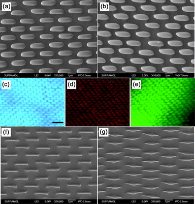
By changing the chemical composition of the material and controlling the experimental condition, we could obtain EHAs with different chemical compositions. Fig. 7a and 7b are the SEM images of the as-prepared water soluble polymer (PVP) and cross-linked polymer (photopolymerizable resin) EHAs using the 1115 nm silica spheres array as the original template, respectively. Furthermore, EHAs of a variety of composites can also be fabricated using the stretched PDMS nanowell molds. Fig. 7c, 7d and 7e show the fluorescent photo images of EHAs fabricated using oil soluble composite (PS/CPEY composite), water soluble composite (PVA/Rhodamine B composite) and organic/inorganic composite (PVA/CdTe nanocrystal composite), respectively, and the original template was also the 1115 nm silica spheres array. As indicated in the fluorescent microscopy micrographs, the fluorescence properties were preserved well after the micromolding process. Because TiO2 sol is flowable and it is easy for the TiO2 sol to be filled in the elliptical wells, inorganic TiO2 elliptical arrays can also been fabricated through using sol–gel method, however, because of the shrinkage during the calcination process, the as-prepared ellipses have a shorter short axis and lower height which is not defined only by the size of the elliptical PDMS wells, as shown in Fig. 7f and 7g.
 |
| | Fig. 7 (a) and (b) are SEM images of EHAs of PVP and photopolymerizable resin, respectively. (c), (d) and (e) are the fluorescent photo images of EHAs of PS/CPEY composite, PVA/Rhodamine B composite and PVA/CdTe nanocrystal composite, respectively. Scale bar represents 5 µm. (f) and (g) are the SEM images of the obtain TiO2 elliptical array fabricated through using the sol–gel method. | |
Anisotropy wetting character of these as-prepared EHAs
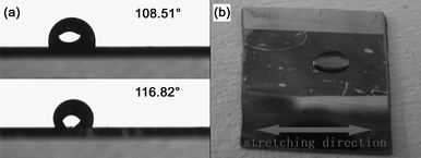
Since the surface morphology could influence the surface characteristics significantly, the as-prepared elliptical surface structure may have anisotropic properties. The wetting behavior of a water drop on the as-prepared surface was studied as a representative of the anisotropic character of the EHAs. Fig. 8a shows the cross-sectional shapes of a 3 µL water drop from two orthogonal directions perpendicular and parallel to the long axis direction on the surface with the EHA of PS fabricated using the 576 nm silica template and a stretching force of 0.6 N. As shown in Fig. 8a, we found that the static contact angles (CA) measured from the direction parallel to the long axis were larger than those measured from the perpendicular direction. Because the period of the EHAs along the long axis is bigger than that along the short axis, thus the energy barriers that the system must overcome when the three-phase contact line moves along the long axis are less than that along the short axis, and it is the difference of the energy barriers that induces the difference in the CA values of two orthogonal directions.55 The anisotropic wetting property is like the wetting property of rice leaf reported before,56 but it is worthwhile to point out that the anisotropic wetting property in our experiment is induced by the sub-micro elliptical structures rather than the strip structure in tens of micrometres in the case of rice leaf. Furthermore, by exposing the EHAs in the oxygen plasma for just a few seconds to make the surface a little more hydrophilic, the anisotropic wetting property can be well illustrated by the morphology of a 3 µL water drop on the EHA (Fig. 8b), because the wetting property of the materials can further affects the anisotropic extent of wetting, the anisotropic extent increases as the hydrophilicity of the material used increases.
 |
| | Fig. 8 (a) Side views of a sessile drop on the surface from perpendicular (top) and parallel (bottom) to the direction of the stretching direction, respectively. (b) Optical photograph of a 3 µL water drop on the EHAs. | |
Conclusions
In summary, we have succeeded in fabricating elliptical hemisphere arrays via a micromolding approach using stretched PDMS nanowells as molds. Moreover, the morphology of the elliptical nanostructures can be controlled by tuning the stretching force applied, the thickness of the PVA film of the original silica templates and other treatment conditions. The wetting behavior of the water drop exhibits the anisotropic character of the as-prepared EHAs. As our strategy does not involve in any costly fabrication techniques and can be applied to a great many polymers and a variety of polymer composites, we believe that the fabricated EHAs will show significant promise for further use for the fundamental research of anisotropic surfaces and fabrication of other elliptical arrays with unique properties, especially for the anisotropic property.
Acknowledgements
This work was supported by the National Natural Science Foundation of China (Grant Nos. 20534040, 20874039, 20921003) and the National Basic Research Program of China (2007CB936402).
Notes and references
- J. G. Veinot, H. Yan, S. M. Smith, J. Cui, Q. Huang and T. J. Marks, Nano Lett., 2002, 2, 333 CrossRef CAS.
- C. L. Haynes and R. P. V. Duyne, J. Phys. Chem. B, 2001, 105, 5599 CrossRef CAS.
- M. Behl, J. Seekamp, S. Zankovych, C. M. S. Torres, R. Zentel and J. Ahopelto, Adv. Mater., 2002, 14, 588 CrossRef CAS.
- M. C. McAlpine, R. S. Friedman and C. M. Lieber, Nano Lett., 2003, 3, 443 CrossRef CAS.
- H. Q. Shi, W. B. Tsai, M. D. Garrison, S. Ferrari and B. D. Ratner, Nature, 1999, 398, 593 CrossRef CAS.
- Y. Cui, Q. Q. Wei, H. K. Park and C. M. Leiber, Science, 2001, 293, 1289 CrossRef CAS.
- Y. N. Xia, J. A. Rogers, K. E. Paul and G. M. Whitesides, Chem. Rev., 1999, 99, 1823 CrossRef CAS.
- D. Y. Khang, H. Yoon and H. H. Lee, Adv. Mater., 2001, 13, 749 CrossRef CAS.
- G. M. Wallraff and W. D. Hinsberg, Chem. Rev., 1999, 99, 1801 CrossRef CAS.
- M. Kahl, E. Voges, S. Kostrewa, C. Viets and W. Hill, Sens. Actuators, B, 1998, 51, 285 CrossRef.
- T. W. Ebbesen, H. J. Lezec, H. F. Ghaemi, T. Thio and P. A. Wolff, Nature, 1998, 391, 667 CrossRef CAS.
- M. E. Abdelsalam, P. N. Bartlett, J. J. Baumberg and S. Coyle, Adv. Mater., 2004, 16, 90 CrossRef CAS.
- F. Sun, W. Cai, Y. Li, B. Cao, Y. Lei and L. Zhang, Adv. Funct. Mater., 2004, 14, 283 CrossRef CAS.
- Y. H. Cho, G. Cho and J. S. Lee, Adv. Mater., 2004, 16, 1814 CrossRef CAS.
- J. E. Barton and T. W. Odom, Nano Lett., 2004, 4, 1525 CrossRef CAS.
- Y. Lu, H. Xiong, X. Jiang, Y. Xia, M. Prentiss and G. M. Whitesides, J. Am. Chem. Soc., 2003, 125, 12724 CrossRef CAS.
- J. M. McLellan, M. Geissler and Y. Xia, J. Am. Chem. Soc., 2004, 126, 10830 CrossRef CAS.
- D. G. Choi, H. K. Yu, S. G. Jang and S. M. Yang, J. Am. Chem. Soc., 2004, 126, 7019 CrossRef CAS.
- P. Jiang, Angew. Chem., Int. Ed., 2004, 43, 5625 CrossRef CAS.
- B. Cao, W. Cai, F. Sun, Y. Li, Y. Lei and L. Zhang, Chem. Commun., 2004, 1604 RSC.
- O. D. Velev, T. A. Jede, R. F. Lobo and A. M. Lenhoff, Nature, 1997, 389, 447 CrossRef CAS.
- P. V. Braun and P. Wilzius, Nature, 1999, 402, 603 CrossRef CAS.
- Z. Sun, Y. Li, J. Zhang, Y. Li, Z. Zhao, K. Zhang, G. Zhang, J. Guo and B. Yang, Adv. Funct. Mater., 2008, 18, 4036 CrossRef CAS.
- H. L. Chen, S. Y. Chuang, C. H. Lin and Y. H. Lin, Opt. Express, 2007, 15, 14793 CrossRef.
- X. Zhang, J. Zhang, Z. Ren, X. Li, X. Zhang, D. Zhu, T. Wang, T. Tian and B. Yang, Langmuir, 2009, 25, 7375 CrossRef CAS.
- S. G. Jang, H. K. Yu, D. G. Choi and S. M. Yang, Chem. Mater., 2006, 18, 6103 CrossRef CAS.
- Y. Yin and Y. Xia, Adv. Mater., 2001, 13, 267 CrossRef CAS.
- I. Guedes, M. Grimsditch, V. Metlushko, P. Vavassori, R. Camley, B. Ilic, P. Neuzil and R. Kumar, Phys. Rev. B: Condens. Matter Mater. Phys., 2003, 67, 024428 CrossRef.
- F. J. Castaño, C. A. Ross and A. Eilez, J. Phys. D: Appl. Phys., 2003, 36, 2031 CrossRef CAS.
- J. M. Oran, R. J. Hinde, N. A. Hatab, S. T. Retter and M. J. Sepaniak, J. Raman Spectrosc., 2008, 39, 1811 CrossRef CAS.
- J. Elliott, I. I. Smolyaninov, N. I. Zheludev and A. V. Zayats, Opt. Lett., 2004, 29, 1414 CrossRef.
- S. P. Sutera and C. W. Boylan, J. Colloid Interface Sci., 1980, 73, 295 CrossRef CAS.
- K. M. Keville, E. I. Franses and J. M. Caruthers, J. Colloid Interface Sci., 1991, 144, 103 CrossRef CAS.
- M. Nagy and A. Keller, Polym. Commun., 1989, 30, 130 CAS.
- M. Ocaña, M. P. Morales and C. J. Serna, J. Colloid Interface Sci., 1995, 171, 85 CrossRef CAS.
- J. A. Champion, Y. K. Katare and S. Mitragotri, Proc. Natl. Acad. Sci. U. S. A., 2007, 104, 11901 CrossRef CAS.
- Y. Hu, J. Ge, T. Zhang and Y. Yin, Adv. Mater., 2008, 20, 4599 CrossRef CAS.
- E. Snoeks, A. van Blaaderen, T. van Dillen, C. M. van Kats, M. L. Brongersma and A. Polman, Adv. Mater., 2000, 12, 1511 CrossRef CAS.
- Y. Lu, Y. Yin and Y. Xia, Adv. Mater., 2001, 13, 271 CrossRef CAS.
- Y. Li, Y. He, X. Tong and X. Wang, Langmuir, 2006, 22, 2288 CrossRef CAS.
- Y. Lu, Y. Yin, Z. Li and Y. Xia, Langmuir, 2002, 18, 7722 CrossRef CAS.
- L. Ji, J. Rong and Z. Yang, Chem. Commun., 2003, 1080 RSC.
- Z. Y. Xie, L. G. Sun, G. Z. Han and Z. Z. Gu, Adv. Mater., 2008, 20, 3601 CrossRef CAS.
- Y. Zhang, E. A. Matsumoto, A. Peter, P. C. Lin, R. D. Kamien and S. Yang, Nano Lett., 2008, 8, 1192 CrossRef CAS.
- B. Pokroy, A. K. Epstein, M. C. M. Persson-Gulda and J. Aizenberg, Adv. Mater., 2009, 21, 463 CrossRef CAS.
- J. Gao, Y. Liu, H. Xu, Z. Wang and X. Zhang, Langmuir, 2009, 25, 4365 CrossRef CAS.
- N. L. Jeon, I. S. Choi, B. Xu and G. M. Whitesides, Adv. Mater., 1999, 11, 946 CrossRef CAS.
- H. Mĺguez, N. Tétreault, S. M. Yang, V. Kitaev and G. A. Ozin, Adv. Mater., 2003, 15, 597 CrossRef CAS.
- Z. Y. Cheng, Z. Wang, R. B. Xing, Y. C. Han and J. Lin, Chem. Phys. Lett., 2003, 376, 481 CrossRef CAS.
- M. L. Kovarik, N. J. Torrence, D. M. Spence and R. Scott Martin, Analyst, 2004, 129, 400 RSC.
- Z. Ren, X. Li, J. Zhang, W. Li, X. Zhang and B. Yang, Langmuir, 2007, 23, 8272 CrossRef CAS.
- W. Stöber, A. Fink and E. Bohn, J. Colloid Interface Sci., 1968, 26, 62 CrossRef.
- H. Zhang, L. Wang, H. Xiong, L. Hu, B. Yang and W. Li, Adv. Mater., 2003, 20, 1712 CrossRef.
- X. Yan, J. M. Yao, G. Lu, X. Li, J. H. Zhang, K. Han and B. Yang, J. Am. Chem. Soc., 2005, 127, 7688 CrossRef CAS.
- Y. Zhao, Q. Lu, M. Li and X. Li, Langmuir, 2007, 23, 6212 CrossRef CAS.
- L. Feng, S. Li, Y. Li, H. Li, L. Zhang, J. Zhai, Y. Song, B. Liu, L. Jiang and D. Zhu, Adv. Mater., 2002, 14, 1857 CrossRef CAS.
Footnote |
| † Electronic Supplementary Information (ESI) available: AFM images of the microstructures with varying thicknesses of the PS films, SEM images of EHA fabricated stretching along direction I with low magnification, the height of the exposed silica spheres against the concentration of the PVA solution used to fabricate the silica template, cross-section SEM images of the silica template fabricated using PVA solution with different concentrations. See DOI: 10.1039/b915205a/ |
|
| This journal is © The Royal Society of Chemistry 2010 |
Click here to see how this site uses Cookies. View our privacy policy here. ![[thin space (1/6-em)]](https://www.rsc.org/images/entities/char_2009.gif) 000–23 ∼000), poly(vinyl pyrrolidone) (PVP, Mw = 360
000–23 ∼000), poly(vinyl pyrrolidone) (PVP, Mw = 360![[thin space (1/6-em)]](https://www.rsc.org/images/entities/char_2009.gif) 000), polystyrene (PS, Mw = 280
000), polystyrene (PS, Mw = 280![[thin space (1/6-em)]](https://www.rsc.org/images/entities/char_2009.gif) 000) and trichloro(1H,1H,2H,2H-perfluorooctyl) silane (PFS) were all purchased from Aldrich. (E)-9,9′-(4,4′-(but-1-en-3-yne-1,4-diyl)bis(4,1-phenylene)) bis(9H-carbazole) (CPEY) was purchased from Jilin Oled Material Technology company. The CdTe nanocrystal solution was prepared as reported earlier.53 A PVA (Mw = 13
000) and trichloro(1H,1H,2H,2H-perfluorooctyl) silane (PFS) were all purchased from Aldrich. (E)-9,9′-(4,4′-(but-1-en-3-yne-1,4-diyl)bis(4,1-phenylene)) bis(9H-carbazole) (CPEY) was purchased from Jilin Oled Material Technology company. The CdTe nanocrystal solution was prepared as reported earlier.53 A PVA (Mw = 13![[thin space (1/6-em)]](https://www.rsc.org/images/entities/char_2009.gif) 000–23
000–23![[thin space (1/6-em)]](https://www.rsc.org/images/entities/char_2009.gif) 000) solution (10 wt%) and CdTe nanocrystal solution (1.25 × 10⁻² M) was mixed 1 : 1 and the mixture was used to fabricate PVA/CdTe nanocrystal composite EHA. The photoresist oligomer comprises phthalic diglycol diacrylate (C22H26O10, PDDA), trimethylolpropane triacrylate (C15H20O6, TMPTA), epoxy acrylate oligomer (EA), and α- hydroxy isobutyryl benzene (C10H12O2, photoinitiator 1173). To prepare the TiO2 sol, titanium butoxide (4 mL) was mixed with 2-propanol (2 mL). After 15 min of stirring, a mixture of hydrochloric acid (17 µL), H2O (0.305 g) and 2-propanol (4 mL) was added dropwise to the stirring solution. The sol was stirred for 12 h and filtered with a 0.45 mm filter before use. The four components of the photoresist, Sulfuric acid, hydrogen peroxide, PVA (Mw = 71
000) solution (10 wt%) and CdTe nanocrystal solution (1.25 × 10⁻² M) was mixed 1 : 1 and the mixture was used to fabricate PVA/CdTe nanocrystal composite EHA. The photoresist oligomer comprises phthalic diglycol diacrylate (C22H26O10, PDDA), trimethylolpropane triacrylate (C15H20O6, TMPTA), epoxy acrylate oligomer (EA), and α- hydroxy isobutyryl benzene (C10H12O2, photoinitiator 1173). To prepare the TiO2 sol, titanium butoxide (4 mL) was mixed with 2-propanol (2 mL). After 15 min of stirring, a mixture of hydrochloric acid (17 µL), H2O (0.305 g) and 2-propanol (4 mL) was added dropwise to the stirring solution. The sol was stirred for 12 h and filtered with a 0.45 mm filter before use. The four components of the photoresist, Sulfuric acid, hydrogen peroxide, PVA (Mw = 71![[thin space (1/6-em)]](https://www.rsc.org/images/entities/char_2009.gif) 000), toluene and n-heptane were used as received.
000), toluene and n-heptane were used as received.
