Metal surface nucleated supercritical fluid–solid–solid growth of Si and Ge/SiOx core–shell nanowires†
Christopher A.
Barrett
a,
Robert D.
Gunning
a,
Thomas
Hantschel
b,
Kai
Arstila
b,
Catriona
O'Sullivan
a,
Hugh
Geaney
a and
Kevin M.
Ryan
*a
aMaterials and Surface Science Institute and Department of Chemical and Environmental Sciences, University of Limerick, Limerick, Ireland. E-mail: kevin.m.ryan@ul.ie; Tel: +353 61213167
bInteruniversitair Micro-Elektronica Centrum, Kapeldreef 75, B-3001, Leuven, Belgium
First published on 3rd November 2009
Abstract
High yields of both single-crystalline Si and Ge/SiOx core–shell nanowires were nucleated and grown in metal reactor cells under high-pressure supercritical fluid conditions, without the addition of catalyst particle seeds or a porous template. Nanowire growth was only achieved when the fluid medium of supercritical CO2 and the organometallic precursors were used in conjunction with a coordinating solvent, trioctylphosphine. The diameter and length of the nanowires are found to be in the ranges of 30 to 60 nm and 1 to 10 µm, respectively. The correlation of nanowire growth with the eutectic binary phase diagrams of the semiconductor–metal and the presence of metal impurities at the base of the synthesized nanowires suggest a supercritical fluid–solid–solid growth mechanism occurring from the reaction cell walls. The nanowires are characterized by transmission electron microscopy, energy-dispersive X-ray spectroscopy, X-ray photoelectron spectroscopy and scanning electron microscopy. The electrical characteristics for individually picked nanowires are also investigated by means of mechanical nanoprobing.
Introduction
One-dimensional semiconductor nanostructures are attracting significant attention for application in next generation electronic and photonic devices.1 Their unique size-dependent electronic and optical properties2,3 have already resulted in their successful implementation in high-capacity power cells,4,5 field effect transistors6,7 and third generation solar cells.8,9 In the semiconductor industry, crystalline nanowires are sought as they offer thermodynamically stable features, are typically defect-free, single-crystalline and have a number of advantages over thin films in such applications as high-performance transistor arrays.10 Si and Ge nanowires have been of particular interest given their high compatibility with standard CMOS (complementary metal–oxide–semiconductor) technology and their expected ease of integration in future electronic devices.11 The more complex, core–shell nanowires of Ge/SiOx have also drawn considerable attention, with the higher intrinsic carrier mobilities of Ge to that of Si creating the ideal carrier channel and with the more insulating SiOx shell simplifying the chemical passivation of the structure compared to that of GeOx.12,13Si and Ge nanowires have been prepared by employing a variety of different techniques, such as laser ablation,14 physical thermal evaporation,15 chemical vapour deposition,16 and the more popular, vapour–liquid–solid (VLS).17,18 The VLS growth mechanism utilizes a metal catalyst seed particle (Au, Bi, Co, Cu, Ni, and Fe) to form a eutectic alloy droplet with the desired semiconductor material. Saturation of the alloy droplet with additional monomer leads to the extrusion of a one-dimensional semiconductor nanowire at reduced temperatures afforded by the eutectic alloy.19,20 Variations of VLS have been developed where monomer addition to the eutectic seed droplet can be provided from solution–liquid–solid (SLS)21 or from supercritical fluid–liquid–solid (SFLS)22 to realize anisotropic growth. One semiconductor integration issue that has been highlighted with these methods is the rapid diffusion of metal atoms from the alloy droplet into Si and Ge nanowires, decreasing the dielectric strength in addition to increasing p–n junction leakage.23,24
Supercritical fluids have been used to achieve non-seeded nanowire growth by infilling of porous templates, however, discrete single-crystalline nanowires are more difficult to obtain in this manner which is more suited to high-density array based applications.25 The sub-eutectic vapour–solid–solid (VSS) technique has been recently highlighted for the advantages offered through its reduced processing temperatures.26 Growth in this case proceeds in a similar fashion to that of VLS mechanism but at temperatures below the required melting points of the bulk eutectic alloy.27 The incorporation of unintentional impurities, particularly from the metal catalyst, may be reduced in VSS nanowires due to the reduction in atom diffusivity and solid solubility associated with nanowire growth at lower temperatures. The utilization of supercritical toluene, in the Ni nanocrystal seeded synthesis of Si and Ge nanowires, demonstrated growth by a solid phase seeding mechanism from the metal particle.28,29 Kamins et al. found that Si nanowire growth could occur in relatively high yields on flat Si surfaces without the addition of any seed particles.30 They showed that a CVD based solid-state diffusion of Si and Ti precursors could be used to create crystalline TiSi2 “nano-islands” which acted as nucleation points for anisotropic growth.31 Related studies have also shown that crystalline Ge nanowires could be grown from pure Fe substrates without the addition of structure-directing metal seeds, where again a diffusion process in the solid-state is the suggested mechanism.32
Recently we reported the formation of Si nanocrystals, where crystal growth was localized to the solution phase, affording the controlled evolution of pseudo-spherical to tetrahedral shaped nanocrystals.33 Here we demonstrate the supercritical fluid–solid–solid (SFSS) growth of single-crystal Si and Ge/SiOx nanowires from metal reactor sidewalls without the incorporation of particle seeds. Nanowire nucleation could be reproducibly achieved in a thermolysing fluid medium of supercritical CO2 using diphenyl-silane/germane precursors in conjunction with a coordinating solvent, trioctylphosphine. Nanowire growth is selective to the metal cell used, with anisotropic growth of Si occurring from stainless steel reaction vessels and not from titanium. Energy-dispersive X-ray (EDX) spectroscopy mapping is used to detect the presence of trace concentrations of metal at the bases of the nanowires, which is consistent with the type of reactor used in each case and confirms sidewall nucleation. The nanowires are typically over 1 µm in length and relatively defect-free throughout, as evidenced by high-resolution transmission electron microscopy (HRTEM) and high-resolution scanning electron microscopy (HRSEM). The electrical characteristics of the nanowires, as probed by a nanomanipulator, show a non-linear behaviour consistent with electron tunnelling through the experimentally observed surface oxide.
Experimental
Materials and apparatus
All chemicals were used as received unless otherwise stated. Diphenylsilane (DPS) (97%) and trioctylphosphine (TOP) (>90%) were received from Sigma-Aldrich and diphenylgermane (DPG) (97%) was supplied by Gelest, all of which were stored and dispensed from a nitrogen filled glove box. Experiments were conducted using liquid carbon dioxide (CO2) from BOC (99.85%) and the reaction cells, stainless steel tubing and connections were all supplied from High Pressure Equipment Co. The microreactors used were of a grade-2 titanium and 316 stainless steel construction, designed specifically for high temperatures and pressures. A Teledyne model 260D computer controlled syringe pump was used to pressurize the system and an Applied Test Systems Inc. model 3210, 3-zone heating furnace, was used to regulate temperature.Synthesis and purification
Nanowires were synthesized by thermal decomposition of DPG and DPS in the presence of TOP, at 650 °C and 4000 psi in supercritical carbon dioxide (sc-CO2). The reactions were carried out in 5 ml, high-pressure, stainless steel or titanium reaction cells. In a typical synthesis of Si nanowires, a stainless steel reaction cell was loaded with 400 µl of TOP and 500 µl of DPS under an inert atmosphere of a nitrogen filled glove box. For the synthesis of Ge/SiOx core–shell nanowires, 400 µl of TOP, 250 µl of DPS and 250 µl of DPG were loaded into a titanium reaction cell. All cells were sealed under nitrogen before removal and connected to the computer controlled syringe pump, using 1/8 inch stainless steel high-pressure tubing (see ESI†, Fig. S1). Using the syringe pump, liquid CO2 was pumped into a reaction cell and the pressure was increased above its critical point (Tc = 31 °C, Pc = 1030 psi) to 3000 psi. The 3-zone heating furnace was preheated to 665 °C, 15 °C above the required reaction temperature of 650 °C. At this point the reactor was placed in the furnace and would reach the desired temperature in under a minute. When the system had stabilized at the desired temperature, the pressure was further increased to 4000 psi. Both temperature and pressure were then kept constant for the proceeding reaction time of 30 min, at which point the furnace was opened and cooled to room temperature. CO2 was then vented from the reaction cell leaving a black powder residue.Chloroform was injected into the cell and subsequently removed to extract the nanowires from the reactor. All samples were initially centrifuged at 2000 rpm for 10 min to remove a precipitate, containing carbon by-products of the reaction. 10 ml of acetone were then added to the remaining solution of nanowires, followed by 2 min of light sonication. Samples were then centrifuged for 10 min at 5000 rpm, after which the solutions could be discarded and the remaining precipitate re-dispersed with 20 ml of a 1 : 1 mixture of acetone and chloroform. These steps were repeated twice more before the precipitate was again re-dispersed in 20 ml of chloroform for analysis. All samples were stored in glass vials within a nitrogen filled glove box to prevent against nanocrystal oxidation.
Characterization
The transmission electron microscopy (TEM) images of samples and the corresponding selected area electron diffraction (SAED) patterns were taken on a JEOL JEM-2011 electron microscope operated at an accelerating voltage of 200 kV using a LaB6 filament. Energy-dispersive X-ray (EDX) analysis was performed with a Princeton Gamma Tech Prism 1G system with a 10 mm2 Si detector and an Oxford Instruments INCAPentaFET-x3 system, with a Si(Li) detector and a 30 mm2 detecting crystal. X-Ray diffractograms were recorded on a Philips X'Pert PRO MPD (multi-purpose X-ray diffractometer), using a Cu-Kα radiation source and standard scintillation detector. XPS data were acquired using a KRATOS AXIS 165 X-ray photoelectron spectrometer equipped with a dual anode (Mg/Al) source and raster ion beam sputtering gun. The scanning electron microscopy (SEM) images of the as-synthesized samples were obtained by an FEI XL-30 system operated at 5 kV. Electrical transport measurements were performed in the FEI XL-30 SEM system using Kleindiek nanomanipulators of model MM3A-EM, allowing the positioning of independent probe tips with nanometre accuracy on individual nanowires while observing the process by SEM. The probes were electrochemically sharpened tungsten wires from Picoprobe of type T4, with a nominal tip radius of 100 nm. Current–voltage (I–V) curves were measured with the nanowires held at room temperature, using a programmable semiconductor test system (Keithley, model 4200SCS).Results and discussion
On completion of a typical Si nanowire synthesis, consecutive centrifugation and redispersion cleaning steps left a grey-black solution of nanowires which were relatively clean with no significant by-product observable. The Si nanowires were found to aggregate into large bundles, which settled out of solution after an hour, but could be readily re-dispersed by light sonication. Fig. 1a shows a SEM image of the Si nanowires, grown from stainless steel reactors, where yields of ∼30 mg of crystalline product could readily be obtained. Despite the gradual aggregation of the nanowires into larger intertwined bundles, discrete nanowires were found to have diameters between 10 and 50 nm and lengths greater than 1 µm. No visible luminescence was apparent from the chloroform dispersions of the nanowires, which would be expected given that the average diameter of the nanowires observed was larger than the Bohr excitation radius for Si (r = 4.9 nm). Small dark regions of an organic nature, observable under SEM, were found to decompose under the intensity of the beam upon close inspection. It is likely that residual surfactant of TOP and its oxide (trioctylphosphine oxide) would be still present in the sample and can be attributed to these organic areas. An investigation with pressure changes of ±1000 psi from the optimum conditions was conducted, with no large degree of effect on the resulting nanowire yield being found. However, lowering the reaction temperatures did reduce the overall yield in both cases, causing an increase in the relative amount of amorphous by-product formed. Decomposition of the sc-CO2 occurred readily at elevated reaction temperatures (>700 °C), which stifled the growth of any crystalline material. It was noted that in the absence of TOP from the system, under normal conditions, Si nanowire growth did not occur. Previous studies have shown that the addition of hydrocarbon ligands to sc-CO2 not only act as capping ligand for the subsequent nanocrystals formed but also attributes a degree of steric stabilization to emerging nuclei during the reaction, playing a crucial role to anisotropic growth.34,35 Sc-CO2 is also known to have a low degree of solvation, therefore we expect that the addition of TOP also acts to increase the availability of monomer in solution, sustaining wire growth.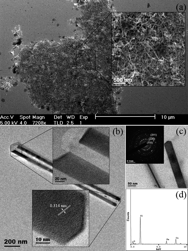 | ||
| Fig. 1 SEM image (a) from a dense area of Si nanowires collected from a stainless steel reaction vessel and a magnified view showing the intertwined nanowires (inset). TEM image (b) of Si nanowires with the corresponding HRTEM images, taken from either ends of the nanowires (inset). TEM image (c) of Si nanowires, with the corresponding polycrystalline diffraction pattern from several localized nanowires (inset). An EDX spectrum obtained from the spectroscopic analysis of the Si nanowires (d). | ||
Fig. 1b shows a TEM image of typical, as-synthesized Si nanowires that are approximately 1.5 µm in length and 45 nm in diameter. The HRTEM image from the tip of one of the Si nanowires (inset) shows visible lattice fringes from its single-crystalline structure with interplanar spacings of 0.314 nm. This is in good agreement with the d spacing of the [111] plane for diamond cubic crystalline Si. As is observable from the insets of Fig. 1b, a noticeable feature of the nanowires was that the base of each individual wire was found to be flat, however, the opposite end was usually more geometrically defined, owing to the faceted termination of crystal growth. This faceted tip at one end of the nanowires would seem to point towards solution-born nanocrystals, however, the flatter appearance of the diametrical end is more suggestive of the nanowires being nucleated and grown from a surface rather than in solution. It is likely that the flatter ends of these nanowires, coupled with their slight broader diameters, are the points at which a nanowire was cleaved from the nucleating metal surface. Although structure-directing particle seeds were not used, the size variation in nanowires was found to only range between 10 and 50 nm in diameter (Fig. 1c). The corresponding electron diffraction analysis (inset) shows a polycrystalline diffraction pattern, from which the maximum intensity of the diffraction rings gives d spacings of 0.313, 0.191 and 0.162 nm. These spacings can be matched to the lattice parameters of [111], [220] and [311] for the diamond cubic crystal structure of Si. EDX analysis from an area of high nanowire concentration is shown in Fig. 1d. An expected strong Si peak is observed with lower intensity peaks of O, C, Fe, and Cu also indicated. The copper and carbon peaks originate from the copper TEM grid and its amorphous carbon film support, while the minor oxygen peak can be attributed to native oxide formation along the Si nanowires. With no metal catalyst particles being added to the synthesis of the Si nanowires it can be assumed that the Fe detected in the nanowires is indicative that nucleation occurred from the sidewalls of the reactor given that this is the only source of Fe during the synthesis.
Furthering the study of Si nanowire growth from metal surfaces, a move from stainless steel to titanium reactor vessels was made, with all other reaction parameters unchanged. However, in the subsequent investigations with the Ti high-pressure cells, it was discovered that sidewall nucleation of Si nanowires did not occur under the same conditions. It is thought that higher temperatures would be necessary for anisotropic growth of crystalline Si to occur from Ti,36 which in this case, were found to be beyond the scope of the temperatures attainable with supercritical CO2. To overcome this barrier, a mixture of Si and Ge precursors was used in the reaction, so as to reduce the required nucleation temperature for nanowire growth. Ge offers the advantage of similar chemical properties to those of Si albeit with weaker binding energies, allowing crystal growth at much lower temperatures. Through the addition of DPG to the reaction system, in a 1 : 1 volume ratio with DPS, one-dimensional growth of the novel, core–shell nanostructures was achieved. At equivalent reaction temperatures and pressures, Ge/SiOx core–shell nanostructures, grown from titanium reaction cells, gave 30% more crystalline material per synthesis compared to the yields of pure Si nanowires. This can be attributed to the lower temperatures required for nano-crystalline Ge to be nucleated, leaving a smaller percentage of amorphous by-products to be removed. Fig. 2a shows a SEM image of a typical bundle of core–shell nanowires deposited from solution, where again co-deposition of TOP amongst the aggregated nanowires is further evident (inset).
![SEM image (a) from a high-density area of Ge/SiOx core–shell nanowires collected from a titanium reactor. TEM image (b) of Ge/SiOx core–shell nanowire with the corresponding HRTEM image (inset) showing visible lattice fringing from the Ge core. The corresponding single-crystal electron diffraction pattern (c), taken from the core–shell nanowire, where crystal growth is indexed for the [110] direction. An EDX spectrum obtained from the spectroscopic analysis of Ge/SiOx core–shell nanowires (d).](/image/article/2010/JM/b914950c/b914950c-f2.gif) | ||
| Fig. 2 SEM image (a) from a high-density area of Ge/SiOx core–shell nanowires collected from a titanium reactor. TEM image (b) of Ge/SiOx core–shell nanowire with the corresponding HRTEM image (inset) showing visible lattice fringing from the Ge core. The corresponding single-crystal electron diffraction pattern (c), taken from the core–shell nanowire, where crystal growth is indexed for the [110] direction. An EDX spectrum obtained from the spectroscopic analysis of Ge/SiOx core–shell nanowires (d). | ||
A more detailed analysis from discrete nanowires of the synthesis was carried out using HRTEM. The core–shell nanostructure in Fig. 2b can clearly be distinguished and consists of a crystalline germanium core (30 nm) surrounded by a thick layer of amorphous SiOx (30 nm). It is expected that this structure occurs due to the decomposition of DPG at lower temperatures to that of DPS, allowing the formation of Ge nanowires to occur initially, with subsequent encapsulation from the deposition of amorphous SiOx. This was confirmed through the omission of DPG from a typical synthesis, where XPS analysis found the epitaxial formation of SiOx across the Ti surface. It would seem that higher temperatures are required to produce the necessary surface diffusion of Si across Ti, in the anisotropic growth of Si nanowires. In the absence of this, it is thought that Si monomer, produced during the thermal decomposition of DPS, reacts with the surrounding sc-CO2 fluid, thus driving the epitaxial formation of amorphous SiOx. This was further observed when synthesis temperatures exceeding 700°C were used, where the complete oxidation of the precursor and the decomposition of sc-CO2 stifled the growth of crystalline material. The HRTEM image inset reveals the lattice fringing of the Ge core at the amorphous–crystalline boundary. Analysis from several nanowires found that growth occurred predominantly in the [110] direction with a smaller percentage of nanowires growing in the [111] direction. The corresponding selected area electron diffraction (Fig. 2c) indicates that the core is single-crystal Ge. The indexed Bragg reflections for this core–shell nanowire correspond to the [![[1 with combining macron]](https://www.rsc.org/images/entities/char_0031_0304.gif) 12] zone axis. Calculations for the rectangular pattern give a spacing of 0.327 and 0.198 nm, respectively, which can be indexed for the [111] and [220] directions of diamond cubic germanium with interplanar angles of 90°. From the larger lattice spacings seen from HRTEM and electron diffraction analysis, coupled with the fact that nucleation temperatures for Si1−xGex in a Si–Ge–Ti ternary isotherm exceed 900 °C, it is reasonable to assume that the core is composed of only single-crystal Ge. EDX analysis taken from a bundle of core–shell nanowires (Fig. 2d) shows a strong signal from the outer SiOx shell enclosing the nanowires with a lower intensity peak emerging from the inner Ge cores. It is expected that the degradation of TOP, added as a capping ligand for the nanowires, may cause a degree of doping in the semiconducting nanowires, evidence of which can be seen in the weak signal picked up from the presence of phosphorous in the sample.
12] zone axis. Calculations for the rectangular pattern give a spacing of 0.327 and 0.198 nm, respectively, which can be indexed for the [111] and [220] directions of diamond cubic germanium with interplanar angles of 90°. From the larger lattice spacings seen from HRTEM and electron diffraction analysis, coupled with the fact that nucleation temperatures for Si1−xGex in a Si–Ge–Ti ternary isotherm exceed 900 °C, it is reasonable to assume that the core is composed of only single-crystal Ge. EDX analysis taken from a bundle of core–shell nanowires (Fig. 2d) shows a strong signal from the outer SiOx shell enclosing the nanowires with a lower intensity peak emerging from the inner Ge cores. It is expected that the degradation of TOP, added as a capping ligand for the nanowires, may cause a degree of doping in the semiconducting nanowires, evidence of which can be seen in the weak signal picked up from the presence of phosphorous in the sample.
Fig. 3a shows an in situ HRSEM image of a Ge/SiOx core–shell nanowire grown from a Ti substrate, placed inside a reactor vessel during synthesis and an approaching tungsten tip from a nanomanipulator, used to mechanically sever the nanowires. The roots left behind after cleaving the nanowires (Fig. 3b) show typical cross-sections for core–shell nanostructures, where the conductive Ge core encircled in a SiOx shell is clearly defined. From SEM analysis, it was apparent that the nanowires were randomly nucleating from the surface of the titanium substrate. Nanowires were subsequently picked and placed onto carbon coated TEM grids, using a nanomanipulator. The high angle annular dark field (HAADF) STEM image, shown in Fig. 3c, gives a clear profile of a typical core–shell nanowire with a Ge crystalline core of 50 nm in diameter. A more extensive examination from the base of the core–shell nanowires revealed trace elements of Ti which was not originally detected. The EDX spectra (Fig. 3d and e) are taken from a line profile analysis along the breath of a Ge/SiOx core–shell nanowire, where signals for Si, O, Ge, Ti and P can be seen. Analysis was carried out at 3 separate segments along the core–shell nanowire. Ge was found to be localized to the core at each point along the nanowire, with the broader SiOx shell being detected across the full breath of the nanowire (see ESI†, Fig. S2). The presence of Ti is also identifiable, however, from the positional analysis it would appear that the inherent metal contamination is localized to the Ge core. This Ti signal was only found in one of the 3 scans, the scan positioned closests to the base of the nanowire and is expected to be as a result of Ti seeded growth of the crystalline Ge. Spectroscopic analysis from areas further along the core–shell nanowire did not reveal the presence of any Ti. However, the P signal was present at each location along the nanowire, which can be contributed to an expected alkyl phosphonic ligand functionalization. This is in good agreement with the assumption of Ge nanowires nucleating from the Ti substrate in the initial stages of the reaction and the subsequent deposition of SiOx occurring later.
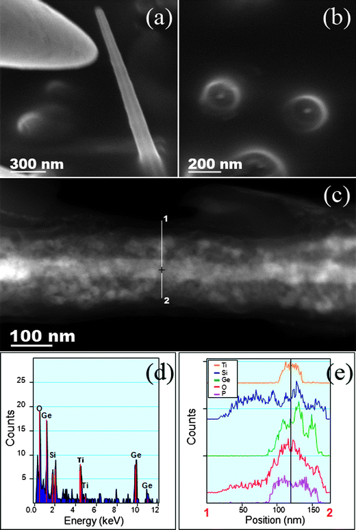 | ||
| Fig. 3 SEM image (a) of a Ge/SiOx core–shell nanowire being picked by a nanomanipulator and (b) cross-sectional image of the roots left behind. HAADF STEM image (c) showing a side profile of a picked core–shell nanowire. EDX spectra obtain from the line profile analysis of the Ge/SiOx nanowire (d and e). | ||
Nanowires were deposited from solution onto a Si wafer, where individual nanowires could be extracted from bundles for electrical characterization. Nanowires were plucked by slowly maneuvering a tungsten probe into a position of contact with the tip of the nanostructure, which was subsequently reinforced using localized carbon deposition (Fig. 4a). This carbon adhesion between tungsten probe and nanowire afforded a bond, strong enough to retract the probe along with the desired nanowire (Fig. 4b). A second probe could then be maneuvered into position at the opposite end of the nanowire to complete the circuit for transmission line analysis of current, measured by a picoammeter. In the electrical characterization experiments, a circuit was configured so that a potential difference could be applied between the tungsten probes connected at either end of a specific nanowire. The current–voltage sweeps plotted in Fig. 4c are measurements taken across individual Si and Ge/SiOx nanowires. The two-point probe measurements show non-linear transport, with the flow of current across the core–shell nanowires being several orders of magnitude lower than that of the Si nanowires. It is most likely that the core–shell nanowire suspended across the two probes (Fig. 4c, inset) can only make a physical contact through the SiOx shell. Electrical conduction is achieved by tunnelling through this insulating barrier causing the SiOx shell to dominate the electrical characteristics. The non-linear transport properties exhibited by the core–shell nanowires indicate an expected tunnelling effect through the amorphous SiOx layer. Similarly, the presence of a native oxide in the case of the Si nanowires, as well as an expected contact resistance between tungsten tip and nanowire, can explain the non-linearity observed in the current–voltage data. Using a Brinkmann fit,37 the insulating barrier was calculated at 4.8 and 53.2 nm for Si and Ge/SiOx nanowires, respectively, which is consistent with native oxide and the thickness range of 30 to 60 nm observed for the SiOx shell layers.
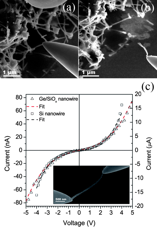 | ||
| Fig. 4 SEM image (a) of a tungsten tip approaching a Ge/SiOx nanowire and (b) the subsequent picking of the core–shell nanowire. Current–voltage graph (c) taken from individual Ge/SiOx (left y-axis) and Si (right y-axis) nanowires, suspended across two tungsten probes (inset) during electrical characterization. | ||
Several factors in the synthesis method reported here point towards a SFSS growth mechanism from the reactor sidewalls. The first of these is the characteristic faceted shape at one end of the nanowires and flat base at the diametrical end, in conjunction with the detection of trace amounts of metal atoms localized to the base of the nanowires, which can only have originated from the reactor cell walls. By contrast, nanowires which are grown from gold seeded SFLS systems are typically found to have a characteristic metal droplet at their end, which was not observed in any of the nanostructures synthesized in this study. Additionally, the lowest liquid eutectic in the bulk equilibrium phase diagrams of Ti/Ge and Fe/Si occurs at temperatures of 900 °C and 1200 °C, respectively. With the growth temperatures in this study being well below the bulk eutectic temperatures for each metal system, a solid seeding mechanism is the most likely route of formation. Given this it is reasonable to assume that the crystal growth during synthesis is diffusion controlled and would seem to explain the absence of Si nanowire nucleation from titanium surfaces. This can be explained by the rate of Si-based precursor decomposition, in combination with the subsequent reduced rate of monomer diffusion through Ti, being too low for anisotropic growth to occur, instead resulting in epitaxial formation. Fig. 5a shows a SEM image taken during the analysis of a stainless steel substrate, removed from a reactor after a typical synthesis of Si nanowires. Random anisotropic growth of Si nanowires can be clearly seen nucleating from the surface of the piece of metal. By increasing both the pressure conditions and the precursor loadings, higher densities of nanowires could be grown (see ESI†, Fig. S3). The magnified regions in the inset show that the nanowire diameters are in agreement with those observed from the nanowire bundles obtained upon extraction from the reaction cell (Fig. 1a). The selectivity of Si growth to the stainless steel is also of interest. It was found that in the diffusion process of the system, a high saturation of Si monomer within the steel reactor would lead to the formation of an iron silicide layer at the fluid–solid phase boundary. XPS analysis of the stainless steel coupons, placed within the reactors during synthesis, confirmed the diffusion of silicon into steel and the formation of a very thin layer of iron silicide across the exposed surface, which was not detected by XRD analysis (see ESI†, Fig. S4). It is suspected that this thin alloy film acts as a medium for Si, promoting anisotropic growth of Si nanowires from the cell walls by means of a solid-state diffusion process. Mathur et al. observed a similar process, where a thin alloy film mediated the growth of Ge nanowires from Fe substrates by means of a CVD based system.32
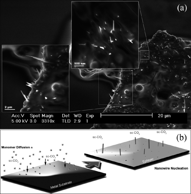 | ||
| Fig. 5 SEM image (a) taken from a steel substrate where Si nanowires can be seen grown from the metal surface. A schematic representation (b) showing the initial surface diffusion of silicon monomer leading to the nucleation of Si nanowires. | ||
Fig. 5b shows a representation of the nanowire growth process, where the thermolysis of the phenyl precursors in sc-CO2 is used to deliver high concentrations of monomer for subsequent diffusion into the surrounding metal surfaces. The intermediate transport properties of the supercritical fluid, in the presence of TOP, allow for a faster rate of monomer supply in diffusion limited reactions, compared to those of liquid based systems. Its higher densities also provide good solvation and thus increase reactant loadings as compared to gas-phase systems.38 The process of surface diffusion can be generally described as the motion of atoms or atomic clusters at solid material surfaces.39 Just as in bulk diffusion, this motion is typically a thermally promoted process, with rates increasing with increasing temperatures. The demonstrated nucleation and growth of nanowires from stainless steel and titanium surfaces are in good agreement with similar systems where diffusion behaviour leads to the formation of nano-crystalline domains, acting as nucleation sites for anisotropic growth.40 Close packed crystal lattices such as fcc [110] have higher diffusion rates, as well as increased electron and hole transport compared to the more open faces of fcc [100], resulting in the evolution of unique morphologies according to the differing crystallographic planes.41,42 These surface energy differences cause growth rate variations which are reflected in the predominant growth seen for nanowires in the [110] direction. From this, it is believed that a solid phase mechanism of growth for the nanostructures occurs at the base of the nanowires, where the metal concentrations were found to be at their highest. It is therefore expected that nanowire growth with supercritical fluids can occur for any semiconductor with a high solubility in the metal, however, the growth temperature must be sufficiently high for fast saturation by solid-state diffusion.
Conclusions
In summary, thermolysis of Si and Ge phenyl precursors in a sc-CO2 fluid medium generates a fast monomer saturation needed to drive diffusion into the reactor sidewalls, inducing nucleation of anisotropic Si or Ge/SiOx nanostructures. Structure-directing catalyst particles were not used, nor was any evidence of metal seed droplets found at the ends of the nanostructures. Given that the Fe and Ti were found localized to the base of the nanowires, a metal reactor sidewall nucleation probably occurs, with nanowire growth proceeding through extrusion from the base region. The synthetic mechanism presented here can be described as supercritical fluid–solid–solid growth.Acknowledgements
This work was supported by Science Foundation Ireland (SFI) through the Principal Investigator program, contract No. 06/IN.1/I85 and by the European Commission (Marie Curie Actions under the APROTHIN Project). This work was also conducted under the framework of the INSPIRE programme, funded by the Irish Government's Programme for Research in Third Level Institutions, Cycle 4, National Development Plan 2007–2013.Notes and references
- K. Heo, E. Cho, J.-E. Yang, M.-H. Kim, M. Lee, B. Y. Lee, S. G. Kwon, M.-S. Lee, M.-H. Jo, H.-J. Choi, T. Hyeon and S. Hong, Nano Lett., 2008, 8, 4523 CrossRef CAS.
- E. Tutuc, J. Appenzeller, M. C. Reuter and S. Guha, Nano Lett., 2006, 6, 2070 CrossRef CAS.
- L. Hu and G. Chen, Nano Lett., 2007, 7, 3249 CrossRef CAS.
- C. K. Chan, H. L. Peng, G. Liu, K. McIlwrath, X. F. Zhang, R. A. Huggins and Y. Cui, Nat. Nanotechnol., 2008, 3, 31 CrossRef CAS.
- C. K. Chan, X. F. Zhang and Y. Cui, Nano Lett., 2008, 8, 307 CrossRef CAS.
- T.-T. Ho, Y. Wang, S. Eichfeld, K.-K. Lew, B. Liu, S. E. Mohney, J. M. Redwing and T. S. Mayer, Nano Lett., 2008, 8, 4359 CrossRef CAS.
- J. Xiang, W. Lu, Y. Hu, Y. Wu, H. Yan and C. M. Lieber, Nature, 2006, 441, 489 CrossRef CAS.
- E. C. Garnett and P. Yang, J. Am. Chem. Soc., 2008, 130, 9224 CrossRef CAS.
- T. Stelzner, M. Pietsch, G. Andrä, F. Falk, E. Ose and S. Christiansen, Nanotechnology, 2008, 19, 295203 CrossRef.
- W. I. Park, G. Zheng, X. Jiang, B. Tian and C. M. Lieber, Nano Lett., 2008, 8, 3004 CrossRef CAS.
- X. Wu, J. S. Kulkarni, G. Collins, N. Petkov, D. Almecija, J. J. Boland, D. Erts and J. D. Holmes, Chem. Mater., 2008, 20, 5954 CrossRef CAS.
- H.-K. Seong, E.-K. Jeon, M.-H. Kim, H. Oh, J.-O. Lee, J.-J. Kim and H.-J. Choi, Nano Lett., 2008, 8, 3656 CrossRef CAS.
- I. A. Goldthorpe, A. F. Marshall and P. C. McIntyre, Nano Lett., 2008, 8, 4081 CrossRef CAS.
- Y. Wu, R. Fan and P. Yang, Nano Lett., 2002, 2, 83 CrossRef CAS.
- B. K. Teo, C. P. Li, X. H. Sun, N. B. Wong and S. T. Lee, Inorg. Chem., 2003, 42, 6723 CrossRef CAS.
- T. E. Clark, P. Nimmatoori, K. K. Lew, L. Pan, J. M. Redwing and E. C. Dickey, Nano Lett., 2008, 8, 1246 CrossRef CAS.
- X. Zhang, K.-K. Lew, P. Nimmatoori, J. M. Redwing and E. C. Dickey, Nano Lett., 2007, 7, 3241 CrossRef CAS.
- J. H. Woodruff, J. B. Ratchford, I. A. Goldthorpe, P. C. McIntyre and C. E. D. Chidsey, Nano Lett., 2007, 7, 1637 CrossRef CAS.
- H. J. Fan, P. Werner and M. Zacharias, Small, 2006, 2, 700 CrossRef CAS.
- B. A. Wacaser, K. A. Dick, J. Johansson, M. T. Borgström, K. Deppert and L. Samuelson, Adv. Mater., 2009, 21, 153 CrossRef CAS.
- A. T. Heitsch, D. D. Fanfair, H. Y. Tuan and B. A. Korgel, J. Am. Chem. Soc., 2008, 130, 5436 CrossRef CAS.
- F. M. Davidson, R. Wiacek and B. A. Korgel, Chem. Mater., 2005, 17, 230 CrossRef CAS.
- J. E. Allen, E. R. Hemesath, D. E. Perea, J. L. Lensch-Falk, Z. Y. Li, F. Yin, M. H. Gass, P. Wang, A. L. Bleloch, R. E. Palmer and L. J. Lauhon, Nat. Nanotechnol., 2008, 3, 168 CrossRef CAS.
- S. H. Oh, K. van Benthem, S. I. Molina, A. Y. Borisevich, W. D. Luo, P. Werner, N. D. Zakharov, D. Kurnar, S. T. Pantelides and S. J. Pennycook, Nano Lett., 2008, 8, 1016 CrossRef CAS.
- K. M. Ryan, D. Erts, H. Olin, M. A. Morris and J. D. Holmes, J. Am. Chem. Soc., 2003, 125, 6284 CrossRef CAS.
- J. L. Lensch-Falk, E. R. Hemesath, D. E. Perea and L. J. Lauhon, J. Mater. Chem., 2009, 19, 849 RSC.
- S. Kodambaka, J. Tersoff, M. C. Reuter and F. M. Ross, Science, 2007, 316, 729 CrossRef CAS.
- H.-Y. Tuan, D. C. Lee, T. Hanrath and B. A. Korgel, Chem. Mater., 2005, 17, 5705 CrossRef CAS.
- H.-Y. Tuan, D. C. Lee, T. Hanrath and B. A. Korgel, Nano Lett., 2005, 5, 681 CrossRef CAS.
- T. I. Kamins, R. S. Williams, D. P. Basile, T. Hesjedal and J. S. Harris, J. Appl. Phys., 2001, 89, 1008 CrossRef CAS.
- T. I. Kamins, R. S. Williams, Y. Chen, Y. L. Chang and Y. A. Chang, Appl. Phys. Lett., 2000, 76, 562 CrossRef CAS.
- S. Mathur, H. Shen, V. Sivakov and U. Werner, Chem. Mater., 2004, 16, 2449 CrossRef CAS.
- C. A. Barrett, C. Dickinson, S. Ahmed, T. Hantschel, K. Arstila and K. M. Ryan, Nanotechnology, 2009, 20, 275605 CrossRef.
- P. S. Shah, S. Husain, K. P. Johnston and B. A. Korgel, J. Phys. Chem. B, 2001, 105, 9433 CrossRef CAS.
- X. M. Lu, B. A. Korgel and K. P. Johnston, Chem. Mater., 2005, 17, 6479 CrossRef CAS.
- T. I. Kamins, X. Li and R. S. Williams, Appl. Phys. Lett., 2003, 82, 263 CrossRef CAS.
- W. F. Brinkmann, R. C. Dynes and J. M. Rowell, J. Appl. Phys., 1970, 41, 1915 CrossRef.
- P. S. Shah, T. Hanrath, K. P. Johnston and B. A. Korgel, J. Phys. Chem. B, 2004, 108, 9574 CrossRef CAS.
- R. Tromp, Nat. Mater., 2003, 2, 212 CrossRef CAS.
- B.-S. Kim, T.-W. Koo, J.-H. Lee, D. S. Kim, Y. C. Jung, S. W. Hwang, B. L. Choi, E. K. Lee, J. M. Kim and D. Whang, Nano Lett., 2009, 9, 864 CrossRef CAS.
- M. P. Persson, A. Lherbier, Y.-M. Niquet, F. Triozon and S. Roche, Nano Lett., 2008, 8, 4146 CrossRef CAS.
- S. Zhou, X. Liu, Y. Lin and D. Wang, Angew. Chem., Int. Ed., 2008, 47, 7681 CrossRef CAS.
Footnote |
| † Electronic supplementary information (ESI) available: Schematic of setup, XPS. See DOI:10.1039/b914950c |
| This journal is © The Royal Society of Chemistry 2010 |