Nanoparticle assemblies for biological and chemical sensing
Shaoqin
Liu
*a and
Zhiyong
Tang
*b
aKey Laboratory of Microsystems and Microstructures Manufacturing (Harbin Institute of Technology), Ministry of Education, Harbin 150080, China. E-mail: shaoqinliu@hit.edu.cn; Fax: +0086-451-86403493; Tel: +0086-451-86403493
bNational Center of Nanoscience and Technology, Beijing 100190, China. E-mail: zytang@nanoctr.cn; Fax: +0086-10-62656765; Tel: +0086-10-82545580
First published on 21st August 2009
Abstract
Metal and semiconductor nanoparticles attract much attention due to their astonishing properties and numerous possibilities for applications in sensors. Significant progress has been made on the synthesis of metal and semiconductor nanoparticles with different shapes, composition, and controllable optical and electrical properties. For realizing their application in sensing, the multidimensional assembly of nanoparticles with controlled arrays is required. Nanoparticle assemblies give rise to new nanostructures and produce remarkable collective physical properties, which offer many opportunities for sensing applications. This review summarizes recent progress in the utilization of highly ordered one-, two-, and three-dimensional assemblies of nanoparticles for chemical and biological sensing, and future development in this research area is also discussed.
 Shaoqin Liu | Shaoqin Liu received her Ph.D. degree in 1999 from the Chinese Academy of Sciences. After then, she went to the Max Planck Institute of Colloid and Interface in Potsdam as a Humboldt fellow and National Research Council of Canada as a NSERC fellow. Now Shaoqin Liu is a full professor of biomedical engineering at Harbin Institute of Technology. Shaoqin Liu's current research interests include the development of nanosensors for food safety and early diagnosis of cancer. |
 Zhiyong Tang | Zhiyong Tang obtained his Ph.D. degree in 1999 from Chinese Academy of Sciences. After then, he went to the Swiss Federal Institute of Technology Zurich and the University of Michigan for his postdoctoral research. In November 2006, he joined the National Center for Nanoscience and Technology (NCNST) China and took a full professor position. Zhiyong Tang's current research interests are focused on the fabrication of nanoparticle superstructures and application of nanoparticle superstructures in the field of energy and environment. |
1. Introduction
Metal and semiconductor nanoparticles (NPs) are defined as isolable particles of sizes between 1 and 100 nm. Generally, due to the strong physical confinement of electrons or holes at the nanoscale, both metal and semiconductor NPs exhibit remarkably different properties in comparison with their bulk materials.1–18 For example, the optical properties of both metal and semiconductor NPs are tunable throughout the visible and near-infrared region of the spectrum as a function of NP size, shape, composition, aggregation state, and local environment.4–18 Several exclusive reviews have addressed the syntheses and properties of NPs.19,20 Typically, inorganic NPs prepared by solution-based chemical reactions are capped by an organic shell, e.g., citrate or thiol. Such organic shells not only impart solubility and high stability of NPs to prevent possible aggregation, but also offer rich linking and assembly chemistry. Furthermore, the unique properties make NPs ideal candidates for applications in nanoelectronics,21,22 sensing,2,23–27 biodiagnostics,28 catalysis,29 and so forth.Organization or self-assembly of NPs in multiple dimensions provides optical and electrical properties that are distinct compared to individual NPs or disorganized macroscale agglomeration, that is, organized or self-assembled nanostructures show remarkable collective physical properties.30–33 The most drastic effect on the optical response from surface plasmon absorption is found during the self-assembly process of metal NPs.34–36 For example, in one-dimensional (1D) NP chains with the inter-NP distance close to the single particle resonance wavelength, far-field interference causes a narrow plasmon mode polarized perpendicular to the NP chain to emerge, as observed for Ag NPs.37 Whereas when Ag NPs are organized in a two-dimensional (2D) hexagonal network, their plasmon peak is shifted towards lower energy and an increase in the bandwidth is observed because the dielectric constant of the surrounding NPs is increased.38 Therefore, the controlled assembly of metal NPs into 1D or 2D periodic arrays provides a promising strategy to tailor the flux of surface plasmons.5 Similarly, both the optical and electrical properties of semiconductor NP assemblies are different from those of individual particles. Currently, there are two big challenges in NP assemblies: (1) fundamental understanding of the collective optical and electrical properties of NPs when they are assembled into multidimensional nanostructured arrays; (2) utilization of the unique properties of NP assemblies for sensing applications. This review focuses on the applications of the multidimensional assembly of NPs in bio- and chemical sensing based on their collective optical and electrical properties. The review begins with a short introduction of NP assemblies. Subsequently, we highlight applications of metal and semiconductor NP assemblies in bio(chemical)sensing. Finally, the prospects of NP assemblies as sensors are discussed. It should be stressed that this is not a comprehensive review but rather discusses key developments and applications, and we apologize for possible oversights of some significant contributions.
2. Principles of nanoparticle assembly
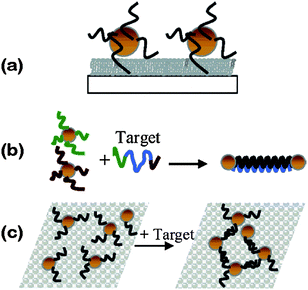
To optimize and extend the sensing applications of NPs, methods must be developed to precisely control the assembly and organization of NPs into various multidimensional, highly ordered arrays.39 In the last decade, numerous approaches were reported for the assembly of NPs into various types of highly ordered superstructures, such as 1D or 2D NP arrays and three-dimensional (3D) superlattices (Fig. 1). The ordered NP assemblies in different dimensions may be constructed either by utilizing the physical interactions among the NPs or by taking advantage of polymer40 and biomolecules41 as binders for the NPs. In self-assembly processes, noncovalent interactions (including electrostatic, hydrogen bonding, and van der Waals interactions),42 specific biorecognition, surface free energy, chemical conjugation or polar interactions have been employed previously to create such controlled assemblies of NPs. These interactions help NPs to generate 1D, 2D and 3D structures and tune the physical response of NPs, which can be further applied in the field of sensors. There are many reviews available, depicting the assembly of NPs in different dimensions with control of their structural aspects and properties.43,44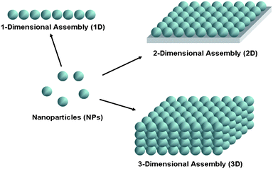 | ||
| Fig. 1 Schematic images of highly ordered 1D, 2D and 3D assemblies of NPs. | ||
3. One-dimensional (1D) assembly of NPs for sensors
The use of NP assemblies as sensors is multifold. In general, they can be classified into either optical or electrical sensors based on the detected signals.3.1. Optical sensors
As described above, 1D chains of NPs can be prepared either by assembly of the pre-formed NPs or with help of linear templates. Readers can refer to several excellent reviews to obtain further information about these studies.45–47 In self-assembed 1D structures of chemically-prepared NPs, both the length and the grafting density of the surface stabilizers determine the minimum inter-NP distance. The organization of both metal and semiconductor NPs in 1D assemblies may have unique optical and electrical properties due to inter-NP electronic, photonic, and energy transfer.48 Several groups have shown that localized surface plasmon resonance (LSPR) coupling between metal NPs in 1D assemblies occurs in the near-field region49 and that electromagnetic energy propagates over a distance of a few hundred nanometres50,51 to create a plasmon-based waveguide.52 Moreover, such long range photonic interactions give rise to giant electromagnetic field enhancements, which make 1D NP assemblies also excellent candidates for surface-enhanced Raman scattering (SERS) active substrates (the details on NP assemblies-based SERS are discussed in Part 4.2).53 For example, citrate-stabilized Ag NPs were linearly assembled into chains by the addition of an appropriate amount of cetyltrimethyl ammonium bromide (CTAB) surfactant,54,55 because CTAB molecules preferentially bonded to the {100} rather than {111} facets56 and thus linked together the {100} facets of neighboring Ag NPs (Fig. 2a). The chain length of 1D Ag arrays could be controlled by adjusting the addition amount of CTAB. The 1D Ag NP assemblies with different lengths were then deposited onto the cationic polyelectrolyte-modified glass substrates. The detected dye molecules, rhodamine 6G (R6G), on the Ag NP chains displayed an increase in the intensity of the SERS spectra with the increasing of chain lengths, which was ascribed to an increasing number of interparticle hot spots (Fig. 2c). The SERS enhancement factor was estimated to be about 2.6 × 10⁸ for R6G, about two orders of magnitude higher than that of isolated Ag NPs.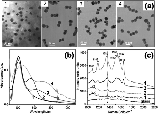 | ||
| Fig. 2 (a) TEM images of 1D Ag NP assemblies: (1) monodisperse Ag colloids, (2) two, (3) three, and (4) four Ag NP chains. (b) Extinction spectra of 1D Ag NP chains corresponding to the samples in (a). (c) SERS spectra of 100 mM R6G adsorbed on glass and 5 nM R6G adsorbed on Ag film prepared by self-assembly on PDDA-modified glass with Ag NP chains 1, 2, 3, and 4 in (a). Reproduced with permission from ref. 55. Copyright 2007, American Chemical Society. | ||
The optical properties of a 1D complex self-assembled structure are also used for sensing. As shown in Fig. 3a, a 1D superstructure of CdTe nanowires (NWs) with mobile excitons and Au NPs with localized plasmons was fabricated. The CdTe NWs and Au NPs were connected by a molecular spring (Fig. 3a), a linear bifunctional poly(ethyleneglycol) (PEG) oligomer (MW = 3400 Da) with N-hydroxy-sulfosuccinimide (NHS) and t-butoxycarbonyl (t-BOC) groups. The molecular spring could reversibly change the distance between the exciton in CdTe NWs and the plasmon on the Au NP surfaces.57 Such 1D NW/NP assemblies were used as biosensors or imaging contrast agents by incorporating antibodies (aB) into the PEG chain as PEG-aB-PEG (Fig. 3b). During the attachment of NPs to the NW, the characteristic surface plasmon peak of Au NPs at 540 nm (Fig. 3b) did not exhibit any spectral shift, except some broadening, which implied that no agglomeration of Au NPs took place and that they remained as individual colloids. However, the photoluminescence (PL) peak of CdTe NWs in the superstructure exhibited a blue-shift of 8–10 nm (1 → 2 in Fig. 3c) due to exciton–plasmon interactions, which were strongly dependent on the NW–NP distance. When streptavidin (SA) was added, the free SA formed an immunocomplex with the anti-streptavidin aB in the PEG chains, which extended the structure of molecular spring. Consequently, the exciton–plasmon interactions decreased, which made the excitons have enough time to diffuse along the NW and to find a site with lower energy, and thus a red-shift of the PL spectra of NW was observed (2 → 3 in Fig. 3c). The processes of the PL wavelength shift in such structures were reversible. Moreover, the PL wavelength was dependent on the concentration of SA (Fig. 3d). The above results demonstrate that the modulation of exciton–plasmon interactions in 1D NP superstructures can serve as a wavelength-based biodetection tool by monitoring the changes in the PL wavelength as a transduction mechanism, which provides a means to resolve problems in the quantification of PL in complex biofluids.
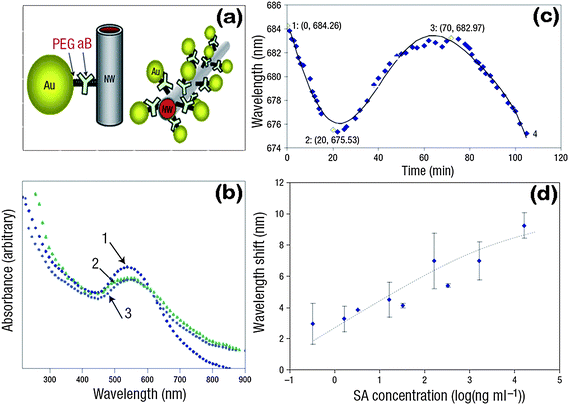 | ||
| Fig. 3 (a) Scheme of 1D Au NP/CdTe NW superstructure. (b) Absorption spectra of Au NPs at each conjugation step: 1, Au NP; 2, after attachment of PEG-aB complexes; 3, after the complete assembly of the MSA in (a). (c) Reversible shift of the peak luminescence wavelength: 1, attachment of a NP to a NW; 2, after adding 20 µL SA; 3, after adding free aB to the media; 4, after adding 20 µL SA. Excitation wavelength: 420 nm. (d) Calibration curve for SA. Reproduced with permission from ref. 57. Copyright 2007, Nature publishing group. | ||
3.2. Electrical sensors
Except for optical properties, the electrical coupling between NPs in 1D assemblies has been used for sensing. For instance, Pd or Pd-based alloys are known to have high sensitivity and selectivity towards hydrogen, and are able to detect hydrogen at near room temperature, so 1D arrays of Pd NPs prepared by an electrochemical reduction method were adopted as rapid and high-performance hydrogen gas sensors.58,59 The ability of hydrogen atoms to occupy the octahedral interstitial positions within Pd's face centered cubic (FCC) lattice structure formed the basis for these sensors. The incorporation of hydrogen atoms generated Pd hydride, leading to the expansion of the crystalline lattice of Pd. As a result, the gap between Pd NPs in 1D assemblies decreased, thus improving the electron transport along the chains (Fig. 4a). On venting the H2 the gaps opened up again. Such reversible responses made 1D Pd NP arrays become high-performance hydrogen gas sensors. The response time of such sensors was less than 75 milliseconds (Fig. 4d), and the decrease of the electrical resistance was correlated with the hydrogen concentration over a range from 2 to 10% (Fig. 4b and 4c). Analogously, other hydrogen sensors were fabricated from 1D hybrid structures of Pd-decorated nanowires and nanotubes.60–65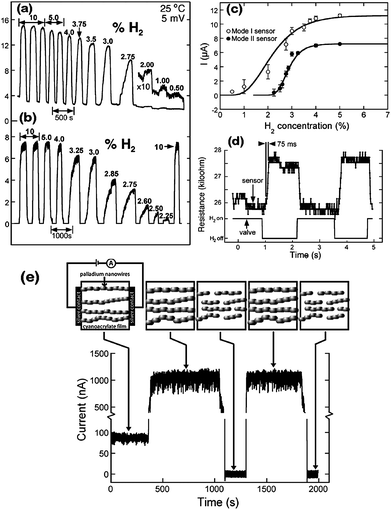 | ||
| Fig. 4 Current response of 1D Pd NP assemblies to hydrogen/nitrogen mixtures (a) and (b). (c) Current amplitude versus H2 concentration for the two sensors of mode I and mode II. (d) Sensor resistance versus time response for a mode I sensor. (e) Electrical response mechanism of 1D Pd NP assemblies. Reproduced with permission from ref. 58. Copyright 2001, AAAS. | ||
4. Two-dimensional (2D) assembly of NPs for sensors
2D assemblies of NPs are a big challenge for scientists, and are mostly prepared using the techniques of solid templates, Langmuir–Blodgett (LB) deposition, or evaporative self-assembly until now.44 Various types of 2D NP assemblies have been investigated for materials and biological applications. Of particular interest in this field is that a 2D assembly of noble metal NPs features optical properties as a function of particle spacing, size, and composition. Therefore, the utilization of 2D metal NP assemblies as optical sensors is highlighted in this part.4.1. Sensors based on localized surface plasmon resonance (LSPR)
The light incident on the metal NPs induces the conduction electrons in them to oscillate collectively with a resonant frequency that depends on the NP’s size, shape, composition, and the inter-NP distance. The DNA detection based on LSPR modes of DNA-capped gold NPs has increased the diagnosis sensitivity by several orders of magnitude since the light scattered from one gold NP is equivalent to the light emitted from over 105 fluorophores.6,66,67 Strong LSPR effect enables noble metal NPs to serve as brightly colored labels for immunoassays,7,68,69 biochemical sensors70–74 and cellular imaging.75–77 Many nascent technologies based on the excellent elastic light-scattering properties of metal NPs73,76,78,79 and also on the shift of the plasmon band maxima with local dielectric constant73,80 have emerged.Another intriguing property of the LSPR effect is the gradual red-shift of the absorption peak position when metal NPs in the assemblies are close each other, which can be described by the Maxwell–Garnett theory. So, 2D or 3D NP assemblies are broadly employed as LSPR sensors, and some reviews have highlighted the recent development in this research topic.81 As shown in Fig. 5a, a 2D monolayer of DNA-modified gold NPs was adsorbed onto a lipid layer supported on a solid substrate through electrostatic interactions.82 Using a lipid layer to support the NPs was due to its 2D fluidity, which allowed the NPs to move along the surface.83 In a typical sensor, there were two sets of gold NPs adsorbed at an equal ratio on the lipid layer, and each set had been previously modified by oligonucleotides of sequences (Fig. 5b). The new sensor was able to recognize a target sequence containing the complementary DNA sequence to both types of probe sequences present. The hybridization between the target and the mobile NP probes was believed to create links between the NPs, resulting in the formation of 2D NP colorimetric (red-shift of absorption) DNA sensors.
 | ||
| Fig. 5 (a) Scheme of the detection device. The system consists of three layers: an organic or inorganic substrate; a lipid layer; and oligonucleotide-modified gold NPs. (b) NPs assembling via DNA hybridization. Two sets of NPs are prepared with different probe oligonucleotides. Addition of a complementary target DNA leads to NP aggregation through hybridization of the target DNA with the probe oligonucleotides. (c) Top view of the system before and after hybridization. Reproduced with permission from ref. 82. Copyright 2006, American Chemical Society. | ||
4.2. Sensors based on surface-enhanced Raman scattering (SERS)
Organic molecules adsorbed to the surface of gold and silver NPs undergo enhanced surface-enhanced Raman scattering (SERS) effects, due to the coupling of the plasmon band of the irradiated metal with the molecules' electronic states.84–86 Although the exact nature of the huge enhancement of Raman intensity found in SERS is still a matter of controversy, the observed enhancement is often attributed to contributions from two mechanisms: (1) a long-range electromagnetic effect wherein the local electromagnetic field at or near laser-irradiated noble metal particle surfaces is enhanced as a result of the localized surface plasmon excitation, leading to more intense Raman scattering from molecules near or adsorbed onto the particle surfaces, and (2) a short-range chemical effect that involves specific interactions or coupling between analyte molecules and the metal particles.85–94 Therefore, two routes are developed to control the optical properties of the substrate to fully maximize SERS intensities, and accordingly lower the analytical limit of detection (LOD) in electromagnetic enhancement mechanisms and chemical enhancement mechanisms.95 The former is responsible for the major portion of SERS enhancement, while the characteristics of metal nanostructures largely affect the magnitude of the electric field.The key to the practical use of SERS-based sensors is creating well-defined, defect-free ordered and reproducible SERS substrates with large and stable Raman enhancement. 2D periodic arrays of metal NPs has two advantages over disordered arrays: the specific surface density of hot spots can be maximized when the NPs are organized in a close-packed manner with the long-range effect providing additional Raman enhancement, and the enhancement factors of 2D periodic arrays can be several orders of magnitude higher than those of disordered metal NP films due to the reduced losses (retardation or damping effects). Theoretical calculations reveal a dramatic narrowing of the extinction peak caused by coherent interactions between particles in a periodic 1D or 2D array,96 and the narrow peaks result from mixing between the localized plasmon resonance of each particle and photonic modes of the particle array. A minimum particle size of 30 nm and a minimum array size of 50 particles are required to produce strong enough coupling to give narrow lines. Similarly, theoretical studies have indicated that electromagnetic field and surface-averaged signal enhancement factors, resonant Gav values from optimized 2D arrays, can be several orders of magnitude greater than those produced by disordered metal aggregates.97,98
Experiments with two-dimensional arrays of metal NPs have confirmed theoretical calculations.99 Atomic force microscopy directly observed the hot spots formed at the junction of two NP aggregates, which played a major role in single molecule SERS (SMSERS).100,101 Many 2D periodic assembled nanostructures fabricated by different procedures, such as self-assembly, LB,13,102,103 nanosphere lithography104,105 and templating, have been used as the substrates for actual SERS measurement.106 The reader is referred to detailed reviews.95 Among those, the substrates of 2D NP assemblies have two great advantages over conventional lithographic methods: the preparation of extremely narrow inter-NP gaps (several nanometres) enables large electromagnetic-field enhancement, and the close-packed structures provide a maximum surface density of hot spots within an illuminated area. For example, large-area hexagonal close-packed structures of alkanethiol-stabilized Ag NPs were prepared by drop evaporation onto a solid substrate, and the inter-NP spacings were finely tuned by controlling the alkyl chain lengths of alkanethiols.107 Such 2D Ag NP arrays possessed a SERS enhancement factor of 105 for R6G.108 The optimum size of metal NPs for maximum SERS enhancement is found to be within 30–80 nm,109 however, the periodic assembly of such larger metal NPs is a challenging task. Both the attractive capillary forces and van der Waals attractions increase with increasing NP size, and especially the capillary forces are quadratic to the NP sizes, which may exceed 100 KT for NPs with sizes 30–80 nm110,111 Such large inter-NP interactions prevent the formation of perfect periodic 2D metal NP arrays.112 This problem can be solved by the use of suitable surfactants. A calixarene-based surfactant containing several hydrocarbon tails was employed to provide strong repulsive forces and thus enhance the dispersion and self-assembly of gold NPs with large diameters into a highly ordered, close-packed 2D structure (Fig. 6a).113,114 Interestingly, the inter-NP spacing decreased from 1 to 0.4 nm with the increase in NP diameter due to the increased van der Waals attraction. The prepared 2D NP arrays exhibited size-dependent SERS activities. The SERS signal intensities were dependent on both excitation wavelength and array periodicity, which were correlated with the size-dependent changes in plasmon resonance, with signal intensities varying by two orders of magnitude under identical sampling conditions and surface coverage (Fig. 6b). Moreover, surfactant CTAB was also used for the assembly of large Au NPs (50 nm diameter)115 or Au nanoshells116 into 2D periodic arrays. The inter-NP spacing on the resulting 2D Au NP arrays was about 8 nm, which possessed a SERS enhancement factor of 108 for para-mercaptoaniline (pMA) molecules.
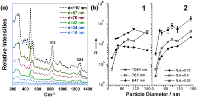 | ||
| Fig. 6 (a) SERS spectra of resorcinarene 6 from Au NP arrays, using an excitation wavelength of 785 nm (10 mW, area = 700 µm2, exposure = 30 s).112 (b) SERS enhancement factors (G) as a function of NP array structures, based on the integrated signal at 813 cm−1 from resorcinarene 6.114 (1) G values at excitation wavelengths of 647, 785 and 1064 nm; (2) G values obtained at 785 nm using different solid angles, as determined by the numerical aperture (N.A.) of the collection objective. Reproduced with permission from ref. 112 and 114. Copyright 2001, John Wiley & Sons, Inc. | ||
Except for the giant electromagnetic enhancement effect of the substrate, most SERS experiments have demonstrated that the analytes need to be chemisorbed to the metal surface for electron transfer occurring, which is called the chemical enhancement effect. These features make SERS particularly useful for the detection of the most abundant, highly Raman active species or the species with the highest affinity for gold or silver NPs. Thus, functionalizing the 2D array of metal NPs with antibodies or DNA targets can turn them into highly molecularly specific optical probes, and can achieve the additional 3 orders of enhancements by charge-transfer and resonance Raman effects.86 In last decade, many groups have used this approach to successfully detect different anions,117–123Bacillus subtilis spores,124 to identify cancer genes and viral DNA,125–127 even to in vivo detect individual cells such as cancer cells in live animals with extremely high sensitivity.128 As an example, the prostate-specific antigen (PSA), a well-established biomarker for the prostate cancer, was analyzed after binding with the nanoconjugates of a specific antibody and bifunctional gold NPs, which were pre-modified with a monolayer of Raman-active molecules. Very low PSA concentration (several pg mL−1) in serum was detected.129 Furthermore, 2D periodic silver nanostructures produced by nanosphere lithography was used for the rapid detection of the extracted calciumdipicolinate (CaDPA) from Bacillus subtilis spores, which was a spore biomarker for anthrax. The detection limit was found to be 2.1 × 10⁻¹⁴ M for Bacillus subtilis spores, i.e. ≈ 2550 anthrax spores, with a data acquisition period of 1 min.130 Such 2D periodic metallic nanostructures fabricated by nanosphere lithography had highly tunable LSPR, however, the chemical stability was limited due to the oxidation of the silver. A Raman interface to scanning electron microscopy (SEM) was also developed for bacterial analysis and has demonstrated the identification of SERS-active regions in the matrix through SEM imaging.131
It should be stressed that, besides spherical NPs, 2D assemblies of NPs with other shapes can also be employed for SERS sensors. As shown in Fig. 7, a 2D monolayer of thiol-capped Ag nanowires was used as a SERS substrate for the ultrasensitive detection of explosives, 2,4-dinitrotoluene (2,4-DNT).13 The -NO2 stretching mode at 1348 cm−1 is clearly displayed and well-separated from the surfactant-related Raman bands at 1295 and 1435 cm−1. The sensitivity is approximately 0.7 pg.
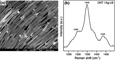 | ||
| Fig. 7 (a) Scanning electron microscopy images of the silver nanowire monolayer deposited on a silicon wafer. (b) SERS spectrum of 2,4-DNT on the thiol-capped Ag nanowire monolayer. Reproduced with permission from ref. 13. Copyright 2003, American Chemical Society. | ||
4.3. Sensors based on surface-enhanced fluorescence (SEF)
Fluorescence detection presently is a central technology in the biosciences. Fluorescence can be enhanced by 1–3 orders of magnitude when a fluorophore is within 3–50 nm from the surface of the metallic nanostructures accompanied by a reduction in the fluorescence lifetime.132–139 This phenomenon is called surface-enhanced fluorescence (SEF), and also called metal-enhanced fluorescence (MEF). SEF bears some analogies to SERS except for the difference in distance dependence. In the case of SEF, an enhanced fluorescence signal occurs when the molecule is ∼10–100 nm away from the metal surface, whereas for SERS the spectral signal of a molecule is intensified by adsorbed or close to the metal NPs. The phenomenon of fluorescence enhancement and decreased fluorescence lifetime is theoretically explained by modified radiative and nonradiative decay rates of fluorophores interacting with surface plasmons, which are dependent on the distance between fluorophore and metal surface, transition moment orientation, wavelength, and quantum yield. The fluorescence of both organic dyes and inorganic semiconductor quantum dots (QDs) is observed to be enhanced by metal NPs.140–144 Among different types of metal NPs, silver nanostructures are the most used. SEF with silver island films (SIF) and 2D monolayers of silver NPs have been extensively used in fluorescence assays or single molecule detection for biological functionalities, for example, DNA,145–148 cell imaging,149 protein–protein and protein–small molecule interactions.140 One disadvantage of SEF sensors is that fluorescence enhancement and reduction of photobleaching on rough metallic surfaces are usually accompanied by a loss of optical resolution due to refraction of light by particles, which can be partially improved by using 2D silver NP assemblies, rather than silver island films, as the substrates because Ag NPs are made with well-defined sizes and low heterogeneity. As shown in Fig. 8d and 8e, the resolution of the optical images of phalloidin-labeled muscle myofibrils on 2D NP assemblies was as good as on glass, as evidenced by the fact that both H-zones (arrows) and Z-lines (arrowhead) were seen.150 Meanwhile, the fluorescence intensity of the myofibrils on small and large Ag NP-coated substrates was, respectively, 18 and 33 times higher than that on plain glass substrates (Fig. 8f).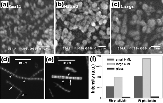 | ||
| Fig. 8 Scanning electron microscopy images of Ag NPs with median diameters of 60, 50, and 70 nm, respectively, for small- (a), mixed- (b), and large-sized (c) NPs. Image of myofibrils on glass coverslip (d) and 2D Ag NP assemblies (e). (f) Fluorescence intensities of myofibrils labeled with rhodamine–phalloidin (left) and fluorescein–phalloidin (right). Myofibrils were on glass (black) coverslip or on glass coated with 2D assemblies containing large (light gray) and small (dark gray) NPs. Reproduced with permission from ref. 150. Copyright 2008, Elsevier. | ||
5. Three-dimensional (3D) assembly of NPs for sensing
3D assembly of NPs can be achieved in the form of layered nanostructures, as an extension of another dimension to the 2D pathway, using multiple-sheet assembly, or 3D templates. The approaches include evaporation-induced assembly, Langmuir–Blodgett technique, layer-by-layer assembly (LbL), and scanning probe microscopy (SPM) manipulation. There has been a long history of applying 3D NP assemblies in sensing, and the readers can refer to some excellent reviews to achieve the exclusive information.28,151,152 Herein, we introduce the basic principles of 3D NP assemblies as sensors, and highlight the recent progress in this field.5.1. Optical sensors
3D assemblies of metal and semiconductor NPs are attracting intense attention for sensing applications since they display unique optical properties which are distinct from their respective bulk and individual NP characteristics. Analogously to 2D NP assemblies, dramatic enhancement of the electromagnetic field in 3D metal NP assemblies make themselves good candidates as SERS sensors153–157 and LSPR sensor substrates.158,159 One example is the utilization of 3D nanocanal arrays, which were composed of uniformly aligned vertical cylindrical pores with inner walls decorated with metal NPs, as efficient SERS substrates for trace-level detection of explosive 2,4-dinitrotoluene (DNT) (Fig. 9).160 Porous alumina membranes with vertical, through nanocanals were beneficial for the efficient light interaction because of optical transparency and waveguide properties. Porous alumina membranes were functionalized with positively charged amine groups by modification with poly(diallyldimethylammonium chloride) (PDDA) polyelectrolyte. CTAB-capped gold NPs were passed through the modified porous membranes, resulting in Au NP immobilization (Fig. 9a) and utilization as a SERS substrate. The Raman spectrum of 100 ppb 2,4-DNT solution evaporated on the SERS substrate clearly showed NO2 stretching modes of DNT at 1342 cm−1, distinctive from several PDDA-related Raman peaks such as νC4N at 783 cm−1 and ρCH3 at 1444 cm−1(Fig. 9b). Notably, the SERS intensity of DNT on NP assemblies in 3D porous structures was much stronger than that on 2D Au NP assemblies on silicon substrates with a similar nanoparticle surface density (100 ppb vs. 1000 ppm). The minimum detection limit estimated from the signal-to-noise ratio for this spectrum was as low as 10 fg. The huge Raman enhancement of NP assemblies in 3D porous structures can be ascribed to the optical waveguide effect of vertical pore arrays with the excited evanescent electrical field. The propagating light can be trapped inside the alumina nanowalls with total internal reflection, leading to a higher photon density of states at the alumina-coating interface and thus an increase in Raman scattering by the interaction of the evanescent field with the Au NP assemblies inside the 3D porous structures.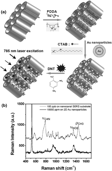 | ||
Fig. 9 (a) Fabrication procedures for nanohole arrays decorated with gold NPs and DNT. (b) Raman spectra of 100 ppb 2,4-DNT drop-evaporated on the SERS substrates with PDDA/Au NPs/PDDA/PAM on top of silicon substrates and control Raman spectra of 10![[thin space (1/6-em)]](https://www.rsc.org/images/entities/char_2009.gif) 000 ppm 2,4-DNT on a 2D substrate. Reproduced with permission from ref. 160. Copyright 2008, John Wiley & Sons, Inc. 000 ppm 2,4-DNT on a 2D substrate. Reproduced with permission from ref. 160. Copyright 2008, John Wiley & Sons, Inc. | ||
Except for metal NPs, the optical properties of 3D semiconductor NP assemblies can be used for detecting chemicals or biomolecules. Very recently, our group161 prepared a blood glucose sensor based on 3D multilayer films of CdTe NPs and glucose oxidase (GOD) by using the layer-by-layer (LBL) assembly technique, which was based on the alternative deposition of opposite-charged species on the substrates42 (Fig. 10a). Previous reports confirmed that the optical, electrical, and electrochemical response of NPs in the multilayer film could be tailored through the layer architecture.162,163 So the LBL self assembly technique might offer an alternative way to develop a new generation of nanocomposite biosensors.164,165 When 3D multilayer films of CdTe NPs and GOD were contacted with glucose solution, the PL of NPs in the films was quickly quenched because the enzyme-catalyzed reaction product (H2O2) of GOD and glucose led to the production of surface defects on the NPs. The quenching rate was a function of the concentration of glucose (as shown in Fig. 10b). The linear range and sensitivity for glucose determination could be adjusted by controlling the layers of NPs and GOD. The biosensor was used to successfully determine the concentration of blood glucose in real serum samples without sample pretreatment and exhibited satisfactory reproducibility and accuracy. Evidently, it will offer new routes for the fabrication and application of sensors by ordered integration of biomolecules with specific recognition and NPs with optical/electrical activity into 3D assemblies.
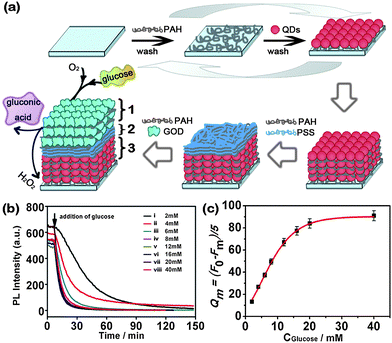 | ||
| Fig. 10 (a) Sensing assembly: (1) top 3 bilayers of PAH/GOD; (2) 3 bilayers of PAH/PSS; (3) 12 bilayers of PAH/CdTe QDs. (b) Time-dependent fluorescence changes recorded at 630 nm upon the interaction of (PAH/CdTe)12(PAH/PSS)3(PAH/GOD)3 multilayer with variable concentrations of glucose: (i) 2; (ii) 4; (iii) 6; (iv) 8; (v) 12; (vi) 16; (vii) 20; (viii) 40 mM. (c) Absolute quenching rate of the PL intensity taken from (a) within 5 min as a function of glucose concentration. F0 and Fm represent the PL intensity of (PAH/CdTe)12(PAH/PSS)3(PAH/GOD)3 multilayer at emission maximum in the absence (F0) and presence (Fm) of glucose. Reproduced with permission from ref. 161. Copyright 2009, American Chemical Society. | ||
5.2. Electrical sensors
The electrical properties of 3D NP assemblies can be tuned by varying the size or shape of the NP components as well as the inter-NP distance, which provides many opportunities for sensor design. For instance, an insulator–metal transition has been observed in 2D and 3D assemblies of metal NPs by changing the interparticle distance.158,166–170 Changes in the charge transport properties of self-assembled metal NP films are accompanied by changes in the optical absorption characteristics. In the insulating regime of 3D networks of metal NPs, an increase in conductivity is accompanied by a broadening and red-shift of the plasmon absorption band, leading to an increase in the absorption in the near-infrared,157,158,168,170,171 which may benefit their applications as biosensors.Alternatively, the unique electrical properties of 3D semiconductor NP assemblies make themselves attractive for the fabrication of photoconductive photodetectors. Different with conventional photodiodes that convey one electron's worth of current per photon incident, photoconductive photodetectors of 3D semiconductor NP assemblies can show considerable gain upon an incident light. As shown in Fig. 11a, the 3D nanocomposite of PbS NPs and the conjugated polymer poly[2-methoxy-5-(2′-ethylhexyloxy-p-phenylenevinylene)] (MEH-PPV) was deposited onto a PPV-coated ITO electrode.172 PbS NPs effectively sensitized MEH-PPV from its own absorbed region between ∼400 nm and ∼600 nm to the near-infrared with sensitivity far beyond 800 nm, resulting in the harvesting of infrared-photogenerated carriers and production of an infrared photovoltaic effect. By varying the size of the NPs, the peaks of the photocurrent spectra could be tailored to 980 nm, 1200 nm and 1355 nm. The resulting device exhibited, at a bias of −5 V and under illumination from a 975 nm laser, a photocurrent of 8.43 µA under 2.7 mW incident power and 90.61 µA under 207 mW incident power. The maximum ratio of photocurrent to dark current was 630, and the maximum responsivity was 3.1 × 10⁻³ A W−1. More interestingly, the photo-responsivity could be further improved by using pure 3D NP assemblies rather than a nanocomposite of MEH-PPV and PbS NPs.173,174 3D n-butylamine-capped PbS NP arrays were deposited by a spin-coating technique onto gold interdigitated electrodes with inter-electrode separation of 5 mm and the metal electrode height of 100 nm (Fig. 11b). The thickness of the NP assemblies formed was 800 nm. Then the device was immersed in methanol to remove butylamine ligands for further decreasing the interparticle separation, causing necking, or crosslinking, at points where adjacent NPs' surfaces were in contact with one another. The devices showed high photoconductive gains with a response greater than 103 A W−1 as a result of long carrier lifetime and high mobility. The best devices exhibited a superior normalized detectivity D* (D*, the figure of merit for detector sensitivity) of 1.8 × 10¹³ Jones (1 Jones = 1 cm Hz1/2 W−1) at 1.3 µm at room temperature. Similarly, other semiconductor NPs, such as Ag2S,175 ZnSe:Mg,176 Bi2S3,177 ZnO,178 Cu2S combined with CdS,179 PbSe,180 and Bi2S3181 have also been employed as candidates for photodetectors.
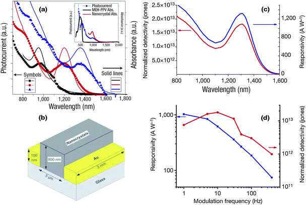 | ||
| Fig. 11 (a) Photocurrent spectral responses and absorption spectra. Main panel: photocurrent spectral response (symbols) and the corresponding absorption spectra (solid line) for three different samples.172 The absorption peaks are tuned to 955 (black), 1200 (red) and 1355 nm (blue). (b) Device structure of 3D PbS NP assemblies.173 (c) Spectra of responsivity and normalized detectivity D* of neck-then-oxidize NP devices.173 (d) Electrical frequency response of the same devices under 40 V bias.173 Reproduced with permission from ref. 172 and 173. Copyright 2006, Nature publishing group. | ||
The 3D assembly of NPs crosslinked with an organic matrix is another intriguing feature for various sensor applications. The electrical coupling between adjacent NPs is controlled by the dielectric nature of the embedding organic matrix, and thus, if chemical functionality is introduced into the organic matrix, the high sensitivity of the electrical properties of such assemblies toward their composition will open possibilities for a chemiresistor-type sensing application.182–190 As an example, 3D octanethiol-stabilized Au NP assemblies were demonstrated to respond with a fast, reversible, and very sensitive increase of their resistance when exposed to vapors of toluene or tetrachloroethylene, due to the expanded configuration of an octanethiol matrix in organic vapor.184 A bis-bipyridinium cyclophane-crosslinked 3D array of Au NPs provided an effective assembly for the electrochemical sensing of π-donor substrates, e.g. p-hydroquinone or adrenaline.191 3D Au NP assemblies crosslinked by microperoxidase-11 on transparent ITO electrodes exhibited a tunable electrocatalytic activity for the reduction of H2O2, and the sensitivity of the H2O2-sensing interface could be tuned by controlling the number of Au NPs in the assemblies.192
6. Concluding remarks and prospects
Thanks to recent progress of NP synthesis and assembly techniques, NP assemblies with different dimensions start to be extensively employed in chemical and biological sensing, and have shown numerous advantages over conventional sensors, for example, high sensitivity, low detect limits, super selectivity, fast responses, and small sizes. Because utilization of NP assemblies as sensors is still in the burgeoning stage, a lot of opportunities await to be explored.Firstly, novel designs of NP assemblies are highly desirable. Until now, most researchers mainly focused on the fabrication of simple 1D, 2D and 3D NP assemblies, and certainly NP assemblies with hierarchical structures will dramatically extend their applications in sensors. As an example, very recently chiral NP assemblies were successfully prepared,193 and such assemblies may open applications in recognition of chiral biomolecules or chemicals.194,195
Secondly, deep understanding of the collective properties of NP assemblies will help us to find new applications in sensors. For instance, 2D metal NP assemblies are used to improve the resolution of IR spectra of organic molecules due to strong coupling between surface plasmon resonance of metal NPs and absorption characteristics of organic molecules in the IR region.116 Because the IR technique has been extensively used to identify organic and biomolecules, such enhancement effects of NP assemblies can be anticipated to have an important application.
Thirdly, more work will be put into the study of reproducibility and robustness of NP assemblies based on the consideration of practical applications. One big concern is the possible structure and property change of NP assemblies during detections due to the meta-stable nature of NPs in assemblies. Some general strategies should be developed to improve the stability of NP assemblies without the loss of their unique electrical/optical properties.
In summary, the NP assembly sensors have shown a bright promise in the field of both chemical and biological detections, and we can expect a fast development of the corresponding research in the near future.
Acknowledgements
This work was supported by National High-tech Research and Development Program (2007AA03Z302, ZYT, SQL), 100-talent program of Chinese Academy of Sciences (ZYT), Start-up funding of HIT (SQL), the National Science Foundation of China (20773033, ZYT), and the National Research Fund for Fundamental Key Project (2009CB930401, ZYT).References
- A. P. Alivisatos, Science, 1996, 271, 933–937 CrossRef CAS.
- C. B. Murray, C. R. Kagan and M. G. Bawendi, Annu. Rev. Mater. Sci., 2000, 30, 545–610 CrossRef CAS.
- M. Grzelczak, J. Pérez-Juste, P. Mulvaney and L. M. Liz-Marzán, Chem. Soc. Rev., 2008, 37, 1783–1791 RSC.
- G. L. Hornyak, C. J. Patrissi and C. R. Martin, J. Phys. Chem. B, 1997, 101, 1548–1555 CrossRef CAS.
- S. Link and M. A. El-Sayed, J. Phys. Chem. B, 1999, 103, 8410–8426 CrossRef CAS.
- R. Elghanian, J. J. Storhoff, R. C. Mucic, R. L. Letsinger and C. A. Mirkin, Science, 1997, 277, 1078–1081 CrossRef CAS.
- S. Schultz, D. R. Smith, J. J. Mock and D. A. Schultz, Proc. Natl. Acad. Sci. U. S. A., 2000, 97, 996–1001 CrossRef CAS.
- J. J. Mock, M. Barbic, D. R. Smith, D. A. Schultz and S. Schultz, J. Chem. Phys., 2002, 116, 6755–6759 CrossRef CAS.
- J. P. Kottmann, O. J. F. Martin, D. R. Smith and S. Schultz, Chem. Phys. Lett., 2001, 341, 1–6 CrossRef CAS.
- K. L. Kelly, E. Coronado, L. L. Zhao and G. C. Schatz, J. Phys. Chem. B, 2003, 107, 668–677 CrossRef CAS.
- I. O. Sosa, C. Noguez and R. G. Barrera, J. Phys. Chem. B, 2003, 107, 6269–6275 CrossRef CAS.
- K. Imura, T. Nagahara and H. Okamoto, J. Am. Chem. Soc., 2004, 126, 12730–12731 CAS.
- A. Tao, F. Kim, C. Hess, J. Goldberger, R. He, Y. Sun, Y. Xia and P. Yang, Nano Lett., 2003, 3, 1229–1233 CrossRef CAS.
- P. Hanarp, M. Kall and D. S. Sutherland, J. Phys. Chem. B, 2003, 107, 5768–5772 CrossRef CAS.
- M. Gluodenis and C. A. Foss, J. Phys. Chem. B, 2002, 106, 9484–9489 CrossRef CAS.
- B. Nikoobakht and M. A. El-Sayed, J. Phys. Chem. A, 2003, 107, 3372–3378 CrossRef CAS.
- U. Kreibig and M. Vollemer, Optical Properties of Metal Cluster, Springer, Berlin, 1995 Search PubMed.
- P. Mulvaney, Langmuir, 1996, 12, 788–800 CrossRef CAS.
- H. Bönnemann and R. M. Richards, Eur. J. Inorg. Chem., 2001, 2455–2480 CrossRef CAS.
- C. M. Niemeyer, Angew. Chem., Int. Ed., 2001, 40, 4128–4158 CrossRef CAS.
- U. Simon, in Nanoparticles From Theory to Application, ed. G. Schmid, Wiley-VCH, Weinheim, 2004, pp. 328–367 Search PubMed.
- B. Yu and M. Meyyappan, Solid-State Electron., 2006, 50, 536–544 CrossRef CAS.
- A. N. Shipway, E. Katz and I. Willner, ChemPhysChem, 2000, 1, 18–52 CrossRef CAS.
- M. A. El-Sayed, Acc. Chem. Res., 2001, 34, 257–264 CrossRef CAS.
- D. L. Feldheim and C. A. Foss, Metal Nanoparticles: Synthesis, Characterization and Applications, Marcel Dekker, New York, 2002 Search PubMed.
- M.-C. Daniel and D. Astruc, Chem. Rev., 2004, 104, 293–346 CrossRef CAS.
- S. Sun, S. Anders, T. Thomson, J. E. E. Baglin, M. F. Toney, H. F. Hamann, C. B. Murray and B. D. Terris, J. Phys. Chem. B, 2003, 107, 5419–5425 CrossRef CAS.
- N. L. Rosi and C. A. Mirkin, Chem. Rev., 2005, 105, 1547–1562 CrossRef CAS.
- A. Wieckowski, E. R. Savinova and C. G. Vayenas, Catalysis and electrocatalysis at nanoparticle surfaces, Marcel Dekker, New York, 2003 Search PubMed.
- J. J. Urban, D. V. Talapin, E. V. Shevchenko and C. B. Murray, J. Am. Chem. Soc., 2006, 128, 3248–3255 CrossRef CAS.
- M. Giersig and M. Hilgendorff, Eur. J. Inorg. Chem., 2005, 3571–3583 CrossRef CAS.
- M. P. Pileni, J. Phys. Chem. B, 2001, 105, 3358–3371 CrossRef CAS.
- M. P. Pileni, Y. Lalatonne, D. Ingert, I. Lisiecki and A. Courty, Faraday Discuss., 2004, 125, 251–264 RSC.
- G. C. Papavassiliou, Prog. Solid State Chem., 1979, 12, 185–271 CrossRef CAS.
- R. Gans, Ann. Phys., 1915, 352, 270 CrossRef.
- M. B. Mohamed, K. Z. Ismail, S. Link and M. A. El-Sayed, J. Phys. Chem. B, 1998, 102, 9370–9374 CrossRef CAS.
- E. M. Hicks, S. Zou, G. C. Schatz, K. G. Spears, R. P. Van Duyne, L. Gunnarsson, T. Rindzevicius, B. Kasemo and M. Käll, Nano Lett., 2005, 5, 1065–1070 CrossRef CAS.
- A. Taleb, C. Petit and M. P. Pileni, J. Phys. Chem. B, 1998, 102, 2214–2220 CrossRef CAS.
- C. P. Collier, T. Vossmeyer and J. R. Heath, Annu. Rev. Phys. Chem., 1998, 49, 371–404 CrossRef CAS.
- N. A. Kotov, I. Dekany and J. H. Fendler, J. Phys. Chem., 1995, 99, 13065–13069 CrossRef CAS.
- W. E. Ford, O. Harnack, A. Yasuda and J. M. Wessels, Adv. Mater., 2001, 13, 1793–1797 CrossRef CAS.
- G. Decher, Science, 1997, 277, 1232–1237 CrossRef CAS.
- S. Kinge, M. Crego-Calama and D. N. Reinhoudt, ChemPhysChem, 2008, 9, 20–42 CrossRef CAS.
- S. Srivastava and N. A. Kotov, Soft Matter, 2009, 5, 1146–1156 RSC.
- N. R. Jana, L. Gearheart and C. J. Murphy, J. Phys. Chem. B, 2001, 105, 4065–4067 CrossRef CAS.
- L. Gou and C. J. Murphy, Chem. Mater., 2005, 17, 3668–3672 CrossRef CAS.
- Z. Tang and N. A. Kotov, Adv. Mater., 2005, 17, 951–962 CrossRef CAS.
- Z. Tang, B. Ozturk, Y. Wang and N. A. Kotov, J. Phys. Chem. B, 2004, 108, 6927–6931 CrossRef CAS.
- M. Salerno, J. R. Krenn, A. Hohenau, H. Ditlbacher, G. Schider, A. Leitner and F. R. Aussenegg, Opt. Commun., 2005, 248, 543–549 CrossRef CAS.
- S. A. Maier, P. G. Kik and H. A. Atwater, Appl. Phys. Lett., 2002, 81, 1714–1716 CrossRef CAS.
- R. de Waele, A. F. Koenderink and A. Polman, Nano Lett., 2007, 7, 2004–2008 CrossRef CAS.
- S. A. Maier, P. G. Kik, H. A. Atwater, S. Meltzer, E. Harel, B. E. Koel and A. A. G. Requicha, Nat. Mater., 2003, 2, 229–232 CrossRef CAS.
- K. Li, M. I. Stockman and D. J. Bergman, Phys. Rev. Lett., 2003, 91, 227402–227405 CrossRef.
- Y. Yang, S. Matsubara, M. Nogami, J. Shi and W. Huang, Nanotechnology, 2006, 17, 2821–2827 CrossRef CAS.
- Y. Yang, J. Shi, T. Tanaka and M. Nogami, Langmuir, 2007, 23, 12042–12047 CrossRef CAS.
- B. Nikoobakht, Z. L. Wang and M. A. El-Sayed, J. Phys. Chem. B, 2000, 104, 8635–8640 CrossRef CAS.
- J. Lee, P. Hernandez, J. Lee, A. O. Govorov and N. A. Kotov, Nat. Mater., 2007, 6, 291–295 CrossRef CAS.
- F. Favier, E. C. Walter, M. P. Zach, T. Benter and R. M. Penner, Science, 2001, 293, 2227–2231 CrossRef CAS.
- Y. Im, C. Lee, R. P. Vasquez, M. A. Bangar, N. V. Myung, E. J. Menke, R. M. Penner and M. Yun, Small, 2006, 2, 356–358 CrossRef CAS.
- Z. H. Chen, J. S. Jie, L. B. Luo, H. Wang, C. S. Lee and S. T. Lee, Nanotechnology, 2007, 18, 345502 CrossRef.
- H. T. Wang, B. S. Kang, F. Ren, L. C. Tien, P. W. Sadik, D. P. Norton, S. J. Pearton and J. Lin, Appl. Phys. Lett., 2005, 86, 243503 CrossRef.
- J. Kong, M. G. Chapline and H. Dai, Adv. Mater., 2001, 13, 1384–1386 CrossRef CAS.
- S. Mubeen, T. Zhang, B. Yoo, M. A. Deshusses and N. V. Myung, J. Phys. Chem. C, 2007, 111, 6321–6327 CrossRef CAS.
- K. Yao, W. W. Gong, Y. F. Hu, X. L. Liang, Q. Chen and L.-M. Peng, J. Phys. Chem. C, 2008, 112, 8721–8724 CrossRef CAS.
- O. K. Varghese, D. Gong, M. Paulose, K. G. Ong and C. A. Grimes, Sens. Actuators, B, 2003, 93, 338–344 CrossRef.
- C. A. Mirkin, R. L. Letsinger, R. C. Mucic and J. J. Storhoff, Nature, 1996, 382, 607–609 CrossRef CAS.
- T. A. Taton, C. A. Mirkin and R. L. Letsinger, Science, 2000, 289, 1757–1760 CrossRef CAS.
- J. Yguerabide and E. E. Yguerabide, Anal. Biochem., 1998, 262, 137–156 CrossRef CAS.
- J.-M. Nam, C. S. Thaxton and C. A. Mirkin, Science, 2003, 301, 1884–1886 CrossRef CAS.
- C. R. Yonzon, D. A. Stuart, X. Zhang, A. D. McFarland, C. L. Haynes and R. P. V. Duyne, Talanta, 2005, 67, 438–448 CrossRef.
- A. J. Haes, L. Chang, W. L. Klein and R. P. Van Duyne, J. Am. Chem. Soc., 2005, 127, 2264–2271 CrossRef CAS.
- A. B. Dahlin, J. O. Tegenfeldt and F. Hook, Anal. Chem., 2006, 78, 4416–4423 CrossRef CAS.
- A. D. McFarland and R. P. Van Duyne, Nano Lett., 2003, 3, 1057–1062 CrossRef CAS.
- G. Raschke, S. Kowarik, T. Franzl, C. Sonnichsen, T. A. Klar, J. Feldmann, A. Nichtl and K. Kurzinger, Nano Lett., 2003, 3, 935–938 CrossRef CAS.
- K. J. Lee, P. D. Nallathamby, L. M. Browning, C. J. Osgood and X.-H. N. Xu, ACS Nano, 2007, 1, 133–143 CrossRef CAS.
- X.-H. N. Xu, W. J. Brownlow, S. V. Kyriacou, Q. Wan and J. J. Viola, Biochemistry, 2004, 43, 10400–10413 CrossRef CAS.
- C. Loo, A. Lin, L. Hirsch, M.-H. Lee, J. Barton, N. Halas, J. West and R. Drezek, Technol. Cancer Res. Treat., 2004, 3, 33–40 Search PubMed.
- D. A. Schultz, Curr. Opin. Biotechnol., 2003, 14, 13–22 CrossRef CAS.
- X.-H. N. Xu, J. Chen, R. B. Jeffers and S. Kyriacou, Nano Lett., 2002, 2, 175–182 CrossRef CAS.
- A. C. Templeton, J. J. Pietron, R. W. Murray and P. Mulvaney, J. Phys. Chem. B, 2000, 104, 564–570 CrossRef CAS.
- J. N. Anker, W. P. Hall, O. Lyandres, N. C. Shah, J. Zhao and R. P. Van Duyne, Nat. Mater., 2008, 7, 442–453 CrossRef CAS.
- A. Charrier, N. Candoni and F. Thibaudau, J. Phys. Chem. B, 2006, 110, 12896–12900 CrossRef CAS.
- R. C. MacDonald, G. W. Ashley, M. M. Shida, V. A. Rakhmanova, Y. S. Tarahovsky, D. P. Pantazatos, M. T. Kennedy, E. V. Pozharski, K. A. Baker, R. D. Jones, H. S. Rosenzweig, K. L. Choi, R. Qiu and T. J. McIntosh, Biophys. J., 1999, 77, 2612–2629 CrossRef CAS.
- R. L. Garrell, Anal. Chem., 1989, 61, 401A–411A CAS.
- A. Campion and P. Kambhampati, Chem. Soc. Rev., 1998, 27, 241–250 RSC.
- K. Kneipp, H. Kneipp, I. Itzkan, R. R. Dasari and M. S. Feld, Chem. Rev., 1999, 99, 2957–2976 CrossRef CAS.
- A. Otto, in Light Scattering in Solids, ed. G. Güntherodt, M. Cardonaand R. Zeyher, Springer, Berlin/Heidelberg, 1984, pp. 289–418 Search PubMed.
- M. Moskovits, Rev. Mod. Phys., 1985, 57, 783–826 CrossRef CAS.
- M. Moskovits, Top. Appl. Phys., 2006, 103, 1–17 CAS.
- K. Kneipp and H. Kneipp, Isr. J. Chem, 2006, 46, 299–305 CAS.
- J. A. Sánchez-Gil and J. V. García-Ramos, Chem. Phys. Lett., 2003, 367, 361–366 CrossRef CAS.
- J. A. Sánchez-Gil, J. V. García-Ramos and E. R. Méndez, Phys. Rev. B: Condens. Matter Mater. Phys., 2000, 62, 10515–10525 CrossRef CAS.
- M. Sackmann and A. Materny, J. Raman Spectrosc., 2006, 37, 305–310 CrossRef CAS.
- L. Jensen, C. M. Aikens and G. C. Schatz, Chem. Soc. Rev., 2008, 37, 1061–1073 RSC.
- H. Ko, S. Singamaneni and V. V. Tsukruk, Small, 2008, 4, 1576–1599 CrossRef CAS.
- S. Zou, N. Janel and G. C. Schatz, J. Chem. Phys., 2004, 120, 10871–10875 CrossRef CAS.
- S. Zou and G. C. Schatz, Chem. Phys. Lett., 2005, 403, 62–67 CrossRef.
- D. A. Genov, A. K. Sarychev, V. M. Shalaev and A. Wei, Nano Lett., 2004, 4, 153–158 CrossRef CAS.
- C. L. Haynes, A. D. McFarland, L. Zhao, R. P. Van Duyne, G. C. Schatz, L. Gunnarsson, J. Prikulis, B. Kasemo and M. Kall, J. Phys. Chem. B, 2003, 107, 7337–7342 CrossRef CAS.
- A. M. Michaels, M. Nirmal and L. E. Brus, J. Am. Chem. Soc., 1999, 121, 9932–9939 CrossRef CAS.
- A. M. Michaels, Jiang and L. Brus, J. Phys. Chem. B, 2000, 104, 11965–11971 CrossRef CAS.
- Y. Lu, G. L. Liu and L. P. Lee, Nano Lett., 2005, 5, 5–9 CrossRef CAS.
- A. Tao, P. Sinsermsuksakul and P. Yang, Nat. Nanotechnol., 2007, 2, 435–440 Search PubMed.
- J. C. Hulteen and R. P. V. Duyne, J. Vac. Sci. Technol., A, 1995, 13, 1553–1558 CrossRef CAS.
- J. C. Hulteen, D. A. Treichel, M. T. Smith, M. L. Duval, T. R. Jensen and R. P. Van Duyne, J. Phys. Chem. B, 1999, 103, 3854–3863 CrossRef CAS.
- O. D. Velev and A. M. Lenhoff, Curr. Opin. Colloid Interface Sci., 2000, 5, 56–63 CrossRef CAS.
- C.-F. Chen, S.-D. Tzeng, H.-Y. Chen, K.-J. Lin and S. Gwo, J. Am. Chem. Soc., 2008, 130, 824–826 CrossRef CAS.
- T. Qiu, X. L. Wu, J. C. Shen and P. K. Chu, Appl. Phys. Lett., 2006, 89, 131914 CrossRef.
- N. R. Jana and T. Pal, Adv. Mater., 2007, 19, 1761–1765 CrossRef CAS.
- P. A. Kralchevsky and N. D. Denkov, Curr. Opin. Colloid Interface Sci., 2001, 6, 383–401 CrossRef CAS.
- P. A. Kralchevsky, K. D. Danov and N. D. Denkov, in Handbook of Surface and Colloid Chemistry, ed. K. S. Birdi, CRC Press, New York, 2002, ch. 5 Search PubMed.
- A. Wei, Chem. Commun., 2006, 1581–1591 RSC.
- B. Kim, S. L. Tripp and A. Wei, MRS Symp. Proc., 2001, 676 Search PubMed Y.6.1.
- A. Wei, B. Kim, B. Sadtler and S. L. Tripp, ChemPhysChem, 2001, 2, 743–745 CrossRef CAS.
- H. Wang, C. S. Levin and N. J. Halas, J. Am. Chem. Soc., 2005, 127, 14992–14993 CrossRef CAS.
- H. Wang, J. Kundu and Naomi J. Halas, Angew. Chem., Int. Ed., 2007, 46, 9040–9044 CrossRef CAS.
- K.-h. Yea, S. Lee, J. B. Kyong, J. Choo, E. K. Lee, S.-W. Joo and S. Lee, Analyst, 2005, 130, 1009–1011 RSC.
- W. Wang, C. Ruan and B. Gu, Anal. Chim. Acta, 2006, 567, 121–126 CrossRef CAS.
- C. Ruan, W. Wang and B. Gu, Anal. Chim. Acta, 2006, 567, 114–120 CrossRef CAS.
- P. A. Mosier-Boss and S. H. Lieberman, Appl. Spectrosc., 2003, 57, 1129–1137 CrossRef CAS.
- P. A. Mosier-Boss and S. H. Lieberman, Appl. Spectrosc., 2000, 54, 1126–1135 CrossRef CAS.
- S. Tan, M. Erol, A. Attygalle, H. Du and S. Sukhishvili, Langmuir, 2007, 23, 9836–9843 CrossRef CAS.
- S. Tan, M. Erol, S. Sukhishvili and H. Du, Langmuir, 2008, 24, 4765–4771 CrossRef CAS.
- D. A. Stuart, C. R. Yonzon, X. Zhang, O. Lyandres, N. C. Shah, M. R. Glucksberg, J. T. Walsh and R. P. Van Duyne, Anal. Chem., 2005, 77, 4013–4019 CrossRef CAS.
- T. Vo-Dinh, L. R. Allain and D. L. Stokes, J. Raman Spectrosc., 2002, 33, 511–516 CrossRef CAS.
- L. R. Allain and T. Vo-Dinh, Anal. Chim. Acta, 2002, 469, 149–154 CrossRef CAS.
- Y. C. Cao, R. Jin and C. A. Mirkin, Science, 2002, 297, 1536–1540 CrossRef CAS.
- X. M. Qian, X. H. Peng, D. O. Ansari, Q. Yin-Goen, G. Z. Chen, D. M. Shin, L. Yang, A. N. Young, M. D. Wang and S. M. Nie, Nat. Biotechnol., 2008, 26, 83–90 CrossRef CAS.
- D. S. Grubisha, R. J. Lipert, H.-Y. Park, J. Driskell and M. D. Porter, Anal. Chem., 2003, 75, 5936–5943 CrossRef CAS.
- X. Zhang, M. A. Young, O. Lyandres and R. P. Van Duyne, J. Am. Chem. Soc., 2005, 127, 4484–4489 CrossRef CAS.
- R. M. Jarvis, A. Brooker and R. Goodacre, Anal. Chem., 2004, 76, 5198–5202 CrossRef CAS.
- D. A. Weitz, S. Garoff, J. I. Gersten and A. Nitzan, J. Chem. Phys., 1983, 78, 5324–5338 CrossRef CAS.
- J. Kümmerlen, A. Leitner, H. Brunner, F. R. Aussenegg and A. Wokaun, Mol. Phys., 1993, 80, 1031–1046.
- K. Sokolov, G. Chumanov and T. Cotton, Anal. Chem., 1998, 70, 3898–3905 CrossRef CAS.
- J. R. Lakowicz, Y. Shen, S. Dauria, J. Malicka, J. Fang, Z. Gryczynski and I. Gryczynski, Anal. Biochem., 2002, 301, 261–277 CrossRef CAS.
- B. P. Maliwal, J. Malicka, Z. Gryczynski, I. Gryczynski and J. R. Lakowicz, Biopolymers, 2003, 70, 585–594 CrossRef CAS.
- J. Malicka, I. Gryczynski, Z. Gryczynski and J. R. Lakowicz, Anal. Biochem., 2003, 315, 57–66 CrossRef CAS.
- E. G. Matveeva, I. Gryczynski, A. Barnett, Z. Leonenko, J. R. Lakowicz and Z. Gryczynski, Anal. Biochem., 2007, 363, 239–245 CrossRef CAS.
- S. Gerber, F. Reil, U. Hohenester, T. Schlagenhaufen, J. R. Krenn and A. Leitner, Phys. Rev. B: Condens. Matter Mater. Phys., 2007, 75, 073404 CrossRef.
- C. D. Geddes, K. Aslan, I. Gryczynski, J. Malicka and J. R. Lakowicz, in Annual Reviews in Fluorescence 2004, ed. C. D. Geddes and J. R. Lakowicz, Kluwer Academic/Plenum Publishers, New York, 2004, pp. 365–401 Search PubMed.
- K. Aslan, P. Holleya and C. D. Geddes, J. Mater. Chem., 2006, 16, 2846–2852 RSC.
- E. Fort and S. Grésillon, J. Phys. D: Appl. Phys., 2008, 41, 013001 CrossRef.
- P. P. Pompa, L. Martiradonna, A. D. Torre, F. D. Sala, L. Manna, M. D. Vittorio, F. Calabi, R. Cingolani and R. Rinaldi, Nat. Nanotechnol., 2006, 1, 126–130 Search PubMed.
- U. Sauer, C. Preininger, G. Krumpel, N. Stelzer and W. Kern, Sens. Actuators, B, 2005, 107, 178–183 CrossRef.
- C. R. Sabanayagam and J. R. Lakowicz, Nucleic Acids Res., 2006, 35, e13 CrossRef.
- J. Zhang, J. Malicka, I. Gryczynski, Z. Leonenko and J. R. Lakowicz, J. Phys. Chem. B, 2005, 109, 7969–7975 CrossRef CAS.
- Y. Fu and J. R. Lakowicz, Anal. Chem., 2006, 78, 6238–6245 CrossRef CAS.
- Y. Fu and J. R. Lakowicz, J. Phys. Chem. B, 2006, 110, 22557–22562 CrossRef CAS.
- J. Zhang, Y. Fu, D. Liang, R. Y. Zhao and J. R. Lakowicz, Langmuir, 2008, 24, 12452–12457 CrossRef CAS.
- P. Muthu, N. Calander, I. Gryczynski, Z. Gryczynski, J. M. Talent, T. Shtoyko, I. Akopova and J. Bo, Biophys. J., 2008, 95, 3429–3438 CrossRef CAS.
- M. C. Leopold, R. L. Donkers, D. Georganopoulou, M. Fisher, F. P. Zamborini and R. W. Murray, Faraday Discuss., 2004, 125, 63–76 RSC.
- E. Katz and I. Willner, Angew. Chem., Int. Ed., 2004, 43, 6042–6108 CrossRef CAS.
- P. J. G. Goulet, D. S. dos Santos, R. A. Alvarez-Puebla, O. N. Oliveira and R. F. Aroca, Langmuir, 2005, 21, 5576–5581 CrossRef CAS.
- C. J. Addison and A. G. Brolo, Langmuir, 2006, 22, 8696–8702 CrossRef CAS.
- Q. Zhou, X. Li, Q. Fan, X. Zhang and J. Zheng, Angew. Chem., Int. Ed., 2006, 45, 3970–3973 CrossRef CAS.
- Q. Zhou, G. Zhao, Y. Chao, Y. Li, Y. Wu and J. Zheng, J. Phys. Chem. C, 2007, 111, 1951–1954 CrossRef CAS.
- Y. Joseph, I. Besnard, M. Rosenberger, B. Guse, H.-G. Nothofer, J. M. Wessels, U. Wild, A. Knop-Gericke, D. Su, R. Schlogl, A. Yasuda and T. Vossmeyer, J. Phys. Chem. B, 2003, 107, 7406–7413 CrossRef CAS.
- M. D. Musick, C. D. Keating, L. A. Lyon, S. L. Botsko, D. J. Pena, W. D. Holliway, T. M. McEvoy, J. N. Richardson and M. J. Natan, Chem. Mater., 2000, 12, 2869–2881 CrossRef CAS.
- J. Ye, K. Bonroy, D. Nelis, F. Frederix, J. D'Haen, G. Maes and G. Borghs, Colloids Surf., A, 2008, 321, 313–317 CrossRef CAS.
- H. Ko and V. V. Tsukruk, Small, 2008, 4, 1980–1984 CrossRef CAS.
- X. Li, Y. Zhou, Z. Zheng, X. Yue, Z. Dai, S. Liu and Z. Tang, Langmuir, 2009, 25, 6580–6586 CrossRef CAS.
- S. Liu, D. G. Kurth and D. Volkmer, Chem. Commun., 2002, 976–977 RSC.
- Y. Wang, Z. Tang, M. A. Correa-Duarte, L. M. Liz-Marzán and N. A. Kotov, J. Am. Chem. Soc., 2003, 125, 2830–2831 CrossRef CAS.
- Z. Tang, Y. Wang, P. Podsiadlo and N. A. Kotov, Adv. Mater., 2006, 18, 3203–3224 CrossRef CAS.
- C. Jiang and V. V. Tsukruk, Adv. Mater., 2006, 18, 829–840 CrossRef CAS.
- A. W. Snow and H. Wohltjen, Chem. Mater., 1998, 10, 947–949 CrossRef CAS.
- B. Abeles, P. Sheng, M. D. Coutts and Y. Arie, Adv. Phys., 1975, 24, 407–461 CAS.
- M. D. Musick, C. D. Keating, M. H. Keefe and M. J. Natan, Chem. Mater., 1997, 9, 1499–1501 CrossRef CAS.
- M. Brust and C. J. Kiely, Colloids Surf., A, 2002, 202, 175–186 CrossRef CAS.
- J. M. Wessels, H.-G. Nothofer, W. E. Ford, F. von Wrochem, F. Scholz, T. Vossmeyer, A. Schroedter, H. Weller and A. Yasuda, J. Am. Chem. Soc., 2004, 126, 3349–3356 CrossRef CAS.
- M. Brust, D. Bethell, C. J. Kiely and D. J. Schiffrin, Langmuir, 1998, 14, 5425–5429 CrossRef CAS.
- S. A. McDonald, G. Konstantatos, S. Zhang, P. W. Cyr, E. J. D. Klem, L. Levina and E. H. Sargent, Nat. Mater., 2005, 4, 138–142 CrossRef CAS.
- G. Konstantatos, I. Howard, A. Fischer, S. Hoogland, J. Clifford, E. Klem, L. Levina and E. H. Sargent, Nature, 2006, 442, 180–183 CrossRef CAS.
- G. Konstantatos, J. Clifford, L. Levina and E. H. Sargent, Nat. Photonics, 2007, 1, 531–534 Search PubMed.
- D. Wang, C. Hao, W. Zheng, Q. Peng, T. Wang, Z. Liao, D. Yu and Y. Li, Adv. Mater., 2008, 20, 2628–2632 CrossRef CAS.
- R. Thakar, Y. Chen and P. T. Snee, Nano Lett., 2007, 7, 3429–3432 CrossRef CAS.
- R. Suarez, P. K. Nair and P. V. Kamat, Langmuir, 1998, 14, 3236–3241 CrossRef CAS.
- Y. Jin, J. Wang, B. Sun, J. C. Blakesley and N. C. Greenham, Nano Lett., 2008, 8, 1649–1653 CrossRef CAS.
- Y. Wu, C. Wadia, W. Ma, B. Sadtler and A. P. Alivisatos, Nano Lett., 2008, 8, 2551–2555 CrossRef CAS.
- K. R. Choudhury, Y. Sahoo, T. Y. Ohulchanskyy and P. N. Prasad, Appl. Phys. Lett., 2005, 87, 073110 CrossRef.
- G. Konstantatos, L. Levina, J. Tang and E. H. Sargent, Nano Lett., 2008, 8, 4002–4006 CrossRef CAS.
- E. E. Foos, A. W. Snow, M. E. Twigg and M. G. Ancona, Chem. Mater., 2002, 14, 2401–2408 CrossRef CAS.
- F. P. Zamborini, M. C. Leopold, J. F. Hicks, P. J. Kulesza, M. A. Malik and R. W. Murray, J. Am. Chem. Soc., 2002, 124, 8958–8964 CrossRef CAS.
- H. Wohltjen and A. W. Snow, Anal. Chem., 1998, 70, 2856–2859 CrossRef CAS.
- H.-L. Zhang, S. D. Evans, J. R. Henderson, R. E. Miles and T.-H. Shen, Nanotechnology, 2002, 13, 439–444 CrossRef CAS.
- S. D. Evans, S. R. Johnson, Y. L. Cheng and T. Shen, J. Mater. Chem., 2000, 10, 183–188 RSC.
- L. Han, D. R. Daniel, M. M. Maye and C.-J. Zhong, Anal. Chem., 2001, 73, 4441–4449 CrossRef CAS.
- N. Krasteva, I. Besnard, B. Guse, R. E. Bauer, K. Mullen, A. Yasuda and T. Vossmeyer, Nano Lett., 2002, 2, 551–555 CrossRef CAS.
- N. Krasteva, B. Guse, I. Besnard, A. Yasuda and T. Vossmeyer, Sens. Actuators, B, 2003, 92, 137–143 CrossRef.
- T. Vossmeyer, B. Guse, I. Besnard, R. E. Bauer, K. Müllen and A. Yasuda, Adv. Mater., 2002, 14, 238–242 CrossRef CAS.
- A. N. Shipway, M. Lahav, R. Blonder and I. Willner, Chem. Mater., 1999, 11, 13–15 CrossRef CAS.
- F. Patolsky, T. Gabriel and I. Willner, J. Electroanal. Chem., 1999, 479, 69–73 CrossRef CAS.
- W. Chen, A. Bian, A. Agarwal, L. Liu, H. Shen, L. Wang, C. Xu and N. A. Kotov, Nano Lett., 2009, 9, 2153–2159 CrossRef CAS.
- I.-I. S. Lim, D. Mott, M. H. Engelhard, Y. Pan, S. Kamodia, J. Luo, P. N. Njoki, S. Zhou, L. Wang and C. J. Zhong, Anal. Chem., 2009, 81, 689–698 CrossRef CAS.
- C. Carrillo-Carrión, S. Cárdenas, B. M. Simonet and M. Valcárcel, Anal. Chem., 2009, 81, 4730–4733 CrossRef CAS.
| This journal is © The Royal Society of Chemistry 2010 |