Increased efficiency of small molecule photovoltaic cells by insertion of a MoO3 hole-extracting layer
I.
Hancox
a,
K. V.
Chauhan
a,
P.
Sullivan
a,
R. A.
Hatton
a,
A.
Moshar
b,
C. P. A.
Mulcahy
b and
T. S.
Jones
*a
aDepartment of Chemistry, University of Warwick, Coventry, United Kingdom CV4 7AL. E-mail: T.S.Jones@warwick.ac.uk; Fax: +44 (0)2476 524![[thin space (1/6-em)]](https://www.rsc.org/images/entities/char_2009.gif) 112; Tel: +44 (0)2476 528265
112; Tel: +44 (0)2476 528265
bAsylum Research UK Ltd, Oxford Centre for Innovation, Mill Street, Oxford, United Kingdom OX2 0JX
First published on 26th October 2009
Abstract
We report a ∼60% increase in open circuit voltage (Voc) and power conversion efficiency in a chloroaluminium phthalocyanine (ClAlPc)/fullerene (C60) planar heterojunction photovoltaic device after insertion of a MoO3 hole-extracting layer at the interface between the indium tin oxide (ITO) electrode and the ClAlPc donor layer, with an associated improvement in device stability. A similar improvement was observed in heterojunction devices based on mixed ClAlPc/C60 layers. We propose that the improvements in device performance are due to the pinning of the ITO Fermi level to the valance band of the MoO3 interlayer, where the latter is closely aligned with the highest occupied molecular orbital of ClAlPc.
Broader contextPhotovoltaics (PVs) harvest electrical energy directly from sunlight and are potentially a major component of the solution to the growing energy challenge. Current PV technology is dominated by silicon (Si) and the performance has improved steadily as the technology has matured. However, the cost remains uncompetitive with traditional sources of power and there is a clear need for new inexpensive PV technologies. Devices based on organic semiconductors (OPVs) are therefore attracting a great deal of attention. They can be fabricated on large area, lightweight, flexible substrates and they offer a path to cost competitiveness with fossil fuel power generation. However, the performance of OPVs remains poor when compared to Si-based devices and it is widely recognised that significant improvements will be required for the technology to develop. In this communication, we focus on one of the most important issues in OPV device development, namely the interface between the transparent conducting electrode (indium tin oxide, ITO) and the organic donor layer (chloroaluminium phthalocyanine, ClAlPc). Specifically, we show how insertion of an ultra-thin molybdenum oxide layer at the ITO/ClAlPc interface greatly improves both the efficiency and stability of ClAlPc/C60 devices. Our results highlight the importance of understanding and controlling interface properties. |
There has been substantial research into small-molecule organic photovoltaic (OPV) devices due to their potential as a low cost and light weight source of renewable energy.1 However, current state of the art cells exhibit power conversion efficiencies of ∼5–6% and it is widely recognised that significant improvements in cell performance are required to allow the technology to become commercially viable.2 Since Tang's initial discovery of the donor–acceptor organic heterojunction as an efficient way of producing and harnessing photogenerated charge carriers,3 other improvements in performance have been achieved by utilising different materials,4 through controlled nanostructuring5 and the addition of exciton blocking layers to the basic device.6
Recently, the insertion of hole-extracting layers has also been shown to enhance device performance, using both organic materials7 and metal oxides.8 However, while overall performance is improved, the reported results contradict one another in how this improvement is achieved. For example, Kinoshita et al. show an increase in open circuit voltage (Voc) with increasing molybdenum oxide (MoO3) film thickness from 0 to 500 Å for a tetraphenylporphine/C60 planar heterojunction, rationalised by an enhanced built-in potential and reduced Fermi level pinning.9 Conversely, in a similar study for a solution processed P3HT/PCBM bulk heterojunction, Shrotriya et al. report the optimum thickness of the MoO3 layer to be 50 Å,8 with a significant reduction in performance for thicker layers. They explained the improvement in performance in terms of preventing unwanted chemical reactions between the ITO electrode and the active layer. Li et al. also reported an increase in Voc with the insertion of very thin MoO3 interlayers in a tin phthalocyanine (SnPc)/C60 planar heterojunction, the improvement in this case explained by an observed decrease in dark current.10
In this communication, we demonstrate the effect of inserting a very thin MoO3 hole-extracting layer into both planar and mixed heterojunction devices employing chloroaluminium phthalocyanine (ClAlPc) and C60 as the donor and acceptor materials. ClAlPc has received recent interest as a donor material in OPV devices because: (i) it absorbs in the near infrared, harvesting a different area of the solar spectrum to more commonly used donor materials such as copper phthalocyanine (CuPc); and (ii) the relatively large ionisation potential (IP ∼ 5.3 eV)11,12 of the material makes it possible to achieve a relatively large Voc, since the Voc in OPVs is related to the difference in energy between the highest occupied molecular orbital (HOMO) of the donor and the lowest unoccupied molecular orbital (LUMO) of the acceptor (i.e. the effective band gap).7,13 We demonstrate a large increase in the Voc measured in ClAlPc/C60 devices employing an ITO hole-extracting electrode upon incorporation of a very thin MoO3 interlayer at the ITO/ClAlPc interface, which translates into a commensurate increase in the power conversion efficiency (ηp) for optimised MoO3 layer thicknesses. We provide an explanation for this increase in Voc that differs from previous reports.
The OPV cells were fabricated on commercially available ITO-coated glass substrates (Psiotec, 100nm ITO thickness) after cleaning by ultrasonication in acetone, detergent, water and isopropanol, and treatment in ultraviolet/ozone to remove carbon residues. An organic molecular beam deposition system (Kurt J. Lesker SPECTROS) with a base pressure of 5 × 10⁻⁸ mbar was used. The organic materials—ClAlPc (Acros Organics, 98%), C60 (Nano-C Inc, 99.5%) and bathocuproine (BCP, Aldrich)—were all purified by thermal gradient sublimation before deposition. MoO3 (Aldrich, 99.99%) was used as received. A deposition rate of 1.0 Å s−1 was used for ClAlPc and BCP, with MoO3 and C60 grown at 0.5 Å s−1. The aluminium cathodes were deposited in situ by evaporation through a shadow mask, to a thickness of 1000 Å, to give an active area of 0.16 cm2. Current–voltage (J–V) curves were measured using a Keithley 2400 SourceMeter under AM1.5 solar illumination at 100 mW cm−2 (1 sun) from a Newport Oriel solar simulator. Atomic force microscopy (AFM) images were obtained using an Asylum Research MFP-3D (Santa Barbara, USA) in both AC and Kelvin probe AFM (KP-AFM) modes.
Fig. 1 shows J–V data under 1 sun illumination for planar heterojunction devices with the structure ITO/x Å MoO3/200 Å ClAlPc/400 Å C60/80 Å BCP/Al. The corresponding dark current curves are shown in the inset. The reference OPV device with x = 0 gave a short circuit current (Jsc) of 5.68 mA cm−2, a fill factor (FF) of 0.57 and a Voc of 0.51 V, resulting in ηp = 1.6%. Upon incorporation of a MoO3 interlayer (x = 50 Å) at the hole-extracting ITO electrode, Jsc decreases marginally to 5.46 mA cm−2, the FF remains constant at 0.58, but Voc and ηp both increase very significantly to 0.82 V and 2.6% respectively.
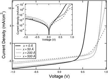 | ||
| Fig. 1 J–V curves obtained under 1 sun illumination for planar heterojunction devices with structures ITO/x Å MoO3/200 Å ClAlPc/400 Å C60/80 Å BCP/Al. The inset shows the corresponding dark current curves. | ||
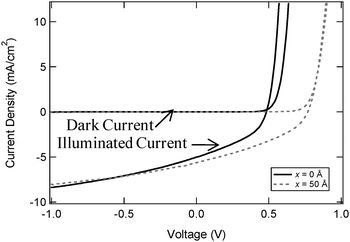
J–V curves for mixed heterojunction devices with the structure ITO/x Å MoO3/50 Å ClAlPc/500 Å (1:1 w/w) ClAlPc:C60/50 Å C60/80 Å BCP/Al, with x = 0 and 50 Å are shown in Fig. 2. At x = 0 Å, the device had a Jsc of 5.03 mA cm−2, a Voc of 0.48 V, a FF of 0.40 and a ηp of 1.0%. With x = 50 Å, Jsc and Voc both increased to 6.03 mA cm−2 and 0.76 V respectively and, although there is a small reduction in FF to 0.36, the overall ηp is increased to 1.7%. The primary benefit of mixed heterojunctions is an increase in the area of the donor–acceptor interface, which in turn improves the efficiency of exciton dissociation.14 However, random mixing also hinders charge transport which increases recombination losses.15 This is evident from the reduced FF in the devices employing the mixed photoactive layer. Notably, the increase in Voc upon insertion of a MoO3 interlayer is similar to that seen in the corresponding planar heterojunction devices. Table 1 provides a summary of the parameters obtained from both the planar and mixed layer device architectures.
 | ||
| Fig. 2
J–V curves in the dark and under 1 sun illumination for mixed heterojunction OPV devices with structures ITO/x Å MoO3/50 Å ClAlPc/500 Å 1:1 mix ClAlPc:C60/50 Å C60/80 Å BCP/Al. | ||
:1 mix ClAlPc:C60/500 Å C60/80 Å BCP/Al
| Device | V oc /V | J sc /mA cm−2 | J s /mA cm−2 | FF | η (%) |
|---|---|---|---|---|---|
| A: ITO (x = 0) | 0.51 ± 0.03 | 5.68 ± 0.20 | 6.3 × 10⁻⁵ | 0.57 ± 0.01 | 1.6 |
| B: ITO/MoO3 (x = 50 Å) | 0.82 ± 0.01 | 5.46 ± 0.10 | 7.4 × 10⁻⁵ | 0.58 ± 0.01 | 2.6 |
| C: ITO/MoO3 (x = 100 Å) | 0.81 ± 0.01 | 4.68 ± 0.10 | 6.4 × 10⁻⁵ | 0.58 ± 0.03 | 2.2 |
| D: ITO/MoO3 (x = 200 Å) | 0.81 ± 0.01 | 4.43 ± 0.05 | 5.7 × 10⁻⁵ | 0.56 ± 0.01 | 2.0 |
| E: ITO/MoO3 (x = 500 Å) | 0.81 ± 0.01 | 4.02 ± 0.05 | 9.2 × 10⁻⁵ | 0.55 ± 0.03 | 1.8 |
| F: ITO (x = 0) | 0.48 ± 0.01 | 5.03 ± 0.10 | 8.8 × 10⁻⁵ | 0.40 ± 0.03 | 1.0 |
| G: ITO/MoO3 (x = 50 Å) | 0.76 ± 0.01 | 6.03 ± 0.20 | 9.4 × 10⁻⁵ | 0.36 ± 0.01 | 1.7 |
For both the planar and mixed layer OPV devices, the significant increase in ηp upon incorporation of the 50 Å MoO3 layer at the ITO/ClAlPc interface is due to a large increase in Voc. This increase cannot be attributed to an increase in the effective band gap of the photoactive matrix, which is unchanged for devices with and without the MoO3 interlayer. The MoO3 layer has an IP of 5.3 eV8,16 which, in the absence of an induced interfacial dipole, is in close alignment with the HOMO of ClAlPc (∼5.3 eV),12 as shown in Fig. 3. This degree of alignment is consistent with the observation that the 50 Å thick MoO3 layer does not significantly deteriorate Jsc in the devices. The reason for the large increase in Voc must therefore arise from a change in the nature of the contact with the ITO electrode.
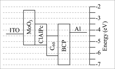 | ||
| Fig. 3 Electronic energy level diagram for the OPV devices ITO/MoO3/ClAlPc/C60/BCP/Al. | ||
Recently, Li et al. reported an improvement in the dark current characteristics for SnPc/C60 OPV devices containing a MoO3 layer,10 which offers a possible explanation for a change in Voc. The SnPc/C60 system was used in this instance due to its extraordinarily high dark current values, with the improvement in Voc shown to be directly proportional to ln(Jph/Js), where Js is the reverse dark saturation current and Jph is the photocurrent. However, in our ClAlPc/C60 system, the Jph and Js values are very similar both with and without the MoO3 interlayer since the system has very good dark current characteristics (as seen in Fig. 1 and the Js values in Table 1), so a different explanation is needed for the increase in Voc. We propose that the most probable reason for the increase in Voc is due to charge transfer from ITO to trap states at the ITO/MoO3 interface, pinning the ITO Fermi level to the valance band of MoO3, and giving a favourable vacuum level shift.17 This phenomenon would operate to increase the potential difference between electrons in the anode and cathode, thereby increasing Voc.
The addition of the MoO3 interlayer increases the series resistance (Rs) of the devices which can lead to lower Jsc and FF values.8,18 We found an optimal MoO3 thickness of 50 Å, with thinner layers (x < 50 Å) giving incomplete coverage of the ITO substrate, and thicker layers (x > 50 Å) resulting in decreased performance due to the increase in Rs. Fig. 1 and Table 1 show that for all MoO3 thicknesses above 50 Å the Voc remains constant at ∼0.82 V, consistent with the interfacial pinning hypothesis given above. The FF is reduced slightly from 0.58 for x = 50 Å to 0.55 for x = 500 Å, with Jsc also reduced from 5.68 mA cm−2 to 4.02 mA cm−2 due to the increases in series resistance with increasing MoO3 thickness. These results are in direct contrast to those recently published by Kinoshita et al.,9 who reported increased ηp in H2TPP/C60 planar heterojunction devices by increasing the MoO3 layer thickness at the H2TPP/ITO interface up to 500 Å.
Fig. 4 shows the AFM topography images (a,b) and KP-AFM images (c,d) of bare ITO and MoO3 covered ITO. AFM shows that the surface morphologies for ITO, ITO/MoO3 (50 Å) and ITO/MoO3 (50 Å)/ClAlPc (50 Å) are very similar, with the root mean square roughness, Rq, varying between 3.68 and 4.08 nm. This discounts any significant variation in surface morphology as a reason for the changed behaviour when introducing MoO3 into the devices. Using KP-AFM, the variation in work function can be seen across the ITO and the ITO/MoO3 surfaces. The MoO3 surface gives a smaller variation, with a root mean square deviation from the average work function of 9.9 mV in comparison to 13.6 mV for ITO. Insertion of the MoO3 interlayers was found to reduce variations in OPV device performance (Table 1), consistent with a decoupling of the photoactive layer from the electrically inhomogeneous ITO electrode.
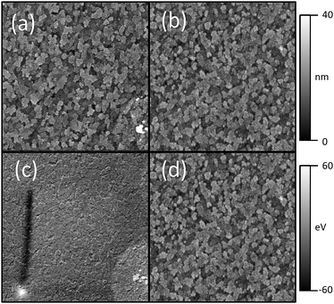 | ||
| Fig. 4 AFM topography images of (a) ITO and (b) ITO/MoO3 (x = 50 Å). Corresponding KP-AFM images of (c) ITO and (d) ITO/MoO3 (x = 50 Å). The topography images are both on a 0–40 nm scale. The KP-AFM images are on a −60 mV to 60 mV deviation from the average work function scale. All images have lateral dimension of 5 μm by 5 μm. | ||
The planar heterojunction ClAlPc/C60 devices with x = 0 and 50 Å MoO3 were also tested under constant illumination for 1 h under a nitrogen atmosphere. Table 2 shows the percentage degradation of each key device parameter from the value at 0 min to 60 min. Devices containing a 50 Å MoO3 layer had significantly less degradation than those on bare ITO (8% compared to 46%). The largest improvement when inserting a 50 Å MoO3 layer is the stability of the Voc for the device, with only 2% degradation for each, in comparison to 35% for devices on bare ITO. Improvements were also seen in Jsc and FF. We believe this is due to the MoO3 interlayer preventing damage caused to the ClAlPc at the ITO/ClAlPc interface, which would otherwise reduce charge transport and could lead to a build up of charges, increasing the degradation of device performance.
| Device | V oc (%) | J sc (%) | FF (%) | η (%) |
|---|---|---|---|---|
| 0 Å | 35 | 16 | 4 | 46 |
| 50 Å | 2 | 6 | 0 | 8 |
In summary, we have shown that insertion of a very thin MoO3 hole-extracting layer leads to significant improvements (60–70%) in the power conversion efficiency of both planar and mixed heterojunction OPVs based on ClAlPc/C60 heterojunctions. The improvements are due to an increase in the Voc, which we propose results from pinning of the ITO Fermi level to the valance band of the MoO3 interlayer, where the latter is closely aligned with the highest occupied molecular orbital of ClAlPc. Insertion of the MoO3 layers also minimises variations in device performance by decoupling the photoactive layer from the electrically inhomogeneous ITO electrode. It also leads to a far greater device stabilisation, which is often overlooked when measuring device performance.
Acknowledgements
This work was supported by the Engineering and Physical Sciences Research Council (EPSRC), UK, under the SuperGen Excitonic Solar Cell Consortium. RAH is grateful to the Royal Academy of Engineering/EPSRC for the award of a Fellowship.Notes and references
- B. P. Rand, J. Genoe, P. Heremans and J. Poortmans, Progr. Photovolt.: Res. Appl., 2007, 15, 659 Search PubMed.
- M. Riede, T. Mueller, W. Tress, R. Schueppel and K. Leo, Nanotechnology, 2008, 19, 424001 CrossRef.
- C. W. Tang, Appl. Phys. Lett., 1986, 48, 183 CrossRef CAS.
- P. Sullivan and T. S. Jones, Org. Electron., 2008, 9, 656 CrossRef CAS.
- P. Sullivan, S. Heutz, S. M. Schultes and T. S. Jones, Appl. Phys. Lett., 2004, 84, 1210 CrossRef CAS.
- P. Peumans, V. Bulovic and S. R. Forrest, Appl. Phys. Lett., 2000, 76, 2650 CrossRef CAS.
- C. Uhrich, D. Wynands, S. Olthof, M. K. Riede, K. Leo, S. Sonntag, B. Maennig and M. Pfeiffer, J. Appl. Phys., 2008, 104, 043107 CrossRef.
- V. Shrotriya, G. Li, Y. Yao, C. W. Chu and Y. Yang, Appl. Phys. Lett., 2006, 88, 073508 CrossRef.
- Y. Kinoshita, R. Takenaka and H. Murata, Appl. Phys. Lett., 2008, 92, 243309 CrossRef.
- N. Li, B. E. Lassiter, R. R. Lunt, G. Wei and S. R. Forrest, Appl. Phys. Lett., 2009, 94, 023307 CrossRef.
- R. F. Bailey-Salzman, B. P. Rand and S. R. Forrest, Appl. Phys. Lett., 2007, 91, 013508 CrossRef.
- S. W. Cho, L. F. J. Piper, A. DeMasi, K. E. Smith, K. V. Chauhan, P. Sullivan, R. A. Hatton and T. S. Jones, J. Phys. Chem. C Search PubMed , submitted.
- R. F. Salzman, J. Xue, B. P. Rand, A. Alexander, M. E. Thompson and S. R. Forrest, Org. Electron., 2005, 6, 242 CrossRef CAS.
- P. Peumans, A. Yakimov and S. R. Forrest, J. Appl. Phys., 2003, 93, 3693 CrossRef CAS.
- L. J. A. Koster, V. D. Mihailetch and P. W. M. Blom, Appl. Phys. Lett., 2006, 88, 052104 CrossRef.
- C. Tao, S. Ruan, X. Zhang, G. Xie, L. Shen, X. Kong, W. Dong, C. Liu and W. Chen, Appl. Phys. Lett., 2008, 93, 193307 CrossRef.
- H. Ishii, K. Sugiyama, E. Ito and K. Seki, Adv. Mater., 1999, 11, 605 CrossRef CAS.
- M. Y. Chan, C. S. Lee, S. L. Lai, M. K. Fung, F. L. Wong, H. Y. Sun, K. M. Lau and S. T. Lee, J. Appl. Phys., 2006, 100, 094506 CrossRef.
| This journal is © The Royal Society of Chemistry 2010 |