Preparation, structure and properties of Mn-doped ZnO rod arrays
Dianwu
Wu
a,
Zhongbing
Huang
*a,
Guangfu
Yin
a,
Yadong
Yao
a,
Xiaoming
Liao
a,
Dong
Han
b,
Xia
Huang
b and
Jianwen
Gu
*c
aCollege of Materials Science and Engineering, Sichuan University, Chengdu, 610065, China. E-mail: zbhuang@iccas.ac.cn.; Fax: +86-28-85413003; Tel: +86-28-85413003
bZhengzhou Research Institute, Aluminum Corporation of China Limited, Zhengzhou, China
cThe Military General Hospital of Chengdu PLA, Chengdu, China. E-mail: gujianwen5000@yahoo.com.cn; Tel: +86-28-86570362, 86570361
First published on 28th August 2009
Abstract
Mn-doped ZnO rod arrays were successfully prepared on zinc substrate by a simple aqueous solution method. X-Ray diffraction and high resolution transmission electron microscopy results indicate the doped Mn2+ has successfully incorporated into the ZnO crystal lattice. The optical, magnetic and electrical properties of as-prepared ZnO rod arrays were all changed due to Mn2+ doping into ZnO rods. Photoluminescence spectra at room temperature suggest that the band gap increases with increasing the Mn concentrations in ZnO rods. The M–H curves of all Mn-doped ZnO rod arrays show obvious ferromagnetic characteristics at room temperature. The current–voltage characteristic curves of Mn-doped ZnO rod arrays indicate that the samples are typical semiconductors.
1 Introduction
Zinc oxide (ZnO) is one of the multifunctional semiconductor materials which have a wide band gap and large exciton binding energy that ensures significant excitonic emission at room temperature. Its properties have been studied for many years and the research in the morphology and optical, magnetic, and electrical properties of ZnO is significant for basic applications including low-voltage and short-wavelength electro-optical devices, transparent ultraviolet protection films, and gas sensors.1–4 Different methods have been reported for the synthesis of well-aligned nanorod,5–7 nanowire,8,9 nanotube,10,11 and nanobelt12,13 arrays. The aqueous solution method is preferred due to its convenience and low cost. However, a doped ZnO nanostructure by a controllable method is difficult to prepare.14,15 Most of the researchers reported that they had difficulties in controlling the structure and the composition of the doped ZnO nanowire or nanorod arrays. It is well known that doping a selective element into ZnO has become an important route to improve the optical, magnetic properties, and to increase the carrier concentration for electronic applications because a higher carrier concentration is required. Recently, many studies focus on the transition metal (TM) such as Mn, Ni, Fe, Co and Cr doped into ZnO due to their potential applications in spintronics.16 However, there are a great deal of controversy about whether TM-doped ZnO has room temperature ferromagnetism, and research on the electrical properties of Mn-doped ZnO arrays has scarcely been reported, which could limit the applications of ZnO arrays.In this article, we successfully prepared Mn-doped ZnO rod arrays on zinc substrate, controlling their Mn concentration by a simple aqueous solution method. The optical, magnetic, and electrical properties of as-prepared ZnO rod arrays were all changed with the change of Mn concentrations. Moreover, ZnO materials are believed to be non-toxic, biosafe and biocompatible,17 and have been used in many applications of daily life, such as drug carriers, cosmetics and fillings in medical materials.18,19 Based on these properties, the prepared ZnO rod arrays have the possibility of being applied for biological nanodevices to detect several diseases or bacteria.
2 Experimental
2.1 Materials
Zinc foil (the volume is 30 × 10 × 0.4 mm3), zinc nitrate (Zn(NO3)2·6H2O (A.R.), hexamethylenetetramine (C6H12N4, HMT, A.R., Kelong chemical reagent plant of chengdu, China) and manganese acetate (Mn(CH3COO)2·4H2O, A.R. Kemiou chemical reagent development center of tianjin, China) were used for the preparation of ZnO rod arrays.2.2 Preparation of Mn-doped ZnO rod arrays
The experiment was conducted using the following procedure. Mn-doped ZnO rod arrays were grown vertically by immersing zinc substrate in the aqueous solution of equimolar C6H12N4 (HMT) and Zn(NO3)2·6H2O (25 µ L−1), and different concentrations of Mn(CH3COO)2·4H2O. The dopant concentrations in the reactive solution were 0, 2.5, 5.0, 7.5, 10 µ L−1, to result in Mn/Zn ionic of 0, 0.1, 0.2, 0.3, and 0.4, respectively, and the as-prepared samples in the subsequent discussion in this paper are referred to as C0, C1, C2, C3 and C4, respectively. The growth time and temperature were 12 h and 80 °C, respectively. Finally, the as-prepared samples were removed from the solution, rinsed thoroughly 5 times with deionized water to remove residual salts, and dried for 24 h at room temperature.To characterise the electrical properties of as-prepared ZnO rod arrays, an I-V measurement was performed on zinc substrate, where one electrode contacted zinc and the other one was in contact with ZnO rod arrays. In order to give a contrast between macroscopic and microcosmic electrical properties of ZnO rod arrays, we choose brass wire and AFM tip (Pt) to be the contact electrode, respectively. Scheme 1 shows a schematic illustration of the experiment of electrical properties setup. The zinc foil was not only used for providing a zinc-ion source for the growth of ZnO particles but was also used as the conductive channel. The brass wire tip, which was used for forming the gateway, was ground into the coniform.
 | ||
| Scheme 1 Schematic diagram of the experimental setup. The contact electrodes are (a) brass wire, and (b) Pt tip, respectively. | ||
2.3 Characterization
The morphology and crystalline structures of Mn-doped ZnO rod arrays were studied by high-resolution transmission electron microscopy (HRTEM, JEM-2200, Japan) and accompanying selected area electron diffraction (SAED), scanning electron microscopy (SEM, JSM-5900LV, Japan), an X-ray diffractometer (X'Pert, Holand) with Cu Kα radiation, respectively. Analysis of the elements was conducted using energy-dispersive X-ray spectroscopy (EDX) coupled with HRTEM. The photoluminescence (PL) measurements were performed on a Hitachi F-7000 Fluorometry with a Xe lamp as the excitation light source at room temperature. The ferromagnetic behavior of the samples at room temperature was investigated by vibrating sample magnetometer (VSM, Lake shore-7400, USA). Their current–voltage characteristics were investigated by an electrochemistry analysis system (LK9805, China) and atomic force microscopy (AFM, Aligent 5500, USA).3 Results and discussion
The morphology of undoped ZnO rod arrays (C0 sample) grown on zinc substrate was shown in Fig. 1. Hexagonal ZnO rods with an average diameter of about 500 nm and a length of about 4.5 µm, are grown perpendicular to the zinc surface to form large-scale nearly uniform arrays. Fig. 2 shows SEM images of ZnO rod arrays doped with different Mn concentrations. The average diameters of as-prepared ZnO rods are about 350, 350, 400 and 500 nm for C1, C2, C3 and C4, respectively, indicating that the diameter of the ZnO rod is changed with increasing the Mn concentrations according to EDX results. The corresponding crow-view images indicate that the length of doped rod arrays, about 4 mm, is slightly smaller than that of the C0 sample. | ||
| Fig. 1 SEM image of the side view of undoped ZnO rod arrays. | ||
 | ||
| Fig. 2 SEM images of ZnO rod arrays grown with different dopant concentrations in reactive solutions. (a) C1. (b) C2. (c) C3. (d) C4. The insets are cross-view images of the obtained samples. | ||
In order to determine the structure of ZnO rod arrays, XRD was performed. Fig. 3 displays XRD patterns of the as-prepared undoped and doped ZnO samples. All ZnO diffraction peaks are in good agreement with the JCPDS card (No. 36-1451) for a typical wurtzite-type ZnO crystal (hexagonal). These peaks at scattering angles (2θ) of 34.478, 36.537, 39.076, 47.392, and 62.925° correspond to the diffractions from the 100, 002, 101, 102, and 103 crystal planes of the ZnO hexagonal phase, respectively. The (002) diffraction peaks of Mn-doped ZnO rod array, compared to undoped ZnO rod arrays, left-shift by about 0, 0.2, 0.2 and 0° for C1, C2, C3, and C4, respectively. The c-axis lattice parameter decreased with the dopant incorporated into the crystal lattice. Because of the larger radius of Zn2+ (0.74 Å)20 as compared to that of Mn2+ (0.66Å), the replacement of some Zn2+ by Mn2+ will cause a slight decrease in the lattice parameters. No other diffraction peaks were detected, except for the peaks originating from the zinc substrate (marked with a square in Fig. 3), implying that there was no MnO or MnO2 crystal in the doped arrays.
 | ||
| Fig. 3 XRD patterns of the prepared undoped and Mn-doped ZnO rod arrays. | ||
In order to further determine the structure and composition of doped ZnO samples, HRTEM was performed due to the probability that a secondary phase might exist in our samples too small to be detected by the XRD results. Fig. 4 clearly shows that no other phase was observed except for the rod-like ZnO, indicating that Mn2+ has been successfully incorporated into the ZnO crystal lattice. The HRTEM image in Fig. 4b shows the 2.6 Å {001} lattice fringe parallel to the basal plane. It provides further confirmation that the rods were growing along [001] direction.
 | ||
| Fig. 4 (a) TEM image of a doped ZnO rod arrays doped C3 sample, the inset is a selected area of electron diffraction taken from a fine ZnO rod; (b) HRTEM image of the sample. | ||
The composition of C3 is determined by EDX (Fig. 5), and the result shows the existence of Mn, Zn, O, Cu and C in the spectrum. The elements Cu and C are ascribed to the copper web and organic film, respectively, which were used for TEM. It suggests that Mn has entered the ZnO rod arrays. Table 1 shows the Mn percentage in doped ZnO rod arrays determined by EDX. There are 3 and 6% Mn ions doped into ZnO rods of samples C2 and C3, respectively. In addition, the actual quantities of Mn2+ in samples C1 and C4 are too small to be quantificationally detected by EDX.
| Sample | C1 | C2 | C3 | C4 |
|---|---|---|---|---|
| Mn% in rod | < 1 | 3 | 6 | <1 |
 | ||
| Fig. 5 EDX of a Mn-doped ZnO single rod (C3 sample). | ||
Obviously, the amount of Mn incorporated into the ZnO matrix is far less than the amount of Mn provided in the reaction solution. Due to the higher bond energy of Mn–O as compared to that of Zn–O, more energy is required to enable Mn2+ to enter the lattice and form the Mn–O bond. Therefore, Mn2+ substituting for Zn2+ has a higher stability than the Zn–O structure, and more energy is required in the substituted samples to form the Zn–O–Mn structure.
It is well known from the synthesis of particles that the dopant atoms have a strong influence on the amount and size of the resulting rods21–23 due to a kinetic equilibrium process of the thermodynamic and dynamic equilibria. The high concentration of dopants would be nucleated with oxygen ions by itself and grow up due to the kinetic equilibrium. Thus, it would be difficult for Mn2+ to be incorporated into ZnO in its high concentration.
We discuss the growth mechanism of ZnO rod arrays on Zn foil. In the first step, Zn foil would be readily oxidized to form a compact thin film, including a lot of ZnO nanoparticles in high temperature solution. These ZnO nanoparticles become the nuclei for further ZnO crystal growth. ZnO has the natural tendency for anisotropic growth along the crystalline c-axis,24,25 and the high temperature solution serves as a kinetic driving force and promotes the anisotropic development and thus the growth of elongated rods. As a result, ZnO rod arrays on Zn substrate are formed. Fig. 4a shows a TEM image of sample C3. Obviously, the rods in the array are broken into fine-rods by ultrasonic vibration and the average diameter of the fine-rods is less than 100 nm. However, according to the SEM image of C3 (Fig. 2c), the average diameter of many ZnO rods is less than 300 nm, indicating that one large doped ZnO rod is composed of several fine doped ZnO rods clinging to each other. It is believed that fine diameter rods grow as a bundle individually initially and coalesce eventually to form large-diameter rods that can lower their surface energy.26,27 In a reaction temperature of 80 °C, a high concentration of alkali (due to lower evaporation at 80 °C) might have resulted in doped ZnO rods with a large diameter of 300 nm. Furthermore, the higher bond energy of Mn–O could also promote coalescence between fine doped rods and lead to the formation of large-diameter rods. According to our experimental results, the proposed growth mechanism of a wurtzite-type doped ZnO crystal is as-follows, the first step is the growth process of the fine doped ZnO rods but they are independent (shown in Fig. 4a), and then the second step is the growth steps of hexagonal rods of doped ZnO via the coalescence mode, the last step is a result of a larger irregular rod (shown in Fig. 2).
The PL spectra (Fig. 6) consist of an UV emission peak which is centered at 390 nm, a distinct peak centered at 465 nm, and a weaker green emission band centered at 530 nm, respectively. The UV luminescence band (390 nm) belongs to the exciton recombination corresponding to near-band-edge emission of the ZnO rod.28 The position of each sample's UV-emission peak was marked in the spectra with arrows, and it can be clearly observed that the UV-emission peaks were blue-shifted by 4.78, 6.44, 10.21, and 4.05 nm for C1, C2, C3, and C4 compared to C0, respectively. This indicates that the band gap increases with increasing the doping Mn concentrations. With the increase of Mn concentration in ZnO, the peaks of UV-emission are getting stronger. The improved near-band-edge intensity can be understood from the following aspects: the larger band gap of the MnO compared to that of ZnO more efficiently confines the electrons/holes in the ZnO rods, and their recombination pairs give the near band edge emission. The green emission peaks have been reported to be ascribed to the oxygen vacancies (VO) and the transition of a photogenerated electron from a dark level below the conduction band to a deeply trapped hole.29
 | ||
| Fig. 6 PL spectrum of different Mn-doped ZnO rod arrays grown on zinc substrate measured at room temperature. The excitation wavelength of PL is the 310 nm. | ||
The ferromagnetic behavior of Mn-doped ZnO rod arrays was investigated through measuring the magnetization (M) vs magnetic field (H) curves. As shown in Fig. 7, the M–H curves of all Mn-doped ZnO rod arrays at room temperature obviously show ferromagnetic characteristics. Their coercivities (Hc) are 200, 220, 300, and 250 Oe for C1, C2, C3, and C4, respectively (shown in the insets of Fig. 8). The saturation magnetizations (MS) of Mn-doped ZnO arrays are up to 0.05, 0.13, 0.26, and 0.03 emu g−1, respectively. The saturation magnetizations we measured are larger than the previous reports on Mn-doped ZnO nanocrystals.30 However, it is less than our result for Ni-doped ZnO rod arrays.23 Ferromagnetism is enhanced significantly with increasing the Mn2+ concentrations in ZnO. It is noted that a secondary phase (manganese oxides) does not exist in the Mn-doped ZnO rod arrays according to our XRD and HRTEM results. Manganese oxides (such as MnO and MnO2) are well known to be antiferromagnetic below the Neel temperature of 116 and 84 K, respectively.31 Instead of generating carriers, the addition of Mn2+ into Zn sites would influence the electronic band structure of the materials, and we ascribe ferromagnetism in Mn-doped ZnO samples to the fact that the conduction band is hybridizing with some of the d electrons of the transition metal dopant. Thus, it is the doping Mn ions that drive the magnetism in these samples.
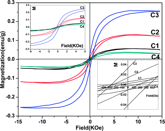 | ||
| Fig. 7 Magnetic hysteresis loops of Mn-doped ZnO rod arrays at room temperature, the insets show its enlarged view at the origin and at zero field, respectively. | ||
 | ||
| Fig. 8 (a) I–V curves corresponding to different concentrations of Mn-doped ZnO rod arrays from −3 to 3 V with a Cu contact electrode. The inset shows I–V curve of undoped ZnO rod arrays. (b) I–V curve of different dots of C3 sample in the range of −3 to 3 V with Pt contact electrode. The inset shows AFM images of the different measured dots. | ||
Fig. 8a shows I–V curves of different concentrations of Mn-doped ZnO rod arrays from −3 to 3 V with copper contact electrode (the tip diameter of the copper wire is about 20 µm). The electron affinity of ZnO is 4.5 eV32 and the work function of Cu, Zn and Pt is 5.10, 3.63 and 6.1 eV, respectively.33 A barrier may exist at the interface between metal and semiconductor and the I–V characteristic of the system is Schottky. Obviously, the current in the anode from Fig. 8 is restrained and a barrier may exist at the interface between metal and semiconductor. From Scheme 1 the anode is a metal and the cathode is a semiconductor. The semiconductor has more free electrons as compared to the metal, so the electrons will diffuse from the semiconductor (high concentrations of electrons) to the metal (lower concentrations of electrons). This shows that our prepared materials are n-type semiconductors. In these curves, undoped ZnO rod arrays have a lower conductance (shown in the inset of Fig. 8a), and the current becomes strong with increasing Mn2+ concentration in reactive solution, followed by a decrease when the concentration in solution is up to 40%. Thus, the actual quantity of Mn2+ incorporated into the ZnO crystal lattice may play an important role.
Fig. 8b shows a I–V curve of Mn-doped ZnO rod arrays (sample of C3) with Pt contact electrode (the tip diameter of Pt is about 20 nm). All curves are nonlinear, indicating that the contacts between rod and Pt electrode are not ideally ohmic. The current is more than −100 nA when the voltage is up to −3 V in Fig. 8b. However, the current in Fig. 9a, which was measured with copper as the contact electrode, was nearly 150 times the current in Fig. 8b. The diameter of the copper wire is about 20 µm and the average diameter of ZnO rods is 300 nm. When copper wire touches ZnO rod arrays, a great number of rods must simultaneously contact the copper wire. Another copper wire contacted with zinc substrate can be considered as the connecting electrode and they can form a parallel connection by thousands of rods. The total resistance should be thousands of times that of the single rod. However, only about 150 times of the current difference was found between Fig. 8a and Fig. 8b. This may be explained as followed: the as-prepared ZnO rod arrays are not uniform in their height, and the copper wire can just touch part of the rods. Moreover, the formation of a metal-semiconductor has a function of the current magnification.
 | ||
| Fig. 9 Sketch of d states of Mn splitting, influenced by the crystal field of ZnO. | ||
It is well known that the intrinsic defects, the diameter of the rods, the interplay between the electron orbits of Mn-doped ZnO may be the reasons that the current becomes strong with increasing Mn2+ concentration. Philipose et al34 have reported that the large carrier concentration observed was probably due to a large concentration of intrinsic defects, which was confirmed by strong green luminescence. However, the intensities of the weak green luminescence in PL measurements are almost not changed, confirming that the affection of intrinsic defects might be negligible. Fig. 8b shows a I–V curve of different rods in Mn doped ZnO rod arrays (sample of C3), and the inset shows an AFM image of the different measured rods. Obviously, the size of rod 2 is larger than that of rod 1, and comparing the current of the two rods shows that the current will turn stronger with increasing the diameter of the rods, which can be explained using the “continuous surface” model.35 Moreover, rod 3 is not alone and has a stronger current, revealing that lots of rods adhering to each other could enhance their current. This is in good agreement with the growth mechanism of the ZnO rod arrays, and that one large ZnO rod could be composed by several small ZnO rods clinging to one another, resulting in the increase of the current.
Generally, the electron was the majority carrier in an n-type semiconductor. However, the substitution of Mn into ZnO (MnZn) should not contribute shallow donor or acceptor levels, since the outer shell of Mn is isoelectronic with Zn. The current becomes strong with increasing Mn2+ concentration in ZnO rods, so where the do the electrons come from? The influence of the electrons in the hypo-outer shell of Mn should be taken into account. The large current can be understood from the following aspects: the hypo-outer shell of Mn is the d states which generally appear near the Fermi level (Fig. 9). These d states are likely to split and the splitting of a corresponding d state may result in the high-spin configuration of d electrons. These d states hybridize with valence p states of ZnO. In our samples, Mn2+ partially substitutes Zn2+ in ZnO, and the Zn ion locates at the center of the tetrahedron made of four oxygen atoms. The d states of Mn may be influenced by the tetrahedral crystal field of ZnO and split into a higher energy triplet state and a lower doublet state. The triplet state subsequently hybridizes with the p orbital of the valence band and further splitting into the bonding states and antiboding states. The bonding states participate in the bonding (Mn–O) and are hence localized. However, the antibonding states have a higher energy level and contain some itinerant electrons. The high energy of the antibonding state is very close to the conduction band and the electrons in this state have a higher probability of jumping to the conduction band. Due to the increase of Mn concentration in ZnO rods, more electrons are possible to be promoted to the conduction band, resulting in further increase of conductivity. This is the reason that the current becomes strong with increasing the Mn2+ concentration in ZnO rods.
4 Conclusions
Mn-doped ZnO rod arrays have been successfully synthesized by a simple aqueous solution route. The as-prepared products are a single-crystalline wurtzite structure, and Mn2+ has been successfully incorporated into the ZnO crystal lattice. The optical, magnetic, and electrical properties of Mn-doped ZnO rod arrays have been discussed, and particularly important features are as follows: PL spectra demonstrate that the band gap of ZnO rod arrays have changed with increasing the Mn concentrations in ZnO rods, all Mn-doped ZnO rod arrays show obvious ferromagnetic properties at room temperature. The analyses from the I–V characteristic suggest that as-prepared ZnO rod arrays are n-type semiconductor. These ZnO rod arrays can be applied in electrical products and for detecting diseases and bacteria.Acknowledgements
This work was supported by the National Natural Science Foundation of China (project No. 60871062 and 50873066). Support by Sichuan Province through a Science Fund for Distinguished Young Scholars of Sichuan Province (08ZQ026-007), Key Technologies Research and Development Program of Sichuan Province (2008SZ0021 and 2006Z08-001-1) and the Research Fund for the Doctoral Program of Higher Education from Ministry of Education of China (No. 20070610131) is also acknowledged with gratitude. We thank the Analytical & Testing Center, Sichuan University for assistance with the microscopy work. Thanks are also due to Mrs Hui Wang from the Analytical & Testing Center, Sichuan University, for her constant instruction.Notes and references
- S. Lenfant, C. Krzeminski, C. Delerue, G. Allan and D. Vuillaume, Nano Lett., 2003, 3, 741 CrossRef CAS.
- Z. Wei, M. Kondratenko, L. H. Dao and D. F. Perepichka, J. Am. Chem. Soc., 2006, 128, 3134 CrossRef CAS.
- W. I. Park, Y. H. Jun, S. W. Jung and G. C. Yi, Appl. Phys. Lett., 2003, 82, 964 CrossRef CAS.
- X. Duan, Y. Huang, R. Agarwal and C. W. Lieber, Nature, 2003, 421, 241 CrossRef CAS.
- Y. X. Wang, X. Y. Li, G. Lu, X. Quan and G. H. Chen, J. Phys. Chem. C, 2008, 112, 7332 CrossRef CAS.
- G. Wang, D. Chen, H. Zhang, J. Z. Zhang and J. Li, J. Phys. Chem. C, 2008, 112, 8850 CrossRef CAS.
- S. K. Panda, A. Dev and S. Chaudhuri, J. Phys. Chem. C, 2007, 111, 5039 CrossRef CAS.
- Y. Qin, R. Yang and Z. L. Wang, J. Phys. Chem. C, 2008, 112, 18734 CAS.
- L. E. Greene, M. Law, D. H. Tan, M. Montano, J. Goldberger, G. Somorjai and P. Yang, Nano Lett., 2005, 5, 1231 CrossRef CAS.
- L. Li, S. Pan, X. Dou, Y. Zhu, X. Huang, Y. Yang, G. Li and L. Zhang, J. Phys. Chem. C, 2007, 111, 7288 CrossRef CAS.
- Q. Li, V. Kumar, Y. Li, H. Zhang, T. J. Marks and R. P. H. Chang, Chem. Mater., 2005, 17, 1001 CrossRef CAS.
- T. Sun, J. Qiu and C. Liang, J. Phys. Chem. C, 2008, 112, 715 CrossRef CAS.
- G. Z. Shen, Y. Bando and D. Golberg, J. Phys. Chem. C, 2007, 111, 5044 CrossRef CAS.
- P. V. Radovanovic and D. R. Gamelin, J. Am. Chem. Soc., 2001, 123, 12207 CrossRef CAS.
- D. A. Schwartz, N. S. Norberg, Q. P. Nguyen, J. M. Parker and D. R. Gamelin, J. Am. Chem. Soc., 2003, 125, 13205 CrossRef CAS.
- C. Bauer, G. Boschloo, E. Mukhtar and A. Hagfeldt, J. Phys. Chem. B, 2001, 105, 5585 CrossRef CAS.
- J. Zhou, N. S. Xu and Z. L. Wang, Adv. Mater., 2006, 18, 2432 CrossRef CAS.
- M. Ito, Biomaterials, 1991, 12, 41 CrossRef CAS.
- D. Orstavik and J. K. Hongslo, Biomaterials, 1985, 6, 129 CrossRef CAS.
- Y. Miyake and H. Tada, J. Chem. Eng. Jpn., 2004, 37, 630 CrossRef CAS.
- S. Pearton, W. Heo, M. Ivill, D. Norton and T. Steiner, Semicond. Sci. Technol., 2004, 19, R59 CrossRef CAS.
- S. Chambers, T. Pronbay, C. Wang, K. Rossa, S. Heald, D. Schwartz, K. Kittilstved and D. Gamelin, Mater. Today, 2006, 9, 18 CrossRef CAS.
- D. Wu, M. Yang, Z. Huang, G. Yin, Y. Yao, X. Liao, Y. Kang, X. Chen and H. Wang, J. Colloid Interface Sci., 2009, 330, 380 CrossRef CAS.
- L. Vayssieres, K. Keis, S. Lindquist and A. Hagfeildt, J. Phys. Chem. B, 2001, 105, 3350 CrossRef CAS.
- L. Vayssieres, G. Yi, M. Kim and S. Lindquist, Chem. Mater., 2001, 13, 4395 CrossRef CAS.
- Z. Huang, Y. Zhu, S. Wang and G. Yin, Cryst. Growth Des., 2006, 6, 8.
- P. Zhang, F. Xu, A. Navrotsky, J. Lee, S. Kim and J. Liu, Chem. Mater., 2007, 19, 5687 CrossRef CAS.
- J. J. Wu and S. C.Liu, Adv. Mater., 2002, 14, 215 CrossRef CAS.
- C. G. Kim, K. Sung, T. M. Chung, D. Y. Jung and Y. Kim, Chem. Commun., 2003, 2068 RSC.
- K. C. Barick, M. Aslam, V. P. Dravid and D. Bahadur, J. Phys. Chem. C, 2008, 112, 15163 CrossRef CAS.
- S. W. Jung, S. J. An, G. C. Yi, C. U. Jung, S. I. Lee and S. Cho, Appl. Phys. Lett., 2002, 80, 24.
- S. Hasegawa, S. Nishida, T. Yamashita and H. Asahi, J. Ceram. Process.Res., 2005, 6, 245 Search PubMed.
- H. B. Michaelson, J. Appl. Phys., 1977, 48, 4729 CrossRef CAS.
- U. Philipose, S. V. Nair, C. F. Trudel, S. Souza, R. H. Aouba and H. E. Ruda, Appl. Phys. Lett., 2006, 88, 263101 CrossRef.
- A. Motayed, Mark. Vaudin, A. V. Davydov, J. Melngailis, M. He and S. N. Mohammad, Appl. Phys. Lett., 2007, 90, 04310.
| This journal is © The Royal Society of Chemistry 2010 |