Surface micropatterning technique for surface-enhanced Raman scattering analysis†
Weidong
Ruan
ab,
Zhicheng
Lu
b,
Tieli
Zhou
b,
Bing
Zhao
*b and
Li
Niu
*a
aEngineering Laboratory for Modern Analytical Techniques, w/o State Key Laboratory of Electroanalytical Chemistry, Changchun Institute of Applied Chemistry, Changchun, 130022, P. R. China. E-mail: lniu@ciac.jl.cn; Fax: +86 431 85262800; Tel: +86 431 85262425
bState Key Laboratory of Supramolecular Structure and Materials, Jilin University, Changchun, 130012, P. R. China. E-mail: zhaobing@mail.jlu.edu.cn
First published on 9th April 2010
Abstract
A facile and powerful method to form micropatterns, based on nanosphere lithography and layer-by-layer self-assembly, is described in this paper. A monolayer of hexagon close-packed polystyrene (PS) spheres (av 600 nm) was employed as the template. A positively charged polyelectrolyte of poly(diallydimethylammonium) chloride was used as adhesive to absorb oppositely charged spherical Au (av 17 nm) and spherical Ag (av 12 nm), respectively. Both the PS and substrates were coated by colloidal nanoparticles. After removal of the PS template, a micropatterning surface was obtained. Scanning electron microscopy and atomic force microscopy were used to characterize the morphologies. These resulting patterns can be used as good surface-enhanced Raman scattering (SERS) substrates. The enhancement factor is calculated to be 104 ∼ 105. This is a simple and facile technique for surface modification of metal micropatterns with SERS analytical application.
1. Introduction
The preparation of nanostructured surfaces on materials with defined composition and morphology is of immense scientific and technological interest. Polyelectrolyte is a promising surface-modification reagent or adhesive which has been applied for a broad range of surface synthesis and self-assembly. Because the polyelectrolyte films can be tuned with desired composition and thickness, can be deposited onto different substrates with predetermined morphologies, and are versatile to adsorb different kinds of nanoparticles, a variety of polyelectrolyte coatings with unique properties such as electrical catalysis,1,2 anticorrosion,3 drug delivery4,5 and biosensors,6,7 have been synthesized.Currently there is great interest in the synthesis and application of more complex polyelectrolyte structures with periodic patterns by employing template techniques. Hammond et al.8,9 achieved selective depositions of polyelectrolytes on templates through inductive and prohibitive electrostatic forces. Following this work, they also prepared organic molecules and nanoparticles micro/nanopatterns on self-assembly ultrafilms functionalized by electrostatic interaction of positive or negative charges.10–12 Cui et al.13 demonstrated a photo-lithographic approach, which generated patterns on wafers by employing layer-by-layer (LbL) self-assembly of nanoparticles on desired locations. This work enabled the potential for industrial applications on microelectronics. The combination of LbL self-assembly and template techniques is a powerful way for constructing patterning surfaces, which have vast applications in both science and technology.14
Among all the template techniques, the colloidal crystal is a well-known one which has been used successfully in applications of macroporous materials,15,16 periodic patterns14,17 and photonic crystals.18,19 Polystyrene (PS) spheres are one of the general building blocks for the colloidal crystal. Using PS monolayer as the template, a great deal of micro/nanopatterns was constructed. This template technique, known as nanosphere lithography (NSL), was firstly introduced by Van Duyne in 1995.17 As a low-cost and commonly-used nanofabrication technique, NSL had intensive applications in surface plasmon resonance (SPR), local surface plasmon resonance (LSPR) and surface-enhanced Raman scattering (SERS).20–22 However, this template was rarely used in the field of electrostatic LbL self-assembly of nanoparticles. Correa-Duarte et al.23 deposited carbon nanotubes (CNTs) on a PS monolayer and prepared CNT/polymer thin films with periodic patterns. It is a quite convenient method for preparing polymer composite film with a unique distribution of CNTs inside a polymer matrix. Nanosensors were envisioned as a specific application for such structures because of their tunable electronic and optical properties.
In this work, we focused on the combination of NSL and LbL self-assembly, and intended to explore the SERS analytical application. Firstly, PS monolayer templates were employed. Secondly, polyelectrolyte and noble metal nanoparticles were deposited on the templates via electrostatic LbL self-assembly. Lastly, their SERS analytical application was examined. This is a facile and powerful method for fabricating micro-coatings with periodic structures for SERS application. After this surface modification, the substrate surfaces were brought to bear a SERS activity. Furthermore, only parts of the substrate surfaces were coated. The other part preserves the intrinsic surface character of the substrates maximally. It is an ideal method for the surface modification and SERS analysis.
2. Experimental section
2.1. Reagents
Hydrogen tetrachloroaurate (III) trihydrate (HAuCl4·3H2O, 99.9%) and silver nitrate (AgNO3, 99.8%) were purchased from Beijing Chemical Reagent Co., Ltd. Poly(diallydimethylammonium) chloride (PDDA) with medium molecular weight (200,000–350,000), sodium borohydride (NaBH4, 99%), trisodium citrate dihydrate (HOC(COONa)(CH2COONa)2·2H2O, 99%), and 4-aminothiophenol (4-ATP) were purchased from Sigma-Aldrich Chemical Co., Inc. The other chemicals (anhydrous ethanol, acetone, chloroform, H2SO4 98%, and H2O2 30%) were all reagent grade and obtained from Beijing Chemical Plant. All chemicals were used without further purification. Ultrapure water (>18 MΩ) purified with Milli-Q plus system (Millipore Co.) was exclusively used in all aqueous solutions and rinsing procedures.2.2. Preparation of 2D PS monolayers coated substrates
Glass slides (1.5 × 1.5 cm) were cleaned by sonication in water, ethanol, acetone, chloroform, acetone, ethanol, water each for 2 min successively. Then these substrates were immersed in fresh Piranha solution (30% H2O2/98% H2SO4, 3![[thin space (1/6-em)]](https://www.rsc.org/images/entities/char_2009.gif) :7 v/v) at 80 °C for 20 min. After cooling, the slides were rinsed repeatedly with ultrapure water and dried by an Ar stream. An ordered monolayer of PS spheres (600 ± 25 nm in diameter) was deposited on the glass slides using the Langmuir–Blodgett (LB) self-assembly technique, as reported in our previous paper.24 These PS monolayer coated glass substrates were used as templates for LbL self-assembly.
:7 v/v) at 80 °C for 20 min. After cooling, the slides were rinsed repeatedly with ultrapure water and dried by an Ar stream. An ordered monolayer of PS spheres (600 ± 25 nm in diameter) was deposited on the glass slides using the Langmuir–Blodgett (LB) self-assembly technique, as reported in our previous paper.24 These PS monolayer coated glass substrates were used as templates for LbL self-assembly.
2.3. Synthesis of metal colloids
Au colloids with an average diameter of 17 nm were prepared by sodium citrate reduction of HAuCl4.25 Briefly, after 100 mL of 0.01% (w/v) HAuCl4 solution started boiling under vigorous stirring and reflux in a flask, 2.5 mL of 1% (w/v) trisodium citrate aqueous solution was added. The mixture was kept boiling for 10 min, then the heating was stopped.Ag nanoparticles were obtained from reduction of AgNO3 by sodium borohydride.26 In a typical synthesis, 60 mL of 2 × 10⁻³ mol L−1 NaBH4 aqueous solution was stirred with a magnetic stirrer under ice cold conditions, 20 mL of 1 × 10⁻³ mol L−1 AgNO3 aqueous solution (also ice cold) was dropped in slowly. A reacting time of 2 h was employed. The average diameter of these resulting particles is 12 nm (see Fig. S1 in ESI†).
2.4. LbL self-assembly of metal colloidal nanoparticles and removal of PS templates
The metal colloids were deposited on the PS coated glass slides through the electrostatic LbL self-assembly technique. First, the templates of PS coated glass slides were modified by polyelectrolyte. The templates were immersed into a 0.5 wt % PDDA solution for 20 min to absorb a layer of positively charged polyelectrolyte. Second, metal colloids were deposited on the templates. Au or Ag nanoparticles with negatively charged capping molecules were absorbed on the modified templates through electrostatic force by immersing the templates into the metal colloidal solutions for 6 h. The PS mask was removed by sonicating the entire sample in acetone solvent for 5 min, and then dried under Ar stream.2.5. Characterizations
The morphologies of all the samples were examined on a JEOL JSM-6700 field-emission scanning electron microscope (FE-SEM) with primary electron energy of 3 kV. Atomic force microscopy (AFM) images were obtained in contact mode at room temperature with a Digital Instruments Nanoscope IIIA using Si cantilevers purchased from DI and Nanosensor Co., Ltd. Transmission electron microscopy (TEM) was performed by a Hitachi H-8100 microscope with an acceleration voltage of 200 kV. Raman spectra were obtained with a Renishaw Raman system model 1000 spectrometer. The 514.5 nm radiation from a 20 mW aircooled argon ion laser was used as the exciting source. The laser power at the sample position was typically 4.0 mW for 4-ATP molecules on the substrates. Data were acquired with 30 s accumulation for 4-ATP on those patterning Au/Ag films.3. Results and discussion
In this work, we intend to explore a surface-modification technique and its application in SERS analysis. To clearly see the whole process, all the fabricating procedures have been illustrated in Scheme 1. As described in Scheme 1, we can fabricate micro/nanopatterns of Au/Ag films. In the first step, a hexagon close-packed (hpc) monolayer consisting of PS spheres was deposited on a glass substrate as previously described.24 The period of this film can be tuned readily from 200 nm to 1 μm by using different size spheres. In this work, we patterned the PS array with an average diameter of 600 nm. In successive steps (step b and c), the positively charged polyelectrolyte of PDDA and negatively charged Au nanoparticles (av 17 nm) or Ag nanoparticles (av 12 nm) were deposited on the glass substrate and PS mask via LbL self-assembly. The opposite charges of the building blocks guaranteed electrostatic absorption effectively. In the fourth step (step d), the PS template was removed and a nanowell array formed. After the surface modifications of Au/Ag nanoparticles, the substrate can be used directly for SERS analysis.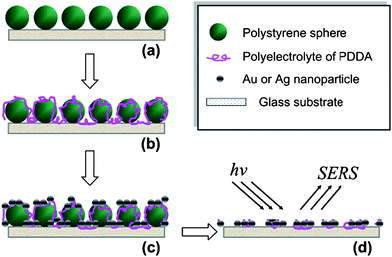 | ||
| Scheme 1 Schematic representation of deposition process by using LbL self-assembly and NSL: (a) PS spheres array on a glass substrate, (b) deposition of polyelectrolyte, (c) assembly of Au or Ag nanoparticles, and (d) nanowell array after removing PS templates. | ||
Fig. 1a shows the typical SEM image of an hpc PS monolayer, indicating that a large-area and ordered 2D monolayer consisting of PS spheres (av 600 nm) has been obtained successfully. Fig. 1b shows the SEM image of the Au nanoparticles (av 17 nm) deposited on PDDA modified glass substrates. It demonstrates that Au nanoparticles are uniform and can be deposited on PDDA film easily. This SEM image is selected to show the typical morphology of metal colloid coated polyelectrolyte film.
 | ||
| Fig. 1 SEM images of (a) 2D PS spheres (av 600 nm) array in a hexagon close-packed pattern on glass substrates, and (b) Au nanoparticles (av 17 nm) monolayer deposited on PDDA modified glass substrates. | ||
Fig. 2 shows the noble metal nanoparticles coated PS films. The polyelectrolyte of PDDA was employed as adhesive between the PS template and metal nanoparticles. A strong interaction including van der Waal attraction, capillary force (induced by the PS microarray) and electrostatic force (induced by the contrary charges of PDDA and nanoparticles) contributed to the self-assembly on the substrate surfaces. In our experiments a soaking time of 20 min was selected for PDDA. It is much longer than the saturated adsorption time of PDDA (5 min as usual). We believe that the saturated adsorbed PDDA is sufficient for successive Au/Ag attachment. Au nanoparticles (av 17 nm) coated PS film is shown in Fig. 2a. The result indicates that the monolayered PS film is a wonderful template for 2D patterns. The ordered nanoparticle islands replicated the period of PS templates exactly. Due to the versatile application of LbL self-assembly, it can also deposit other kinds of nanoparticles. Herein, Ag nanoparticles were applied as building blocks too. Fig. 2b shows the SEM image of Ag nanoparticles (av 12 nm) coated PS film. The uniform structure proved the generality of this method for construction of patterning surfaces.
 | ||
| Fig. 2 SEM images of PS spheres monolayer (av 600 nm) coated with (a) a monolayer of Au nanoparticles (av 17 nm), and (b) a monolayer of Ag nanoparticles (av 12 nm). | ||
Patterns on glass substrates were obtained by removing PS templates. It should be noted that the removal of PS spheres did not affect the self-assembled layers of Au/Ag nanoparticles on glass slides. Because the Au/Ag nanoparticles have a strong electrostatic interaction with PDDA and neither of them disperses in acetone. A periodic nanowell array has been prepared and characterized by AFM. Fig. 3a shows the typical AFM image of Au nanowell array. The ordered micro/nanostructures can be seen clearly. A line scan (Fig. 3b) was performed to determine the geometry of the film. This film has nanowells with an average diameter of about 325 nm and an average depth of 17 nm, respectively. Fig. 3c shows the line scan and side view of Ag nanowell array. The Ag film has the similar structure to Au film. The diameter and depth of the wells are approximately 337 and 12 nm, respectively.
 | ||
| Fig. 3 (a) AFM image of Au nanowell array consisting of Au nanoparticles (av 17 nm) on the glass slides. (b) The cross-sectional contour of Au nanowell array. The diameter and depth of the wells are approximately 325 and 17 nm, respectively. (c) The cross-sectional contour and side view of Ag nanowell array consisting of Ag nanoparticles (av 12 nm) on the glass slides. The diameter and depth of the wells are approximately 337 and 12 nm, respectively. | ||
By combining NSL and LbL self-assembly, we can obtain Au/Ag nanowell arrays easily as demonstrated above. This effective way provides an opportunity to produce surface modifications which have applications in SERS analysis.
Fig. 4 shows the SERS spectra of 10−4 mol L−1 4-ATP absorbed on such Au nanowell arrays at different locations. As a result, the SERS intensities were homogeneous as a whole. It is reasonable to conclude that the SERS spectra reflect the uniform dispersion of Ag nanowell arrays on the whole surface.
 | ||
| Fig. 4 SERS spectra of 10−4 mol L−1 4-ATP absorbed on Au nanowell arrays at different locations. | ||
The SERS enhancement factor (EF) can be estimated following the previously reported method.27,28 Briefly, the samples for SERS measurements were prepared by drop coating of 10 μL of 4-ATP (10−4 mol L−1) ethanol solution onto the patterning Au/Ag films, and then they were dried naturally. 10 (±0.5) mm diameter circular blots were formed on the substrates. The average surface coverage was calculated to be 7.67 × 10¹⁴ molecules cm−2. Thus, the average occupied area of one 4-ATP molecule was about 13 Å2. It was obviously less than the area occupied by a 4-ATP (about 20 Å2) assuming that 4-ATP molecules were vertically adsorbed on substrates.29 So, we can also conclude that the 4-ATP deposited film was not a monolayer. The peak at 1077 cm−1 was chosen for quantitative analysis. EF can be defined as the following:

4. Conclusions
In summary, a facile and powerful method to form Au/Ag nanowell arrays by combination of NSL and LbL self-assembly is proposed in this work. It is a unique technique for surface functionalization with periodic patterning. After the surface modification, a desired SERS activity was generated on the substrates. The EF is calculated to be 104 ∼ 105 with high homogeneity. Such an approach can easily be extended to other analytical substrates. It is an ideal method for the surface modification and SERS analysis.Acknowledgements
The authors are most grateful to the NSFC, China (Grant No. 20827004) for financial support. W. D. R. is also grateful to the Postdoctoral Science Foundation of China (Grant No. 20090451146).References
- C. Y. Huang, G. Q. Jiang and R. Advincula, Macromolecules, 2008, 41, 4661 CrossRef CAS.
- X. Zhang, F. Shi, X. Yu, H. Liu, Y. Fu, Z. Q. Wang, L. Jiang and X. Y. Li, J. Am. Chem. Soc., 2004, 126, 3064 CrossRef CAS.
- D. V. Andreeva, D. Fix, H. Mohwald and D. G. Shchukin, J. Mater. Chem., 2008, 18, 1738 RSC.
- X. Y. Wang, X. L. Xie, C. F. Cai, E. Rytting, T. Steele and T. Kissel, Macromolecules, 2008, 41, 2791 CrossRef CAS.
- M. C. Berg, L. Zhai, R. E. Cohen and M. F. Rubner, Biomacromolecules, 2006, 7, 357 CrossRef CAS.
- N. Kohli, D. Srivastava, J. Sun, R. J. Richardson, I. S. Lee and R. M. Worden, Anal. Chem., 2007, 79, 5196 CrossRef CAS.
- A. Mallardi, M. Giustini, F. Lopez, M. Dezi, G. Venturoli and G. Palazzo, J. Phys. Chem. B, 2007, 111, 3304 CrossRef CAS.
- S. L. Clark, M. F. Montague and P. T. Hammond, Macromolecules, 1997, 30, 7237 CrossRef CAS.
- S. L. Clark and P. T. Hammond, Adv. Mater., 1998, 10, 1515 CrossRef CAS.
- K. M. Chen, X. P. Jiang, L. C. Kimerling and P. T. Hammond, Langmuir, 2000, 16, 7825 CrossRef CAS.
- X. Jiang and P. T. Hammond, Langmuir, 2000, 16, 8501 CrossRef CAS.
- X. P. Jiang, S. L. Clark and P. T. Hammond, Adv. Mater., 2001, 13, 1669 CrossRef CAS.
- F. Hua, J. Shi, Y. Lvov and T. Cui, Nano Lett., 2002, 2, 1219 CrossRef CAS.
- W. D. Ruan, C. X. Wang, N. Ji, Z. C. Lu, T. L. Zhou, B. Zhao and J. R. Lombardi, Langmuir, 2008, 24, 8417 CrossRef CAS.
- A. Stein, Microporous Mesoporous Mater., 2001, 44, 227 CrossRef.
- A. Stein and R. C. Schroden, Curr. Opin. Solid State Mater. Sci., 2001, 5, 553 CrossRef CAS.
- J. C. Hulteen and R. P. Van Duyne, J. Vac. Sci. Technol., A, 1995, 13, 1553 CrossRef CAS.
- A. Stein, F. Li and N. R. Denny, Chem. Mater., 2008, 20, 649 CrossRef CAS.
- E. Vekris, V. Kitaev, D. D. Perovic, J. S. Aitchison and G. A. Ozin, Adv. Mater., 2008, 20, 1110 CrossRef CAS.
- C. L. Haynes and R. P. Van Duyne, J. Phys. Chem. B, 2001, 105, 5599 CrossRef CAS.
- K. A. Willets and R. P. Van Duyne, Annu. Rev. Phys. Chem., 2007, 58, 267 CrossRef CAS.
- M. E. Stewart, C. R. Anderton, L. B. Thompson, J. Maria, S. K. Gray, J. A. Rogers and R. G. Nuzzo, Chem. Rev., 2008, 108, 494 CrossRef CAS.
- M. A. Correa-Duarte, A. Kosiorek, W. Kandulski, M. Giersig and V. Salgueirino-Maceira, Small, 2006, 2, 220 CrossRef CAS.
- W. D. Ruan, Z. C. Lu, N. Ji, C. X. Wang, B. Zhao and J. H. Zhang, Chem. Res. Chin. Univ., 2007, 23, 712 Search PubMed.
- G. Frens, Nature Phys. Sci., 1973, 241, 20.
- J. A. Creighton, C. G. Blatchford and M. G. Albrecht, J. Chem. Soc., Faraday Trans. 2, 1979, 75, 790 RSC.
- Z. C. Lu, W. D. Ruan, J. X. Yang, W. Q. Xu, C. Zhao and B. Zhao, J. Raman Spectrosc., 2009, 40, 112 CrossRef CAS.
- J. Zhou, S. P. Xu, W. Q. Xu, B. Zhao and Y. Ozaki, J. Raman Spectrosc., 2009, 40, 31 CrossRef CAS.
- Y. L. Wang, X. Q. Zou, W. Ren, W. D. Wang and E. K. Wang, J. Phys. Chem. C, 2007, 111, 3259 CrossRef CAS.
Footnote |
| † Electronic supplementary information (ESI) available: TEM image of Ag nanoparticles with an average diameter of 12 nm. See DOI: 10.1039/c0ay00068j |
| This journal is © The Royal Society of Chemistry 2010 |