Microfluidic colourimetric chemical analysis system: Application to nitrite detection
Vincent J.
Sieben
*ab,
Cedric F. A.
Floquet
b,
Iain R. G.
Ogilvie
b,
Matthew C.
Mowlem
b and
Hywel
Morgan
a
aNanoscale systems integration group, University of Southampton, Southampton, UK SO17 1BJ. E-mail: hm@ecs.soton.ac.uk; v.sieben@noc.soton.ac.uk; Fax: +44 (0)23 8059 3029; Tel: +44 (0)23 8059 3330
bNational Oceanography Centre, University of Southampton, Southampton, UK SO14 3ZH. E-mail: mcm@noc.soton.ac.uk; Fax: +44 (0)23 8059 6149; Tel: +44 (0)23 8059 6379
First published on 19th February 2010
Abstract
The design, fabrication, analysis and characterisation of a continuous flow, microfluidic absorption cell and detection system is described. A low cost optical illumination and detection method is integrated with a simple microfluidic system. Nitrite is detected at nM concentration using the Griess reaction. The device is based on a novel optical absorption scheme with microfluidic channels made from tinted PMMA. An absorbance path length of 25 mm enables nitrite to be detected from 50 nM to 10 μM with a limit of detection of 14 nM. The system was used to characterise the reaction kinetics and maximum sample resolution. In this report the system is used to detect nitrite, but it could equally be used to assay a range of different chemistries using colourimetric methods. The system provides a cost-effective, simple system that could be deployed in a range of scenarios for environmental monitoring.
Introduction
Determination of nitrite levels in oceans, rivers and drinking water is of importance in environmental monitoring since nitrite is both a nutrient and excretion product of phytoplankton1 and is important in the global nitrogen and carbon cycles with concomitant effects on climate.2 Excessive concentrations are also dangerous to human health and aquatic organisms.3 The current guideline of maximum permissible nitrite levels in drinking water according to the World Health Organisation is 3 mg L−1 (65.2 μM) for short-term exposure and 0.2 mg L−1 (4.3 μM) for long-term exposure.4 Concentrations are typically below 0.2 μM in the ocean but can vary from 0.1–50 μM depending on location.5 Exposure to high-levels of nitrite has been shown to be detrimental to marine life for example; adversely affecting fish growth, gill osmoregulatory function, blood oxygen carrying capacity, and ionic homeostasis.6 In humans, excess nitrite can cause methaemoglobinaemia,4 as well as being an important precursor in the formation of many carcinogens.7 Elevated levels of nitrite are commonly caused by fertiliser leaching or runoff, sewage discharge and anaerobic conditions.4 As such, it has become increasingly important for industrialised countries to monitor and sample concentration levels of nitrite to safeguard human health and increase knowledge of organic life and the environment.8Although commercial systems currently exist to measure nitrite concentrations9,10 their large physical size (e.g. 440 mm long and 127 mm dia.)9 and power consumption (typically greater than 10 W) limit their deployment capabilities and scenarios. Furthermore, sample deterioration can rapidly occur due to the reactivity of nitrite; therefore, a strong motivation exists for the development of on-site measurement systems.3 Our aim is to produce an on-site nitrite sensor that is compact and low-cost to be used on small vehicles11 or buoys.12 Such a miniaturised system would permit large-scale remote monitoring of nitrite concentrations (as well as a variety of analytes, dissolved gases, nutrients, and trace metals using reagents and UV-Vis absorption)13 in a wide range of aquatic environments.
Current techniques for the detection of nitrite include: electrochemical, capillary/column, biosensing and spectrophotometry.3,10,14–16 Electrochemical amperometric techniques are inadequate for monitoring trace nitrite concentrations3 (often limited to 4 μM) and they are unstable due to fouling of the electrode surface when exposed to real samples.7 Similarly, biosensor approaches need to address operational robustness, selectivity and standardisation,3 although, recent advances have somewhat improved stability.8 Capillary/column-based approaches are considerably more robust; however, the large instrumentation and operational demands (including the need for trained personnel) hinder their potential use for automated on-site monitoring. Of the various methodologies available for nitrite detection, spectrophotometric approaches are currently more viable and economical for a miniaturised nitrite sensor.15
A variety of colourmetric assay chemistries exist; the Griess assay has been the mainstay of nitrite analysis for over a century.3,16–18 The Griess method relies on the formation of an Azo dye by the reaction of sulfanilamide hydrochloride and N-(1-Naphthyl)ethylenediamine dihydrochloride (N.E.D.) with nitrite. The optical absorption of this Azo dye (formed in the presence of nitrite) is centered at ∼543 nm (FWHM ≈ 82 nm) and is linearly proportional to the concentration of nitrite. The wide-spread adoption of this technique is due to the selectivity of the reaction, and the ability to observe the absorption wavelength window in real world environmental samples.3 Several variations and practical implementations of the Griess reaction have successfully measured nitrite concentration in a range of sample environments, including: raw seawater, grape wines, snow, soil, tap water and sewage.19,20 Each sample environment requires process optimisation, and these modifications are described in the literature.20 When the Griess method is combined with continuous flow conditions, it enables the highest possible sample throughput.16 By coupling flow injection analysis (FIA) spectrophotometry with the Griess method, the absorption of light over a segment of fluid sample can be measured and related to the concentration of nitrite. Although the Griess method is stable, sensitive and robust, typical FIA systems consume vast amounts of reagent (approx. 5–20 ml/sample)19 making the technique unsuitable for long-term, on-site and remote deployment.
Microfluidic platforms offer a solution to this reagent consumption problem, as well as the size and power challenges associated with macro-sized wet chemical sensors. Furthermore, micro-systems combine a wide-range of technologies that offer unique abilities for integrating several sub-systems to realise a completely embedded sensor system (including optics, flow control, and electronics).21–24 Due to the advantages of microfluidics (system-level integration, lowered reagent consumption, smaller sensor size, reduced power requirements, etc.), there has been an increased application of this technology in environmental monitoring.24–26
Early work in developing microfluidic platforms for colourimetric sensing was performed by Greenway et al.27 who implemented the Griess reaction on a glass microfluidic device similar to the one developed by Daykin and Haswell.28 The system utilised electro-osmotic flow (EOF) for pumping and external optical components for absorbance measurements and achieved a limit of detection (LOD) of 0.2 μM. The system was also adapted to include a cadmium reduction column for the analysis of nitrate.29 Other groups used LEDs and photodetectors for detection, further integration and cost reduction.30–32 Many of these microchip absorption cells had small path-lengths and difficulty in coupling the optical components to the chip, leading to reduced sensitivities and high LODs.33
To reduce cost, recent devices have been fabricated in poly(methylmethacrylate) (PMMA).34–36 He et al.15 developed a chemiluminescence-based microflow injection analysis system on a chip for the determination of nitrite. The chip was fabricated in PMMA, and was capable of measuring only 1.8 μL of sample. The system was based on a reaction of luminol with ferricyanide, achieving a linear detection range of 0.17–2.2 μM. They compared their sensor with the standard bench-top Griess method and the results were in agreement. Although this initial work demonstrated a μFIA system for the detection of nitrite on-chip, it employed expensive optical components, such as a PMT. Others have taken more cost-effective approaches; O'Toole et al.37 employed the Griess method for the detection of nitrite with a FIA system in conjunction with a novel Paired Emitter-Detector Diode detection method and they are working toward microfluidic realizations.25,37,38
In this work we demonstrate the use of lab-on-a-chip technologies to miniaturise the gold-standard Griess assay for detecting nitrite. In the microfluidic chip implementation of the Griess assay, we demonstrate a novel platform based on tinted PMMA, shown in Fig. 1, which integrates both the fluid processing and the optical detection, enabling the development of a low-cost, miniature, portable and sensitive environmental nitrite sensor. The chip mixes a sample with the Griess reagent to create a coloured Azo dye whose absorbance is proportional to the concentration of nitrite. In the chip there are four separate absorbance cells (2.5 cm path length) separated by three serpentine mixers. This design was implemented to monitor the kinetics of the reaction and the efficiency of mixing and dispersion within the system.
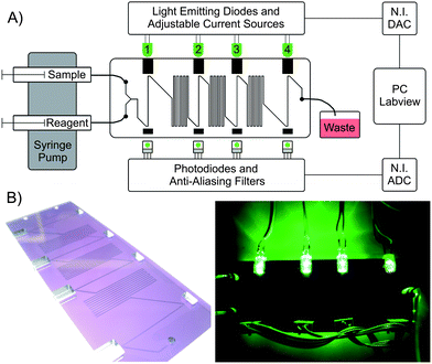 | ||
| Fig. 1 A) The schematic layout of the microfluidic setup. The Y-inlet is used to mix sample with the Griess reagent (both driven by syringe pump) to detect nitrite concentrations via the formation of Azo dye, which appears pink when developed. After combining the reagents, there are four dog-legged absorbance detection cells (25 mm long) separated by three serpentine mixers. Microchannels are 300 μm wide and deep in PMMA, and each serpentine is 250 mm long (total chip channel length of 998 mm). A personal computer running Labview was used to control a National Instruments data acquisition card, which adjusted LED intensity and measured the degree of absorbance from the photodiodes. B) Photographs of the microfluidic device (95 mm long, 37 mm wide and 6 mm thick) with integrated optical components (the left photo was taken on a light table so that microchannels were visible in tinted-PMMA). Grooves were milled into the tinted PMMA to hold and align the LEDs and photodiodes. | ||
Experimental
Microfluidic chip fabrication
The microfluidic chip shown in Fig. 1 was made from tinted PMMA created by micro-milling (LPKF Protomat S100 micromill) and solvent vapour bonding procedure.39 The lid and microfluidic chip were machined with alignment features and solvent bonded in a hot-press (LPKF laser and electronics AG, Garbsen, Germany). The channels were 300 μm wide and deep machined into 3.0 mm thick tinted PMMA polymer sheet (Plexiglas GS 7F60, Röhm, Darmstadt, Germany). Fluidic connectors were milled into the lid and grooves were machined to accommodate the LEDs and photodiodes for self-alignment. After fabricating the chip, the optical components were fixed with Norland optical adhesive 68 (NJ, USA), please see Fig. 1.Chemistry
The most common coupling reagent for the Griess reaction is N.E.D. and it has several advantages over other reagents; reproducibility, speed of reaction, sensitivity, acid-solubility of Azo dye and pH independence of the colour in the pH range of 1–2.40 In fact, the use of N.E.D. and sulfanilamide has been established as a European standard method of determining nitrite concentrations in drinking water (BS EN ISO13395). The reagent used for the detection of nitrite in this paper was based on Tovar et al.5 The “Griess reagent” was created by dissolving 0.5 g of sulfanilamide (CAS-No: 63-74-1, EC-No: 200-563-4, Fisher Scientific, UK), in approx. 50 mL of MilliQ water and 5 mL of concentrated hydrochloric acid (Sigma-Aldrich, UK) in a 500 mL volumetric flask. Once dissolved, 0.05 g of N.E.D. (CAS-No: 1465-25-4, EC-No: 215-981-2, Sigma-Aldrich, UK) was added and MilliQ water was added to make a total volume of 500 mL. The hydrochloric acid created the acidic conditions (pH 1–2) under which nitrite reacts with sulfanilamide. Standard nitrite solutions were created by dissolving 6.9 g of sodium nitrite (NaNO2, CAS-No: 7632-0-0, Fisher Scientific, UK), into 1 L of MilliQ water. This 100 mM stock solution was then diluted with MilliQ water to create the various concentrations used in this study to validate the on-chip optical absorption cell. The Griess reagent and the nitrite standard were pumped through the separate inlets at a flow rate of 50 μL min−1 (total flow rate of 100 μL min−1) with syringe pumps (Harvard Apparatus Nanomite, Kent, UK) driving two 500 μL Hamilton 1750CX syringes (Nevada, USA).Optical cell
A schematic diagram of the machined optical absorbance cell is shown in Fig. 2. It has 1 mm thick windows separating the LED or photodetector from a 25 mm long absorbance cell. A LED was used as the light source to facilitate miniaturisation and integration, reduce power consumption, lower system cost, and enhance robustness.41 The LED used was a HLMP-CM14-Z30DD from Avago technologies (CA, USA), which has a luminous efficiency of 56 lm/W (greater than 4 times that of an incandescent lamp (13 lm/W).41 The dominant wavelength is 525 nm; Fig. 3 shows a measured emission spectrum (Ocean Optics HR4000CG-UV-VIS-NIR spectrophotometer, FL, USA).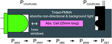 | ||
| Fig. 2 Cross-sectional view of the microfluidic absorption cell with optical power budget (see text for details). PMAX is the maximum power that will reach the detector from the LED (determined by the solid angle), PCOUPLING is the power remaining after the lumped losses from coupling the LED and photodetector to the microfluidic device, PWIN1 is the power remaining after the first window, PABS is the power remaining after the adsorption of the Azo dye formed in the presence of nitrite (desired measurement), PWIN2 is the power remaining after the detection window and PDET is the optical power that is detected. | ||
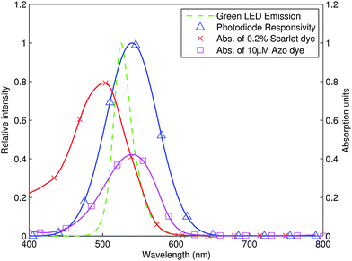 | ||
| Fig. 3 Measured absorption spectra of 10 μM Azo dye and 0.2% scarlet food dye in a 10 mm detection cell. The measured emission spectrum of the Avago green LED and approximate photodiode spectral responsivity are also shown. | ||
The optical power budget and light collection efficiency of this setup can be estimated as follows. The LED emits light into a 15° cone, but only a fraction reaches the detector. There is also loss due to the misalignment of the LED and photodiode against the tinted PMMA windows and absorption of light by the material in the windows. To estimate the maximum optical power that reaches the photodiode we determine the solid angle subtended by the collection path from eqn (1), assuming an isotropic beam profile within the 15° cone.
| PMAX = Ie ΩDet = (ILED/ηv)(HW/L2) | (Eqn 1) |
P MAX is the maximum power that reaches the detector (assuming the detector is larger than the exit window and that there is no background light), Ie is the radiant intensity, Ie = ILED/ηv, where ILED is the minimum luminous intensity in candelas (12cd minimum for the LED), and ηv is the luminous efficacy in lumens/watt (545 lm/W for the LED), ΩDet is the detection solid angle, estimated as the channel cross-sectional area (HW, 300 μm × 300 μm) over the length of the optical path squared (L, 27 mm). The maximum calculated optical power that reaches the detector is approximately 2.7 μW, yielding a light collection efficiency of 0.23% (Pmax divided by total power over 15° cone).
Geometrical mismatch, scattering by surface roughness on the channel walls, angular dependence of illumination and detection, intensity variations of LED emission and photodiode detection etc. all contribute to reducing the optical efficiency. These losses can be lumped together as PCOUPLING, Fig. 2. Each complete micro-fabricated system has therefore different values of losses. Experimentally these losses are of the order of ×5, meaning that only 20% of the incident light is transmitted; consistent with the literature.42 The remaining optical power is approximately 544 nW.
The light crosses two tinted PMMA windows and the power loss at these windows was estimated from absorbance measurements made of the PMMA. The loss through each 1 mm window was calculated to be 51.5% (48.5% transmitted); meaning that 128 nW of power is available for the absorption cell.
The concentration of a molecule in a solution is related to photon absorption by the Beer–Lambert law:41
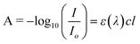 | (Eqn 2) |
The light is converted to a voltage signal with a photodiode (TSLG257-LF, TAOS - Texas Advanced Optoelectronic Solutions Inc., TX, USA), band-width of approximately 2.2 kHz, with an integrated green optical filter. Fig. 3 shows the relative responsivity spectrum.41 The output voltage is proportional to light intensity according to
| V = ReIDET | (Eqn 3) |
The data was collected using a National Instruments Digital Acquisition Device PCI 6289 card with a sampling rate of 110 Hz and an anti-aliasing filter set at 1.6 Hz. The signal was further filtered using a software low-pass filter to remove any components above 2 Hz. Data shown in the figures was processed with a lowpass Butterworth filter implemented in software with n = 1, w = 0.0005.
Results and discussion
Calibration
The microchip was calibrated using scarlet food dye and nitrite standards, and the results compared with a Hitachi U-2800 dual beam spectrophotometer. For the calibration studies, a single syringe was used to pump the sample into the chip via the waste with both inlets set to waste. Syringes were filled with sample (blank, dye, or nitrite) and the reagent was delivered to the microchip at a flow rate of 100 μL min−1.Fig. 4(a) shows the output voltage for each of the four photo-detectors for different concentration of scarlet food dye (0.002% to 0.4% v/v). MilliQ blank samples were injected into chip for 5 min, followed by the dye samples for 5 min. This was repeated for each dye concentration. The blank baseline drift was typically less than 20 mV over 100 min for all experiments. This data was imported into MATLAB and a curve fitting script used to discriminate sample from the blanks by detecting a change in gradient, and to the calculate absorption by averaging the signal (voltage) over a 45 s window in the center of each sample. This voltage was converted into absorption from the ratio of this voltage to preceding blank voltage. The absorbance values for the Scarlet dye samples are shown in Fig. 4 (b).
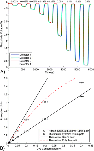 | ||
| Fig. 4 A) The photodiode output voltage for all four detectors for a sequence of scarlet dye samples of varying concentrations, 0.002% to 0.4% v/v, passing through the microfluidic device. MilliQ blank sample was injected for 5 min, followed by dye sample for 5 min. This was repeated for the range of dye concentrations shown. The blank baseline drift was less than 20 mV over 100 min. The flow rate was 100 μL min−1. B) The absorbance of the scarlet dye samples shown in (A), plotted versus concentration. The dye samples were run on the microchip, as well as a Hitachi U-2800 dual-beam spectrophotometer. The theoretical Beer's law curves were determined by calculating the ε from the 0.2% sample at 525 nm and plotted using eqn (2) for the concentration range shown and for two path lengths; 10 mm (spectrophotometer) and 25 mm (chip). The theoretical polychromatic line was determined from the spectra, shown in Fig. 3, to predict the absorbance versus concentration when taking into account 1) the polychromatic light source, 2) the wavelength dependent terms in the absorption cell, 3) the spectral sensitivity of the photodiode, and 4) the variation in ε of the dye versus wavelength. Experimental results were in agreement with this prediction. | ||
The same samples were also measured using a Hitachi U-2800 dual-beam spectrophotometer, also shown in Fig. 4(b). The extinction coefficient was determined from the absorption measurement of the 0.2% sample (at 525 nm) using the spectrophotometer. This was then used to calculate the theoretical absorption curve (Fig. 4(b)) for the two path lengths of 10mm (spectrophotometer) and 25 mm (chip). The theoretical polychromatic absorption curve was determined from the spectra shown in Fig. 3. This curve predicts the absorbance vs. concentration plot as a function of wavelength, and takes into account 1) the polychromatic light source, 2) the wavelength-dependent terms in the absorption cell, 3) the spectral sensitivity of the photodiode, and 4) the wavelength dependence of the extinction coefficient of the dye. The experimental results are in agreement with this prediction as shown by Fig. 4(b), dashed line.
Next, samples with varying nitrite concentration were pumped through the chip. Fig. 5 (A) shows the same data as for the dye with nitrite concentrations ranging from 50 nM to 50 μM. The odd spike in the data is due to air bubbles in the system. The 50 μM sample (equivalent to 5 absorption units for this chip path length), shows the maximum DC offset (approximately 40 mV) which comes from ambient and stray background light. The absorbance of the nitrite samples plotted versus concentration is shown in Fig. 5 (B). The theoretical absorption curves were calculated using literature values of the extinction coefficient (for the two path lengths). ε was also determined using the Hitachi U-2800 spectrophotometer, giving a value of 3.9 × 10⁴ M−1 cm−1 at 525 nm, compared with a literature value of ≈ 4.0 × 10⁴ M−1 cm−1 at 520 nm.19,20,44
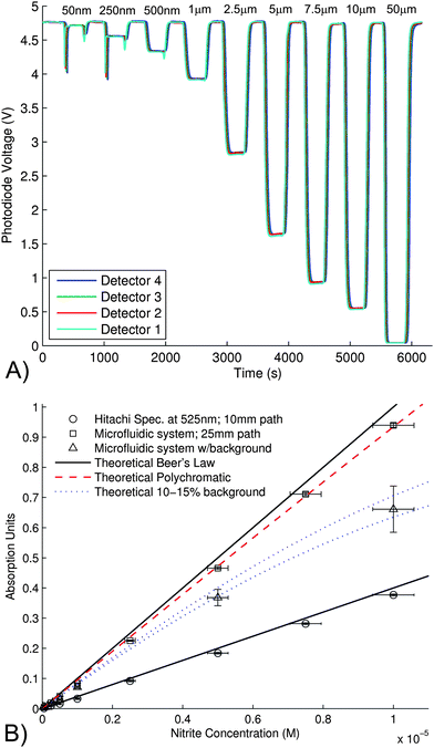 | ||
| Fig. 5 A) The photodiode output voltage for all four detectors for a sequence of nitrite samples of varying concentrations from 50 nM to 50 μM, flowing through the microfluidic device. MilliQ blank sample was injected for 5 min, followed by nitrite sample for 5 min. This was repeated for the range of nitrite concentrations. The flow rate was 100 μL min−1. The spikes at the transitions were air bubbles that entered the system when switching from blank to sample. The 50 μM sample (equivalent 5 Absorption Units for the chip path length), was used to evaluate the background noise in the system (approximately 40 mV). B) The absorbance of the nitrite samples shown in (A), plotted versus concentration (squares). The theoretical Beer's law curves (solid lines) were determined from the literature for the two path lengths of 10 mm (spectrophotometer) and 25 mm (chip). The theoretical polychromatic curve (dashed) was determined by taking into account the wavelength dependence of the optical source, cell and detector. This graph also shows the influence of background light. The theoretical background curve (dotted) shows the expected outcome (validated by the data on the graph, triangles), when 10–15% background light intensity was added to the system; demonstrating the need to minimise ambient light sources (external to the detection path). | ||
The theoretical polychromatic line was determined from the spectra shown in Fig. 3 similar to the dye but also including the wavelength dependence of ε for the Azo dye. The experiment results are in agreement with this prediction – Fig. 5(b). To accurately model the microchip, the effect of the stray light must also be included in the calculation. Fig. 5(b) shows the results including either 10 or 15% stray light together with modelled polychromatic response. Also shown is the experimental data which lies midpoint between these limits. The small amount of stray light leaking into the photodetector was eliminated by completely isolating the illumination source from the detector using black thermoplastic glue. The data for this chip is also shown, together with the polychromatic prediction (no background correction) from the Beer–Lambert law.
A comparison between this version of the microchip and the Hitachi U-2800 spectrophotometer shows excellent linear correlation with slope equal to the ratios of path lengths. However, the data for the dye cannot be compared in this way because the absorption of the dye is not linear, and the absorption is not spectrally matched to the excitation source (Fig. 3). The deviation from linearity of absorption vs. concentration for polychromatic light is well understood;43 here we demonstrate that with careful spectral matching of the light source, dye and detector wavelength sensitivity, a simple low-cost system has similar performance to a commercial spectrophotometer. This is in contrast to previous work where additional spectral filters were required to optimize the system.41
Reaction kinetics
The Griess reaction is a two-step chemical process with two rate constants; however, the reaction can be approximated with a single rate constant.20,40 In order to optimize future microfluidic systems, the reaction kinetics were studied using our device. The kinetics of the Azo dye formation was followed by mixing 2 μM nitrite solution with Griess reagent on-chip and observing the output of the four detection cells at various flow rates at room temperature (21–24 °C) as a function of time. The mixing ratio was 1![[thin space (1/6-em)]](https://www.rsc.org/images/entities/char_2009.gif) :1; yielding 1 μM Azo dye. The results shown in Fig. 6 are for flow rates of 100 μL min−1, 50 μL min−1 and no flow. After combining reagent and sample at the Y-junction, the detectors are located downstream: detector 1–18.5 mm, detector 2–329.6 mm downstream, detector 3–638.0 mm, and detector 4–949.0 mm. Also plotted in the figure is the value of the photodiode voltage for a pre-mixed nitrite standard (1 μM), which is time invariant. At a flow rate of 100 μL min−1, the figure indicates that reaction has reached 51% completion at detector 2 (18 s.), 63% completion at detector 3 (34 s.), and 71% completion at detector 4 (51 s.), calculated from the equivalent absorption values. For a flow rate of 50 μL min−1, the reaction reached 66% completion at detector 2 (35 s.), 74% completion at detector 3 (69 s.), and 81% completion at detector 4 (102 s.). Fig. 6(b) shows the absorption values (calculated from these voltage values) normalized to a completely mixed and developed solution as a function of time. From these data, an approximate time constant for the system can be determined, as shown in Fig. 6 (B). This data includes both the effects of the reaction kinetics and the characteristics of mixing and shows that the time to reach 90% completion is 144 s, similar to stop-flow kinetic studies of the Griess reaction that require 60–430 s for 90% colour development.40,45 Note that all the times are determined for mean fluid velocities. The reaction time could be decreased by increasing the concentration of N.E.D, but this would lead to higher noise on the reagent blanks.45
:1; yielding 1 μM Azo dye. The results shown in Fig. 6 are for flow rates of 100 μL min−1, 50 μL min−1 and no flow. After combining reagent and sample at the Y-junction, the detectors are located downstream: detector 1–18.5 mm, detector 2–329.6 mm downstream, detector 3–638.0 mm, and detector 4–949.0 mm. Also plotted in the figure is the value of the photodiode voltage for a pre-mixed nitrite standard (1 μM), which is time invariant. At a flow rate of 100 μL min−1, the figure indicates that reaction has reached 51% completion at detector 2 (18 s.), 63% completion at detector 3 (34 s.), and 71% completion at detector 4 (51 s.), calculated from the equivalent absorption values. For a flow rate of 50 μL min−1, the reaction reached 66% completion at detector 2 (35 s.), 74% completion at detector 3 (69 s.), and 81% completion at detector 4 (102 s.). Fig. 6(b) shows the absorption values (calculated from these voltage values) normalized to a completely mixed and developed solution as a function of time. From these data, an approximate time constant for the system can be determined, as shown in Fig. 6 (B). This data includes both the effects of the reaction kinetics and the characteristics of mixing and shows that the time to reach 90% completion is 144 s, similar to stop-flow kinetic studies of the Griess reaction that require 60–430 s for 90% colour development.40,45 Note that all the times are determined for mean fluid velocities. The reaction time could be decreased by increasing the concentration of N.E.D, but this would lead to higher noise on the reagent blanks.45
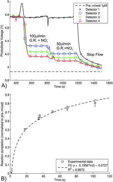 | ||
| Fig. 6 A) The development of the Azo dye along the channel for 2 μM of nitrite mixed with Greiss reagent and measured by the four detection cells (mixing ratio of 1:1; effectively yielding 1 μM Azo dye). The results shown are for flow rates of 100 μL min−1, 50 μL min−1 and stop flow. The absorption of a pre-mixed nitrite standard (from previous data) was included in the figure to indicate the degree to which the reaction reaches completion (please see text for further details). The first detector shows signs of the Schlieren effect. Markers are used to differentiate the channels and does not indicate sampling rate. For the first 400 s of the experiment, milliQ sample was flushed through the chip. B) The absorption values, calculated from the voltages in A), normalized to a completely mixed and developed solution as a function of time. Error bars indicate the standard deviation for three experiments (n = 3). | ||
System resolution
For remote deployment, the system should be able to resolve changing nitrite concentrations with high temporal resolution. To determine this figure, the system was first flushed with MilliQ water, then a sample of dye (0.025% Scarlett dye) was passed through the system at a flow rate of 100 μL min−1, and the outputs of the detectors monitored. The data is shown in Fig. 7(A) and illustrates the effect of Taylor dispersion in the system. At this flow rate, the average transition time for the sample concentration to change from 10% to 90% of the steady-state value is 53.6 ± 2.1 s (e.g. dotted line for det. 1 on graph). A similar experiment for pre-mixed nitrite (Azo dye) at 5μM concentration showed a transition time of 47.9 ± 2.4 s at a flow rate of 100 μL min−1. For the specific microchannel dimensions, this corresponds to a path length of 888 mm or a volume of 80 μL (approximately the total volume of the chip). Therefore, the maximum sampling resolution of this system is approximately 1 sample per minute. The figure shows that the gradient of the change is the same for all four detectors, which means that at this flow rate, the effect of Taylor dispersion is minimal.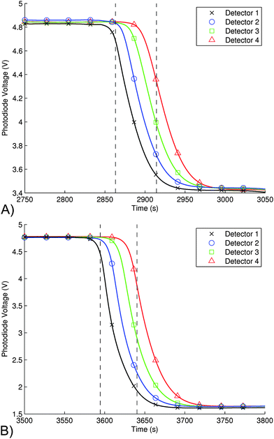 | ||
| Fig. 7 A) The transition from a blank sample to 0.025% Scarlett dye (t = 2750–3050 s. from Fig. 4A); used to determine the time required to exchange samples in the microchip absorbance cells as measured by all four detectors; i.e. the Taylor dispersion present in the system. As shown, the average transition time from 10% to 90% (shown for det. 1 on the graph) of the steady-state value is 53.6 ± 2.1 s at a flow rate of 100 μL min−1. B) Transition from blank to 5 μM pre-mixed nitrite (Azo dye) sample (t = 3500–3800 s. from Fig. 5A). The time required was 47.9 ± 2.4 s at a flow rate of 100 µL min−1. With our microchannel dimensions, this corresponds to 888 mm or 80 μL (approximately the volume of the chip). Therefore, the maximum sampling resolution of this system is approximately 1 sample per minute. | ||
Limit of detection
The limit of detection (LOD) and sensitivity is determined by noise level within the system. Noise arises from electrical interference (radio frequency, mains), circuitry noise (Johnson, amplifier and flicker), chemical noise and pH changes, flow rate fluctuations, and bubbles or debris. From our observations, fluctuations in flow rate and bubbles/debris dominate the noise within the system. For the nitrite experiment (Fig. 5) the average standard deviation of the blank samples (three runs, four detectors, eight blanks excluding the 50 μM baseline, n = 96) is 4.8 mV ± 0.8 mV (maximum value of 9.1 mV). Similarly, the average standard deviation for the nitrite samples (n = 96) is 3.2 mV ± 0.8 mV (maximum value of 7.2 mV). Using the conventional definition for the LOD (three times the blank baseline noise) gives a value of ≈15 mV for the absorption cell, which corresponds to 1.4 milli-absorption Units. This means that the LOD of nitrite is 14 nM (with a baseline of 4.75 V, just below photodiode saturation). From a practical perspective, the maximum standard deviation of all data points (15.4 mV) is a more useful measure, which equates to 4.1 milli-absorption Units or 41 nM of nitrite. This figure is similar to other spectrophotometric assays, for example, Melchert et al.46 developed a flow injection technique that had a LOD of 174 nM for a 10 mm path length cell. Typical levels of nitrite in drinking water are in the low μM range, but aquatic environment are typically 200 nM and can be as low as 100 nM.5 The system described in this work has a LOD of 14 nM and is therefore ideally suited to continuous measurement of nitrite in a range of environments. Further improvements could be made by using a longer flow cell, but this reduces temporal resolution and the dynamic range. A differential measurement system with lock-in amplifiers would further reduce sources of noise and improve the LOD.41Conclusions
We have demonstrated a novel and generic low-cost, high performance colourimetric detector based on a tinted PMMA absorbance cell. The optical design described was applied to a system for detecting nitrite in a microfluidic device. The system had integrated LEDs and photodiodes and achieved a LOD of 14 nM and a linear range between 50 nM and 10 μM. The low-power (480 mW) and low-cost microfluidic system could be further developed to include on-chip valves and pumps, which will reduce dead volume and significantly improve temporal resolution (subject to reaction kinetics). A fully integrated and miniaturized system could be deployed remotely to continuously measure nitrite concentrations in the environment. In particular a small low cost device could be used to profile the temporal and spatial distribution of chemistry in the oceans, something that is not possible with current methods.Acknowledgements
The authors acknowledge funding from ESPRC, NERC and also the University of Southampton. V. Sieben is supported in part by the Natural Sciences and Engineering Research Council of Canada. The authors would also like to thank Alan Taberham for his preliminary work on this project. We would also like to acknowledge the excellent technical support provided by Lee Fowler and Rob Brown.References
- M. W. Lomas and F. Lipschultz, Limnol. Oceanogr., 2006, 51, 2453–2467 CAS.
- J. L. Sarmiento and C. LeQuere, Science, 1996, 274, 1346–1350 CrossRef CAS.
- J. Dutt and J. Davis, J. Environ. Monit., 2002, 4, 465–471 RSC.
- WHO, Guidelines for drinking-water quality, 3rd Edition., World Health Organization, Geneva, Switzerland, 2008 Search PubMed.
- A. Tovar, C. Moreno, M. P. Manuel-Vez and M. Garcia-Vargas, Anal. Chim. Acta, 2002, 469, 235–242 CrossRef CAS.
- E. E. Deane and N. Y. S. Woo, Aquat. Toxicol., 2007, 82, 85–93 CrossRef CAS.
- Z. H. Dai, H. Y. Bai, M. Hong, Y. Y. Zhu, J. C. Bao and J. Shen, Biosens. Bioelectron., 2008, 23, 1869–1873 CrossRef CAS.
- A. Zazoua, M. Hnaien, S. Cosnier, N. Jaffrezic-Renault and R. Kherrat, Mater. Sci. Eng., C, 2009, 29, 1919–1922 CrossRef CAS.
- K. S. Johnson and L. J. Coletti, Deep-Sea Res., Part I, 2002, 49, 1291–1305 CrossRef CAS.
- A. K. Hanson, Abstr. Pap. Am. Chem. Soc., 2005, 229, U152–U153.
- C. C. Eriksen, T. J. Osse, R. D. Light, T. Wen, T. W. Lehman, P. L. Sabin, J. W. Ballard and A. M. Chiodi, IEEE Journal of Oceanic Engineering, 2001, 26, 424–436 Search PubMed.
- R. E. Davis, J. T. Sherman and J. Dufour, J. Atmos. Oceanic Technol., 2001, 18, 982–993 Search PubMed.
- T. S. Moore, K. M. Mullaugh, R. R. Holyoke, A. N. S. Madison, M. Yucel and G. W. Luther, Annu. Rev. Mar. Sci., 2009, 1, 91–115 Search PubMed.
- M. Finch, D. J. Hydes and C. H. Clayson, Anal. Chim. Acta, 1998, 377, 167–177 CrossRef CAS.
- D. Y. He, Z. J. Zhang, Y. Huang and Y. F. Hu, Food Chem., 2007, 101, 667–672 CrossRef CAS.
- M. J. Moorcroft, J. Davis and R. G. Compton, Talanta, 2001, 54, 785–803 CrossRef CAS.
- J. P. Griess, Ber. Dtsch. Chem. Ges., 1879, 12, 426 CrossRef.
- A. W. Morris and J. P. Riley, Anal. Chim. Acta, 1963, 29, 272 CrossRef CAS.
- M. D. Patey, M. J. A. Rijkenberg, P. J. Statham, M. C. Stinchcombe, E. P. Achterberg and M. Mowlem, TrAC, Trends Anal. Chem., 2008, 27, 169–182 CrossRef CAS.
- V. M. Ivanov, J. Anal. Chem., 2004, 59, 1002–1005 CrossRef CAS.
- M. Behnam, G. V. Kaigala, M. Khorasani, P. Marshall, C. J. Backhouse and D. G. Elliott, Lab Chip, 2008, 8, 1524–1529 RSC.
- A. Manz, N. Graber and H. M. Widmer, Sens. Actuators, B, 1990, 1, 244–248 CrossRef.
- P. S. Dittrich, K. Tachikawa and A. Manz, Anal. Chem., 2006, 78, 3887–3907 CrossRef CAS.
- J. West, M. Becker, S. Tombrink and A. Manz, Anal. Chem., 2008, 80, 4403–4419 CrossRef CAS.
- S. Ramirez-Garcia, M. Baeza, M. O'Toole, Y. Z. Wu, J. Lalor, G. G. Wallace and D. Diamond, Talanta, 2008, 77, 463–467 CrossRef CAS.
- L. Marle and G. M. Greenway, TrAC, Trends Anal. Chem., 2005, 24, 795–802 CrossRef CAS.
- G. M. Greenway, S. J. Haswell and P. H. Petsul, Anal. Chim. Acta, 1999, 387, 1–10 CrossRef CAS.
- R. N. C. Daykin and S. J. Haswell, Anal. Chim. Acta, 1995, 313, 155–159 CrossRef CAS.
- P. H. Petsul, G. M. Greenway and S. J. Haswell, Anal. Chim. Acta, 2001, 428, 155–161 CrossRef CAS.
- M. D. M. Baeza, N. Ibanez-Garcia, J. Baucells, J. Bartroli and J. Alonso, Analyst, 2006, 131, 1109–1115 RSC.
- A. Rainelli, R. Stratz, K. Schweizer and P. C. Hauser, Talanta, 2003, 61, 659–665 CrossRef CAS.
- M. O’Toole and D. Diamond, Sensors, 2008, 8, 2453–2479.
- A. Gáspár, I. Bacsi, E. F. Garcia, M. Braun and F. A. Gomez, Anal. Bioanal. Chem., 2009, 395, 473–478 CrossRef CAS.
- E. Rodrigues and R. A. S. Lapa, Microchim. Acta, 2009, 166, 189–195 CrossRef CAS.
- S. Kruanetr, S. Liawruangrath and N. Youngvises, Talanta, 2007, 73, 46–53 CrossRef CAS.
- C. H. Wu and J. Ruzicka, Analyst, 2001, 126, 1947–1952 RSC.
- M. O'Toole, R. Shepherd, K. T. Lau and D. Diamond, in Conference on Advanced Environmental, Chemical, and Biological Sensing Technologies V, ed. T. VoDinh, R. A. Lieberman and G. Gauglitz, Spie-Int Soc Optical Engineering, Boston, MA, 2007, pp. P7550–P7550 Search PubMed.
- K. T. Lau, S. Baldwin, M. O'Toole, R. Shepherd, W. J. Yerazunis, S. Izuo, S. Ueyama and D. Diamond, Anal. Chim. Acta, 2006, 557, 111–116 CrossRef CAS.
- C. W. Tsao and D. L. DeVoe, Microfluid. Nanofluid., 2009, 6, 1–16 CrossRef CAS.
- J. B. Fox, Anal. Chem., 1979, 51, 1493–1502 CrossRef CAS.
- W. Gong, M. Mowlem, M. Kraft and H. Morgan, IEEE Sens. J., 2009, 9, 862–869 CrossRef CAS.
- C. L. Bliss, J. N. McMullin and C. J. Backhouse, Lab Chip, 2007, 7, 1280–1287 RSC.
- C. Galli, J. Pharm. Biomed. Anal., 2001, 25, 803–809 CrossRef CAS.
- A. C. Bratton, E. K. Marshall, Jr., D. Babbitt and A. R. Hendrickson, J. Biol. Chem., 1939, 128, 537–550 CAS.
- S. C. Pai, C. C. Yang and J. P. Riley, Anal. Chim. Acta, 1990, 232, 345–349 CrossRef CAS.
- W. R. Melchert, C. M. C. Infante and F. R. P. Rocha, Microchem. J., 2007, 85, 209–213 CrossRef CAS.
| This journal is © The Royal Society of Chemistry 2010 |