Ordering domains of spin cast blends of conjugated and dielectric polymers on surfaces patterned by soft- and photo-lithography
Justyna
Jaczewska
a,
Andrzej
Budkowski
*a,
Andrzej
Bernasik
b,
Ioannis
Raptis
c,
Ellen
Moons
d,
Dimitrios
Goustouridis
c,
Jakub
Haberko
b and
Jakub
Rysz
a
aM. Smoluchowski Insitute of Physics, Jagiellonian University, Reymonta 4, Kraków 30–059, Poland. E-mail: ufbudkow@cyf-kr.edu.pl
bFaculty of Physics and Applied Computer Science, AGH-University of Science and Technology, Al. Mickiewicza 30, Kraków 30–059, Poland
cInstitute of Microelectronics, NCSR “Demokritos”, Aghia Paraskevi, Athens 15310, Greece
dDepartment of Physics and Electrical Engineering, Karlstad University, Karlstad 651 88, Sweden
First published on 20th October 2008
Abstract
Spin casting polymer blends of conjugated and dielectric macromolecules onto chemically patterned metal and oxidized silicon surfaces might provide a simple method to fabricate polymer-based circuitries that can be integrated with conventional electronics. Such solution-processing of the blend components offers simultaneous deposition and pattern-directed alignment of the phase separated polymer domains. The alignment is driven by self-organization guided by preferential surface segregation. Here we demonstrate that the laterally arranged domain structures in spin cast films of the conjugated poly(3-alkylthiophenes) (P3ATs): P3BT, P3DDT and regioregular R-P3HT, blended with dielectric polystyrene (PS), can be ordered by three different surface templates. The templates are formed by a patterned self-assembled monolayer (SAM), micro-contact printed on the surface of interest, i.e. hexadecanethiols on gold (for alignment of P3DDT/PS blend) and octadecyltrichlorosilanes on oxidized silicon (for R-P3HT/PS). Additionally gold lines are micro-patterned on SiO2 with photo-lithography (for P3BT/PS mixture). The forces driving pattern-directed self-organization of the polymers are discussed based on complementary studies of preferential surface segregation, observed for blend films spin cast on homogeneous surfaces that correspond to the different regions of the surface templates.
I. Introduction
The past decade has witnessed a rapid progress in electronics based on conjugated polymers deposited on various substrates:1,2 innovative low-cost methods have been proposed to fabricate prototypes of lasers,3–5 light-emitting diodes (LEDs),6 solar cells7 and field-effect transistors (FET).8–10Spin-coating,11 as the first polymer deposition technique, has been successfully implemented on the production lines of plastic electronics.2 Deposition and patterning techniques compatible with large area surfaces and flexible substrates will be increasingly important as the technology is scaled up.To produce polymer-based circuitries for electronic devices the deposition of polymers must be controlled spatially (at least) on a micrometre-scale.12–14 This can be achieved with area-selected electro-polymerization,14,15 photochemical patterning14,16 and non-reactive methodologies.12,14 Only the latter, using dissolved pre-formed polymers, seems to be simple and versatile enough to allow mass production.2,12a Mainstream strategies following this approach are based on additive (“top-down”) polymer deposition (e.g. with screen,17 inkjet8 and micro-contact18 printing) to fabricate step-by-step all the components of the prototype devices.
Spin-coating of the dissolved polymer blends is technologically more attractive than successive polymer printing procedures: it offers a one-step deposition process in which phase domains rich in different blend components are formed and self-organize spontaneously, constituting the various device elements.19–23 An effective combination of the non-reactive patterning and blend spin casting might enable further cost reduction of plastic electronics. Böltau et al.24 have demonstrated that the phase separated domains of spin cast blends of model (dielectric) polymers can be guided by preferential segregation to a chemically pre-patterned substrate. This is the result of a rapid and complex process sensitive to many parameters:11,25–27 patterns can be transposed from the substrates into the polymer films for judiciously chosen systems, defined by the polymer mixture, the solvent and the patterned surface.24,28–31 Pattern-directed film structures depend on the length-scale commensurability between the blend and the pattern24,32,33 as well as on the match between blend composition and patterned area fraction.33,34 The patterns replicated by film morphology can be optimized by changing the spin-coating conditions.33
Recently the studies on the spin cast blends, aligned by substrate patterns, have been extended to mixtures of conjugated polymers: micro-contact printed35 patterns of self-assembled monolayers (SAMs) order the laterally arranged domains of two blends: poly(9,9′-dioctylfluorene) (PFO) mixed with a PFO-based copolymer,36 as well as (conducting) polyaniline doped with camphorsulfonic acid and blended with (dielectric) polystyrene (PS).37a A similar approach, supplemented by solvent annealing, was successfully applied to film blends of two semiconductors: poly(3-hexylthiophene) (P3HT) and (6,6)-phenyl-C61-butyric acid methyl ester.37b In turn, SAM templates, generated locally with dip-pen nanolithography38a,b or macroscopically with digital lithography,38c induce laterally controlled vertical phase structures of spin cast PS mixtures with P3HT, and poly(methyl methacrylate) blends with poly[5,5′-bis(3-dodecyl-2-thienyl)-2,2′-bithiophene)], respectively.
In this paper, we demonstrate that the chemical micro-patterns (Au/SAM, SiOx/SAM, SiO2/Au) prepared with common techniques (micro-contact printing, photo-lithography) over broad areas of silicon wafers, covered with oxidized silicon layer (native SiOx, thermally grown SiO2) or gold, can order the laterally arranged domains of spin cast conjugated poly(3-alkylthiophenes) (P3ATs: P3BT, P3DDT and regioregular R-P3HT) blended with dielectric PS.
For the three blends presented here we also discuss the forces driving the pattern-induced self-organization with the preferential surface segregation concluded from morphological analysis of P3AT/PS mixtures cast on homogeneous surfaces (Au, SiOx, SAM).
II. Results and discussion
P3AT polymers were chosen for this study, as they are a heavily studied conjugated polymer family, often used as semiconductors in various electronic devices.39–41 This is because of their high charge mobility,40,42 good solubility43 and commercial availability.42Spin casting P3AT-based macromolecules blended with insulating polymers simplifies the fabrication of such devices.44–46 This work concerns three different P3ATs mixed with dielectric PS. The mechanisms of film structure formation and the effects of the solvent, used to spin cast the P3AT/PS films onto SiOx, were studied earlier:47 lamellar (LS, LT) and lateral (quasi-2-dimensional: 2S, 2T) film structures with elevated domains rich in P3AT (superscript T) and PS (superscript S) were observed.47bSolvent exchange could induce a transition from a lamellar to a lateral domain arrangement.23,47,48 In addition, humidity-related structural modifications can be prevented if the solvents used are less hygroscopic than tetrahydrofuran.47 Here we focus on establishing pattern-guided alignment of the lateral structures of these P3AT/PS blends.All P3AT/PS films are characterized with microscopy techniques, such as atomic (AFM) and lateral (LFM) force microscopy as well as fluorescent microscopy (FM), complemented by compositional data provided by dynamic secondary ion mass spectrometry (dSIMS).49
A. P3DDT/PS blends ordered by gold micro-printed with thiols
In the first set of experiments, P3DDT/PS blends were deposited from chloroform solutions onto a gold substrate—bare and covered by hexadecanethiol SAM. The AFM image of the blend on bare Au (Fig. 1b) shows a uniform film surface, except for a low coverage by micrometre holes. This reflects a continuous domain facing air, resulting from lamellar phase separation (which inhibits dewetting).47b An overall lamellar film structure is revealed by dSIMS data (Fig. 1c): the carbon profile (C−2 ions, solid squares, left logarithmic scale) is nearly constant with depth, while the P3AT signal (S− ions, open triangles, right linear scale) is maximal for the layer adjacent to the substrate. This leads to the conclusion that a bilayer arrangement LS (Fig. 1a) with PS-rich top and P3DDT-rich bottom lamellae is formed. | ||
| Fig. 1 Schematic sectional view (a) of lamellar morphology LS determined based on AFM (b) and dSIMS (c) data for PS/P3DDT blend films spin cast from chloroform onto a bare Au substrate. Depth dSIMS profiles in (c) correspond to the total polymer composition (C−2 ions, m/z = 24, solid squares, left logarithmic scale) and the P3AT concentration (S− ions, m/z = 32, open triangles, right linear scale). Sputtering time in (c) is a measure of the distance from the free surface (1 sec ≈ 0.09 and 0.17 nm for PS and P3DDT respectively). | ||
In contrast, a corrugated topography characterizes the P3DDT/PS films cast on a homogeneous SAM-covered Au surface (Fig. 2b). Surface undulations, visible in the AFM micrographs, coincide with polymer composition variations, as detected by LFM at the same spot (Fig. 2c). Isolated depressed surface regions with higher LFM signals correspond to the fluorescent (isolated) domains in the FM images (Fig. 2d, another spot) and are therefore identified as P3AT-rich. This suggests a lateral domain arrangement 2S with elevated PS-rich and depressed P3AT-rich phases (Fig. 2a). Both phases extend throughout the blend film, as confirmed by dSIMS.
 | ||
| Fig. 2 Schematic sectional view (a) of lateral structure 2S with elevated PS-rich phase for PS/P3DDT blend films spin cast from chloroform onto a SAM substrate, determined based on AFM (b), LFM (c) and FM (d) images, as well as dSIMS profiles (not shown). Fluorescence signal in (d) corresponds to P3AT. | ||
Phase separation, initiated during spin casting by a rapid solvent extraction, can be directed by both50 external surfaces22,23,27,45,47,50,51 involving three known effects: self-stratification originates from polymer segregation at the free surface, (i) driven by lower surface tension γ,48,50 or at the substrate—(ii) driven by faster depletion from solution (lower solubility)47,52 and (iii) specific polymer/substrate interactions.50,51 The surface energy difference of the blend components, 21.0 (R-P3HT) ≤ γ(P3AT) ≤ 36.0 mJ m−2 (P3DDT) vs. γ(PS) = 40.7 mJ m−2,43b,47a favours the lamellar structure LT with a P3AT-rich top layer, observed for R-P3HT/PS on a SAM (see the next section). In turn, the (reversed) bilayer structure LS formed here (Fig. 1) is favoured by the other two mechanisms: it is expected52 that P3AT (with solubility parameter 13.1 ≤ δ ≤ 16.9 MPa0.5), less soluble43b,47 than PS (δ = 17.8 MPa0.5) in the solvents used (19.0 ≤ δ ≤ 19.6 MPa0.5), should come out of the solution first to be deposited on the substrate. However, the liquid rich in P3AT can spread a wetting layer on the substrate when its adhesion with the substrate overcomes cohesion within the P3AT-rich phase.45a Strong adhesion due to the specific interactions between gold and P3DDT can explain the substrate dependence of the film morphology, i.e. the bilayers LS formed on Au (Fig. 1) and lateral structures 2S on SAM (Fig. 2). Such attractive forces, between Au atoms and the thiophene groups of various polymers, including R-P3DDT, have recently been reported.50,53
In case the above-described surface-directed mechanisms are not effective, a lateral phase structure is formed and coarsens laterally during the late stages of spin casting. The domain scale 2R, defined as the radial averaged wavelength of the dominant structural feature (determined by Fourier analysis) in the film morphology (Fig. 2), can be tuned with coating conditions (2R ∼ CP/ω1/2, where CP = polymer concentration in the solution and ω = the spinning speed).11,29b,33a Due to different solidification rates of P3AT and PS in the solvent-rich films, lateral domain structure correlates with topographic corrugations. Since the blend components are strongly incompatible, the coexisting phases detected after spin-casting are composed of almost pure polymers.24
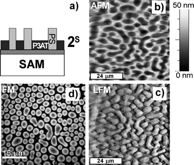
The results shown in Fig. 1 and Fig. 2, pointing to preferential P3DDT adsorption, suggest that the substrate micro-pattern Au/SAM should align the domains of P3DDT/PS. Such a symmetric template of hexadecanethiols, with alternating Au and SAM stripes and periodicity λ = 4 µm, was micro-contact printed35 on a gold substrate. After spin-casting the blend onto the pattern, the micrographs of Fig. 3 were recorded. As in Fig. 2, they indicate lateral domain arrangement (verified by dSIMS). PS and P3DDT phases, now aligned in a grid pattern, are elevated and lowered, respectively, as confirmed by LFM: the P3DDT phase (with higher LFM signal) forms depressed linear domains in register with the bare Au stripes, with sporadic links of P3DDT bridges positioned across the SAM stripes (Fig. 3b and c). Nearly perfect pattern-directed alignment of the (fluorescent) P3AT domains, visible over broad areas (>100 µm) on FM image (Fig. 3d), is limited only by the sample size. This alignment is due to the spatial match33 between pattern periodicity λ and inherent domain scale 2R = 4.1 ± 0.1 µm adjusted by the spinning speed ω. Also the blend morphology reproduces closely the substrate pattern. This feature is characteristic for blends with inherent domain structure close to the bicontinuous morphology (Fig. 2b and c), demonstrated for the films cast on homogeneous (SAM) surfaces.33
 | ||
| Fig. 3 Schematic sectional view (a) of PS/P3DDT blend film spin cast from chloroform onto the substrate micro-pattern of Au/SAM (2 µm/2 µm). The blend film morphology is determined based on AFM (b), LFM (c) and FM (d) micrographs and SIMS profiles (not shown). | ||
B. R-P3HT/PS blends aligned by silanes micro-printed on oxidized silicon
In the second set of experiments, PS blended with regioregular R-P3HT was spin-cast from chloroform on a SAM-covered substrate and on oxidized silicon (a native layer of SiOx). A lamellar domain arrangement LT with continuous upper P3AT-rich lamella and PS-rich bottom layer is found for the R-P3HT/PS films on SAMs, when AFM and dSIMS data are compared (Fig. 4). | ||
| Fig. 4 Schematic sectional view (a) of the lamellar morphology LT for PS/R-P3HT blend films cast from chloroform onto a SAM substrate. The structure is determined based on AFM (b) and dSIMS (c) data. The sputtering time in (c) is a measure of the distance from the free surface (1 sec ≈ 0.12 and 0.15 nm for PS and R-P3HT, respectively). | ||
In turn, lateral structures are visible on the micrographs in Fig. 5, recorded for the blend on SiOx: isolated islands seen in the AFM images, with only a slightly lower LFM signal, are identified by FM as (isolated) fluorescent domains rich in R-P3HT. A lateral domain arrangement 2T with elevated R-P3HT and depressed PS phases, extending throughout the film, is concluded.
 | ||
| Fig. 5 Schematic sectional view (a) of the lateral structure 2T with elevated P3AT-rich phase determined for PS/R-P3HT blend films spin cast from chloroform onto an oxidized silicon substrate. The determination of the structure 2T is based on AFM (b), LFM (c) and FM (d) images, as well as dSIMS profiles (not shown). | ||
In contrast to other P3AT/PS mixtures, the decisive force driving self-organization here is the difference in surface energy (Δγ = 19.7 mJ m−2) between the blend components, distinctly larger than for P3DDT/PS (∼4 times) and P3BT/PS (∼2 times). This force favours the lamellar structure LT with the top layer composed of a P3AT-rich phase, the component with a lower surface energy. Indeed, the LT morphology is observed exclusively in the spin-cast films of R-P3HT/PS blends. However, the phase rich in R-P3HT can also be engaged in competitive processes of deposition and spreading at the substrate. The latter is expressed by the spreading coefficient of R-P3HT on SiOx (S = 12.7 mJ m−2) and on SAM-covered substrates (S = −2.0 mJ m−2). The positive S value indicates a strong tendency for the R-P3HT phase to wet SiOx, in addition to spreading at the free surface. As a result of the phase separation with the same phase preferred at both film surfaces the lateral domain arrangement (2T) is formed instead of the lamellar structure (Fig. 5).54 In turn, the competitive wetting of R-P3HT on SAM-covered substrates is not present, since the S value is negative. Therefore, the lamellar morphology LT emerges from the self-organization (Fig. 4).54a
It has been recently reported that SAM-covered substrates with methyl end-groups can induce formation of adjacent crystalline R-P3HT regions in the films spin cast from solutions of the purepolymer.10 Apparently, here this mechanism is too weak to create the (reversed) bilayers LS in the films deposited from the blend solutions of R-P3HT with high molecular weight. Recent studies of this system show that crystalline self-assembly has no impact on the overall film structures of the spin-cast blends PS/R-P3HT and PS/R-P3DDT.47b
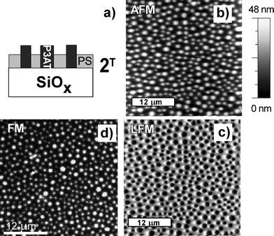
As a consequence of substrate-dependent surface segregation, shown in Fig. 4 and 5, the surface chemically patterned with SiOx/SAM is expected to order the domain structure of the R-P3HT/PS blend. To check this strategy, octadecyltrichlorosilanes were micro-contact printed35 on oxidized silicon to create symmetric templates of alternating SAM and SiOx stripes with the periodicity λ = 8 µm. The micrographs in Fig. 6 show the morphology of the R-P3HT/PS film spin cast (with adjusted spin casting conditions) onto such a pattern. They indicate a lateral domain arrangement, similar to that in Fig. 5 but ordered linearly, with elevated fluorescent R-P3HT domains somewhat wider than the depressed PS phase regions. Pattern-directed alignment of polymer domains extends almost over the macroscopic length scales, as shown by the FM image in Fig. 6d.
 | ||
| Fig. 6 Schematic sectional view (a) of PS/R-P3HT blend film spin cast from chloroform onto the substrate micro-pattern of SiOx/SAM (4 µm/4µm). The blend film morphology is determined based on AFM (b), LFM (c) and FM (d) micrographs and SIMS profiles (not shown). Inset in (d) shows details of the analyzed area. | ||
C. P3BT/PS blends ordered by gold micro-patterned on oxidized silicon
In the third set of experiments, P3BT/PS mixtures were spin cast from cyclohexanone onto continuous gold and oxidized silicon surfaces. For the blend on gold the bilayer structure LS is determined, based on AFM and dSIMS (Fig. 7), with homogeneous PS-rich top and P3BT-rich bottom layers. | ||
| Fig. 7 Schematic sectional view (a) of lamellar structure LS for PS/P3BT blend films spin cast from cyclohexanone onto a Au substrate. The structure is determined based on AFM (b) and dSIMS (c) data. Sputtering time in (c) is a measure of the distance from the free surface (1 sec ≈ 0.20 and 0.27 nm for PS and P3BT respectively). | ||
In contrast, from the micrographs in Fig. 8, recorded for P3BT/PS spin cast on SiOx, we conclude that the lateral domain arrangement 2T is formed. Fluorescent P3BT-rich domains (with lower LFM signal) are finely dispersed and elevated above the matrix rich in PS.
 | ||
| Fig. 8 Schematic sectional view (a) of the lateral structure 2T with an elevated P3BT-rich phase for PS/P3BT blend films spin cast from cyclohexanone onto an oxidized Si substrate. The structure 2T is determined based on AFM (b), LFM (c) and FM (d) images and dSIMS profiles (not shown). | ||
The morphological differences between the P3BT/PS blends spin cast onto various homogeneous surfaces (Fig. 7 and 8) are caused by the preferential adsorption of P3AT onto gold.50,53 This situation is similar to that presented earlier (Fig. 1 and 2), but the force ordering the domains is blocked here by the SiOx substrate rather than by the deposited SAM.
The results of Fig. 7 and 8 indicate that the micro-patterns composed of oxidized silicon and gold should align the domains of spin cast blend P3BT/PS. To verify this suggestion the Au stripes, patterned with the periodicity λ = 4 µm, were fabricated by photo-lithography on a thermally grown SiO2 substrate. After casting the blend onto such a micro-pattern (at adjusted conditions), the micrographs in Fig. 9 were recorded. The overall film morphology corresponds to a lateral domain arrangement (corroborated by dSIMS) similar to that in Fig. 8. In contrast to the situation on oxidized silicon, the dispersed circular (fluorescent) P3BT domains (darker on LFM images) are now aligned by the Au stripes (Figs. 9b and c) over broad areas (Fig. 9d). Similar pattern-directed ordering of droplet-type morphologies was observed earlier for spin-cast blends of dielectric polymers.33 In addition, FM micrographs show a novel feature: the fluorescent signal originates not only from circular P3BT islands (cf. the inset to Fig. 9d and Fig. 9b and c) but also from adjacent regions positioned on the Au bands. This indicates that the phase rich in P3AT also forms the cuticles, which are adsorbed onto the gold substrate regions, but do not extend throughout the polymer film to the free surface.
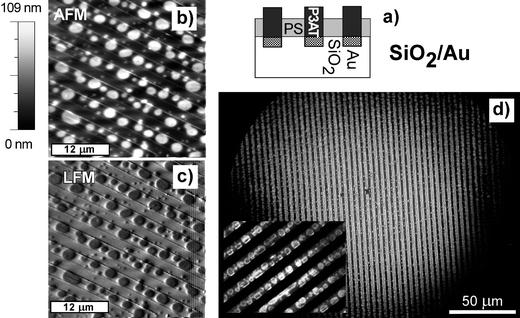 | ||
| Fig. 9 Schematic sectional view (a) of a PS/P3BT blend film spin cast from cyclohexanone onto the substrate micro-pattern of oxidized Si/Au (with 4 µm periodicity). Film morphology is determined based on AFM (b), LFM (c) and FM (d) micrographs, as well as dSIMS profiles (not shown). Inset in (d) shows details of the analyzed area. | ||
III. Experimental
Polymer materials
Polymers used in this work were PS (molecular weight Mw = 65K, polydispersity index Mw/Mn = 1.02), provided by Polymer Standard Service, Mainz, and three different P3ATs purchased from Aldrich Chemical Co: poly(3-butylthiophene) (P3BT) and poly(3-dodecylthiophene) (P3DDT) were both reported by the supplier to have the 1 : 1 ratio of head-to-head : head-to-tail (HT) linkages. In turn, regioregular poly(3-hexylthiophene) (R-P3HT, Mw ≈ 87K) was specified by HT regioregularity >98.5%.Substrates
Silicon wafers with native oxidized silicon layers (SiOx) were cleaned by sonicating in toluene and dried with a nitrogen stream. Gold surfaces were produced by thermal evaporation of (∼50 nm thick) Au layers on silicon wafers.26b,33a,33b To obtain homogeneous surfaces of SAM with methyl end-groups, the Au-covered Si wafers were immersed (for 3 min) in (10 mM) ethanol solution of hexadecanethiol CH3(CH2)15SH.26b,33a,33b They were used as a SAM reference for both the patterns Au/SAM and SiOx/SAM (SAMs formed by CH3(CH2)15SH25,55 and CH3(CH2)17SiCl356 have similar surface energies). The Au/SAM stripe patterns (with 2 µm/2 µm dimensions) were micro-contact printed35 on gold surfaces with a rubber stamp inked with hexadecanethiol in ethanol (see previous works for details).28b,29b,33a,33b,34 In turn, micro-contact printing35 of oxidized silicon surfaces at the atmosphere with controlled relative humidity, performed with a stamp inked with octadecyltrichlorosilane CH3(CH2)17SiCl3 in toluene, resulted in SiOx/SAM (4 µm/4 µm) stripe patterns (for the recipe see ref. 28e, 57). The substrate patterns SiO2/Au (with periodicity λ = 4 um) were fabricated58 by successive steps of (i) thermal growth of (∼300 nm) thick SiO2 layer (Piranha cleaning; then dry oxidation at 1100 °C for 3 h), (ii) resist (AZ5214) coating, (iii) photo-lithography (a broad-band mask aligner), (iv) dry etching (RIE with CHF3 for 3 min), (v) Au deposition (90 nm thick film on a 5 nm thick Cr layer) and (vi) lift off (acetone in ultrasonic bath).Polymer blend films
The polymers were used as obtained to prepare symmetric (1:1 mass fractions of P3AT:PS) binary blends dissolved at constant concentration (CP = 20 mg/mL) in analytic grade common solvents: chloroform (for P3DDT/PS and R-P3HT/PS) and cyclohexanone (for P3BT/PS). Blend films were prepared from the solutions by spin casting (for 30 s, with a spincoater KW-4A, Chemat Technology) onto homogeneous surfaces and substrate micro-patterns. In the latter case the coating speed ω was adjusted carefully to obtain the best possible pattern transposition into the blend morphology.Microscopic characterization of blend films
Topography and friction surface images (scan range up to 60 µm × 60 µm) of the spin-cast blend films were collected in air at room temperature by atomic (AFM) and lateral (LFM) force microscopy (The Academia System, Nanonics Imaging Ltd., Israel) working in contact mode. Fluorescence microscopy (FM) (Olympus Reflected Fluorescence System) was used to obtain the micrographs (imaged area up to 370 µm × 490 µm) of P3AT domains with a Hg illumination source and fluorescence mirror units U-MNB2 (excitation filter transmitting light at 470–490 nm and a 520 nm low pass filter) or U-MNG2 (excitation filter at 530–550 nm and a 590 nm low pass filter) matching the P3AT absorption spectrum.Dynamic secondary ion mass spectrometry
Vertical phase domain arrangement in the films was determined with the depth profiling (depth resolution of ∼10 nm)49 mode of dynamic secondary ion mass spectrometry (dSIMS). The data were obtained with a VSW apparatus equipped with a high-resolution ion gun (liquid metal, Fei Co.) and a Balzers quadrupole mass spectrometer. A primary Ga+ ion beam (5–25 keV, 0.2–4 nA) was used to sputter the sample and to induce secondary ions, which yielded mass-resolved information for the depth profiles. Mapping dSIMS mode was used to test the quality of the substrate micro-patterns SiO2/Au obtained by photo-lithography.IV. Conclusions
This paper describes an extension of blend spin casting combined with a non-reactive methodology for polymer patterning; it demonstrates that metal and oxidized silicon substrates, patterned chemically with micro-contact printing or photo-lithography, can align (over broad areas) the laterally arranged blend domains of conjugated and dielectric polymers. This can provide a simple, solution-processing method to produce thin films with polymer-based circuitries38c and to integrate them into silicon-based electronics, fabricated on the substrate. For instance, lateral continuous domain structures with straight (Fig. 6) and more complex line-shapes could form electric current paths.8,37a Arrangements of droplet-type lateral domains (Fig. 9) ordered into 2-dimensional lattices (e.g. on multi-component surface templates)38c might result in arrays of LED pixels,44 photonic structures36,59 or light-detecting position sensors.60 In turn, self-stratified structures (Fig. 4) which are controlled laterally38 (with asymmetric patterns ordering asymmetric blends) could create assemblages of FETs38c or RC filters.61 Such strategies, employing patterned lateral (this work) and lamellar38 blend structures, could be used to fabricate complexes of electronic components or their connections. This is a first step towards the self-assembly of the all-polymer circuitries in a single process, enabled by a more general approach possibly using molecular recognition.38cThe strategy of pattern-guided self-organization is presented for the spin cast PS blends with three representatives from the heavily studied P3AT family of semiconducting polymers. Substrate-dependent surface segregation, concluded for P3BT/PS and P3DDT/PS on Au and for R-P3HT/PS on SAM, drives the observed blend micro-patterning. Reported recently specific forces between Au and the thiophene groups of other polymers50,53 raise hopes for similar patterning recipes for a wider class of spin cast polythiophene blends.
Ordering with chemically patterned substrates obtained for the spin cast blends of conjugated P3ATs, is not much different from that studied thoroughly earlier for the model polymer mixtures.24,28–31 Therefore the previous observations on compositional33,34 and spatial24,33 commensurability between the pattern and the blend could be used to develop strategies aiming at optimal pattern transposition, also into the more complex film structures and to length scales smaller than the original micro-patterns.34 For instance, the mismatch between blend composition and patterned area fraction controls the extent of preferential segregation. As a result it determines different template-aligned lamellar38 and lateral structures,33 the latter with continuous33a,34 or droplet-like33a,33b domains. Also hierarchical film morphologies with two length scales, reflecting regularly arranged continuous domains and much smaller droplets (due to secondary phase separation), are observed.29b,33a,33c Therefore a surface micro-template with a patterned area fraction, which is laterally varied, should impose the alignment of different structural types into a single spin-cast film. An additional parameter to control film morphology is the commensurability between inherent domain scale 2R and pattern periodicity λ.24,32–34 While simple periodic arrays are formed in blends spin-cast with 2R ≈ λ,24,32,33 hierarchical lateral structures with quantized morphological modes (and length scales λ/n, with n an integer) are observed for 2R < λ.32–34 Then, a decrease in patterned area fraction (and a smaller extent of preferential segregation) induces complete extinction of the fundamental mode λ, i.e. formation of lateral film structures ordered with a sub-pattern periodicity.34 Therefore, spin-casting blends onto surface patterns with laterally varied periodicity λ or patterned area fraction should form regions of ordered lateral structures with different length scales or different periodicities in a single film. Application of more complex surface templates should increase the ability of blend spin-casting to produce film structures with technologically more useful architectures.
Acknowledgements
This work was partially supported by the European Community (under the Marie Curie Host Fellowships for the Transfer of Knowledge, project NEED, contract No. 21/MTKD-CT-2004–003132), the Greek-Polish bilateral cooperation agreement, the Polish Ministry of Science and Higher Education and the Reserve of the Faculty of Physics, Astronomy and Applied Computer Science of the Jagiellonian University.References
- R. H. Reuss, D. G. Hopper and J.-G. Park, MRS Bulletin, 2006, 6, 447.
- S. R. Forrest, Nature, 2004, 428, 911 CrossRef CAS.
- N. Tessler, Adv. Mater., 1999, 11, 363 CrossRef CAS.
- M. D. McGehee and A. J. Heeger, Adv. Mater., 2000, 12, 1655 CrossRef CAS.
- M. Gaal, C. Gadermaier, H. Plank, E. Moderegger, A. Pogantsch, G. Leising and E. J. W. List, Adv. Mater., 2003, 15, 1165 CrossRef CAS.
- R. H. Friend, R. W. Gymer, A. B. Holmes, J. H. Burroughes, R. N. Marks, C. Taliani, D. D. C. Bradley, D. A. Dos Santos, J. L. Brédas, M. Lögdlund and W. R. Salaneck, Nature, 1999, 397, 121 CrossRef CAS.
- C. J. Brabec, N. S. Sariciftci and J. C. Hummelen, Adv. Funct. Mater., 2001, 11, 15 CrossRef CAS.
- H. Sirringhaus, T. Kawase, R. H. Friend, T. Shimoda, M. Inbasekaran, W. Wu and E. P. Woo, Science, 2000, 290, 2123 CrossRef CAS.
- C. D. Dimitrakopolous and P. R. L. Makenfant, Adv. Mater., 2002, 14, 99 CrossRef CAS.
- (a) H. Sirringhaus, N. Tessler and R. H. Friend, Science, 1998, 280, 1741 CrossRef CAS; (b) H. Sirringhaus, P. J. Brown, R. H. Friend, M. M. Nielsen, K. Bechgaard, B. M. W. Langeveld-Voss, A. J. H. Spiering, R. A. J. Janssen, E. W. Meijer, P. Herwig and D. M. de Leeuw, Nature, 1999, 401, 685 CrossRef CAS; (c) R. J. Kline, M. D. Mcgehee and M. F. Toney, Nature Mat., 2006, 5, 222 CrossRef; (d) D. H. Kim, J. T. Han, Y. D. Park, Y. Jang, J. H. Cho, M. Hwang and K. Cho, Adv. Mat., 2006, 18, 719 CrossRef CAS.
- C. J. Lawrence, Phys. Fluids, 1988, 31, 2786 CrossRef CAS , and references therein.
- (a) S. Holdcroft, Adv. Mater., 2001, 13, 1753 CrossRef CAS , and references therein; (b) X. Wang, K. Tvingstedt and O. Inganäs, Nanotechnology, 2005, 16, 437 CrossRef CAS.
- P. Leclere, M. Surin, P. Brocorens, M. Cavallini, F. Biscarini and R. Lazzaroni, Mat. Sci. Eng., 2006, R55, 1 Search PubMed , and references therein.
- E. Menard, M. A. Meitl, Y. Sun, J.-U. Park, D. J.-L. Shir, Y. S. Nam, S. Jeon and J. A. Rogers, Chem. Rev., 2007, 107, 1117 CrossRef CAS , and references therein.
- C. B. Gorman, H. A. Biebuyck and G. M. Whitesides, Chem. Mater., 1995, 7, 526 CrossRef CAS.
- M. L. Renak, G. C. Bazan and D. Roitman, Adv. Mater., 1997, 9, 392 CrossRef.
- Z. Bao, Y. Feng, A. Dodabalapur, V. R. Raju and A. J. Lovinger, Chem. Mater., 1997, 9, 1299 CrossRef CAS.
- T. Granlund, T. Nyberg, L. S. Roman, M. Svensson and O. Inganäs, Adv. Mater., 2000, 12, 269 CrossRef CAS.
- M. Berggren, O. Inganäs, G. Gustafsson, J. Rasmusson, M. R. Andersson, T. Hjertberg and O. Wennerström, Nature, 1994, 372, 444 CrossRef CAS.
- J. M. Halls, C. A. Walsh, N. C. Greenham, E. A. Marsegila, R. H. Friend, S. C. Moratti and A. B. Holmes, Nature, 1995, 376, 498 CrossRef CAS.
- E. Moons, J. Phys.: Condens. Matter, 2002, 14, 12235 CrossRef CAS.
- L.-L. Chua, P. K. H. Ho, H. Sirringhaus and R. H. Friend, Adv. Mater., 2004, 16, 1609 CrossRef CAS.
- N. Corcoran, A. C. Arias, J. S. Kim, J. D. MacKenzie and R. H. Friend, Appl. Phys. Lett., 2003, 82, 299 CrossRef.
- M. Böltau, S. Walheim, J. Mlynek, G. Krausch and U. Steiner, Nature, 1998, 391, 877 CrossRef CAS.
- S. Walheim, M. Böltau, J. Mlynek, G. Krausch and U. Steiner, Macromolecules, 1997, 30, 4995 CrossRef CAS.
- (a) J. S. Gutmann, P. Müller-Buschbaum and M. Stamm, Faraday Discuss., 1999, 112, 258 Search PubMed; (b) A. Budkowski, A. Bernasik, P. Cyganik, J. Raczkowska, B. Penc, B. Bergues, K. Kowalski, J. Rysz and J. Janik, Macromolecules, 2003, 36, 4060 CrossRef CAS.
- S. Y. Heriot and R. A. L. Jones, Nature Mater., 2005, 4, 782 CrossRef CAS.
- (a) G. Krausch, E. J. Kramer, M. H. Rafailovich and J. Sokolov, Appl. Phys. Lett., 1994, 64, 2655 CrossRef CAS; (b) P. Cyganik, A. Bernasik, A. Budkowski, B. Bergues, K. Kowalski, J. Rysz, J. Lekki, M. Lekka and Z. Postawa, Vacuum, 2001, 63, 307 CrossRef CAS; (c) S. Walheim, C. Schäffer and U. Steiner, Surf. Interf. Analys., 2004, 36, 195 Search PubMed; (d) X. Li, R. Xing, Y. Zhang, Y. Han and L. An, L Polymer, 2004, 45, 1637 Search PubMed; (e) L. Cui, Z. Zhang, X. Li and Y. Han, Polymer Bulletin, 2005, 55, 131 CrossRef CAS.
- (a) M. Sprenger, S. Walheim, C. Schäffer and U. Steiner, Adv. Mater., 2003, 15, 703 CrossRef CAS; (b) P. Cyganik, A. Budkowski, U. Steiner, J. Rysz, A. Bernasik, S. Walheim, Z. Postawa and J. Raczkowska, Europhysics Letters, 2003, 62, 855 Search PubMed.
- (a) L. Rockford, Y. Liu, P. Mansky, T. P. Russell, M. Yoon and S. G. J. Mochrie, Phys. Rev. Lett., 1999, 82, 2602 CrossRef CAS; (b) J. Jerome, S. Zhu, Y. S. Seo, M. Ho, N. Pernodet, R. Gambino, J. Sokolov, M. H. Rafailovich, V. Zaitsev, S. Schwarz and R. DiNardo, Macromolecules, 2004, 37, 6504 CrossRef CAS; (c) C. Minelli, I. Geissbuehler, R. Eckert, H. Vogel, H. Heinzelmann and M. Liley, Colloid. Polym. Sci., 2004, 282, 1274 CrossRef CAS.
- K. Fukunaga, H. Elbs and G. Krausch, Langmuir, 2000, 16, 3474 CrossRef CAS.
- (a) A. Karim, J. F. Douglas, B. P. Lee, S. C. Glotzer, J. A. Rogers, R. J. Jackman, E. J. Amis and G. M. Whitesides, Phys. Rev. E, 1998, 57, R6273 Search PubMed; (b) B. D. Ermi, G. Nisato, J. F. Douglas, J. A. Rogers and A. Karim, Phys. Rev. Lett., 1998, 81, 3900 CrossRef CAS; (c) G. Nisato, B. D. Ermi, J. F. Douglas and A. Karim, Macromolecules, 1999, 32, 2356 CrossRef CAS.
- (a) J. Raczkowska, P. Cyganik, A. Budkowski, A. Bernasik, J. Rysz, I. Raptis, P. Czuba and K. Kowalski, Macromolecules, 2005, 38, 8486 CrossRef CAS; (b) J. Raczkowska, A. Bernasik, A. Budkowski, P. Cyganik, J. Rysz, I. Raptis and P. Czuba, Surface Science, 2006, 600, 1011; (c) P. Andrew and W. T. S. Huck, Soft Matter, 2007, 3, 230 RSC.
- J. Raczkowska, A. Bernasik, A. Budkowski, J. Rysz, B. Gao and M. Lieberman, Macromolecules, 2007, 40, 2120 CrossRef CAS.
- (a) Y. Xia and G. M. Whitesides, Angew. Chem., Int. Ed., 1998, 37, 550 CrossRef CAS; (b) B. D. Gates, Materials Today, 2005, 8, 44 CrossRef CAS; (c) S. A. Ruiz and C. S. Chen, Soft Matter, 2007, 3, 1 RSC.
- (a) G. Fichet, N. Corcoran, P. K. H. Ho, A. C. Arias, J. D. MacKenzie, W. T. S. Huck and R. H. Friend, Adv. Mater., 2004, 16, 1908 CrossRef CAS; (b) N. Corcoran, P. K. H. Ho, A. C. Arias, J. D. MacKenzie, R. H. Friend, G. Fichet and W. T. S. Huck, Appl. Phys. Lett., 2004, 85, 2965 CrossRef CAS.
- (a) J. Haberko, J. Raczkowska, A. Bernasik, J. Rysz, A. Budkowski and W. Łużny, Synthetic Metals, 2007, 157, 935 Search PubMed; (b) F. C. Chen, Y. K. Lin and C. J. Ko, Appl. Phys. Lett., 2008, 92 Search PubMed 023307.
- (a) D. C. Coffey and D. S. Ginger, J. Am. Chem. Soc., 2005, 127, 4565; (b) J. H. Wei, D. C. Coffey and D. S. Ginger, J. Phys. Chem. B, 2006, 110, 24324 CrossRef CAS; (c) A. Salleo and A. C. Arias, Adv. Mater., 2007, 19, 3540 CrossRef CAS.
- H. Hoppe and N. S. Sariciftci, J. Mat. Chem., 2006, 16, 45 RSC , and references therein.
- H. Sirringhaus, Adv. Mat., 2005, 17, 2411 CrossRef CAS , and references therein.
- J. T. Mabeck and G. C. Malliaras, Anal. Bioanal. Chem., 2006, 384, 343 CAS , and references therein.
- A. Salleo, Materials Today, 2007, 10, 38 CrossRef CAS.
- (a) A. Proń and P. Rannou, Prog. Polym. Sci., 2002, 27, 135 CrossRef CAS; (b) J. Jaczewska, I. Raptis, A. Budkowski, D. Goustouridis, J. Raczkowska, M. Sanopoulou, E. Pamuła, A. Bernasik and J. Rysz, Synthetic Metals, 2007, 157, 726 Search PubMed.
- (a) M. Granström and O. Inganäs, Appl. Phys. Lett., 1996, 68, 147 CrossRef; (b) M. Granström, M. Berggren, D. Pede, O. Inganäs, M. R. Andersson, T. Hjertberg and O. Wennerström, Supramol. Sci., 1997, 4, 27 CrossRef; (c) X. Han, X. Chen and S. Holdcroft, Adv. Mater., 2007, 19, 1697 CrossRef CAS.
- (a) A. C. Arias, F. Endicott and R. A. Street, Adv. Mater., 2006, 18, 2900 CrossRef CAS; (b) L. Qiu, J. A. Lim, X. Wang, W. H. Lee, M. Hwang and K. Cho, Adv. Mater., 2008, 20, 1141 CrossRef CAS.
- (a) S. Goffri, C. Müller, N. Stingelin-Stutzmann, D. W. Breiby, C. P. Radano, J. W. Andreasen, R. Thompson, R. A. J. Janssen, M. N. Nielsen, P. Smith and H. Sirringhaus, Nature Mat., 2006, 5, 950 CrossRef CAS; (b) G. Lu, H. Tang, Y. Qu, L. Li and X. Yang, Macromolecules, 2007, 40, 6571.
- (a) J. Jaczewska, A. Budkowski, A. Bernasik, I. Raptus, J. Raczkowska, D. Goustouridis, J. Rysz and M. Sanopoulou, J. Appl. Polymer Sci., 2007, 105, 67 CrossRef CAS; (b) J. Jaczewska, A. Budkowski, A. Bernasik, E. Moons and J. Rysz, Macromolecules, 2008, 41, 4802 CrossRef CAS.
- S. Nilsson, A. Bernasik, A. Budkowski and E. Moons, Macromolecules, 2007, 40, 8291 CrossRef CAS.
- A. Bernasik, J. Rysz, A. Budkowski, K. Kowalski, J. Camra and J. Jedliński, Macromol. Rapid Comm., 2001, 22, 829 CrossRef CAS.
- C. M. Björström, S. Nilsson, A. Bernasik, A. Budkowski, M. Andersson, K. O. Magnusson and E. Moons, Appl. Surf. Sci., 2007, 253, 3906 CrossRef.
- (a) A. Bernasik, J. Włodarczyk-Miśkiewicz, W. Łużny, K. Kowalski, J. Raczkowska, J. Rysz and A. Budkowski, Synthetic Metals, 2004, 144, 253 Search PubMed; (b) A. Bernasik, J. Haberko, J. Włodarczyk-Miśkiewicz, J. Raczkowska, W. Łużny, A. Budkowski, K. Kowalski and J. Rysz, Synthetic Metals, 2005, 155, 516 Search PubMed.
- C. Ton-That, A. G. Shard, D. O. H. Teare and R. H. Bradley, Polymer, 2001, 42, 1121 CrossRef CAS.
- T. Matsuura, H. Sakaguchi and Y. Shimoyama, J. Mater. Sci.: Mater. El., 2003, 14, 353 Search PubMed.
- (a) K. Binder, P. Nielaba and V. Pereyra, Z. Phys. B, 1997, 104, 81 CrossRef CAS; (b) A. Bernasik, J. Rysz, A. Budkowski, R. Brenn, K. Kowalski, J. Camra and J. Jedliński, Eur. Phys. J., 2003, 12, 211 CAS.
- B. Bergues, J. Lekki, A. Budkowski, P. Cyganik, M. Lekka, A. Bernasik, J. Rysz and Z. Postawa, Vacuum, 2001, 63, 297 CrossRef CAS.
- (a) D. Janssen, R. De Palma, S. Verlaak, P. Heremans and W. Dehaen, Thin Solid Films, 2006, 215, 1433 CrossRef; (b) M. K. Chaudhury and G. M. Whitesides, Langmuir, 1991, 7, 1013 CrossRef CAS.
- (a) Z. Zhang, Z. Wang, R. Xing and Y. Han, Polymer, 2003, 44, 3737 CrossRef CAS; (b) Z. Zhang, Z. Wang, R. Xing and Y. Han, Surface Science, 2003, 539, 129 CrossRef CAS.
- W. M. Moreau, Semiconductor Lithography: Principles, Practices and Materials, Springer, New York, 1987 Search PubMed.
- R. Riehn and F. Cacialli, J. Opt. A.: Pure Appl. Opt., 2005, 7, S207 CrossRef.
- D. Kabra, Th. B. Singh and K. S. Narayan, Appl. Phys. Lett., 2004, 85, 5073 CrossRef CAS.
- B. Chen, T. Cui, Y. Liu and K. Varahramyan, Solid State Electron., 2003, 47, 841 CrossRef CAS.
| This journal is © The Royal Society of Chemistry 2009 |