A simple, optically induced electrokinetic method to concentrate and pattern nanoparticles
Stuart J.
Williams
a,
Aloke
Kumar
a,
Nicolas G.
Green
b and
Steven T.
Wereley
*a
aPurdue University, Birck Nanotechnology Center, 1205 W State Street, West Lafayette, Indiana 47907, USA. E-mail: wereley@purdue.edu; Fax: +1 765-496-6443; Tel: +1 765-494-5624
bSchool of Electronics and Computer Science, University of Southampton, Highfield, Southampton, SO17 1BJ, UK. E-mail: ng2@ecs.soton.ac.uk
First published on 13th August 2009
Abstract
We demonstrate an optically induced electrokinetic technique that continuously concentrates nanoparticles on the surface of a parallel plate electrode that is biased with an AC signal. A highly focused beam of near-infrared light (1064 nm) was applied, inducing an electrothermal microfluidic vortex that carried nanoparticles to its center where they were accumulated. This technique was demonstrated with 49 nm and 100 nm fluorescent polystyrene particles and characterized as a function of applied AC frequency and voltage. With this technique the location and shape of colloidal concentration was reconfigured by controlling the optical landscape, yielding dynamic control of the aggregation. Colloidal concentration was demonstrated with a plain parallel plate electrode configuration without the need of photoconductive materials or complex microfabrication procedures.
Introduction
The ability to concentrate and pattern an aggregation of nanoparticles is important for the development of artificial architectures including colloidal crystals1 or to accumulate analytes for enhanced sample detection and diagnosis. Several optical, thermal, and electrokinetic techniques have been developed to concentrate nanoparticles. Optical trapping of sub-100 nm particles poses a practical challenge,2,3 not just because Brownian motion imparts large random velocities, but optical trapping forces are scaled with the volume of the particle. A prohibitively high laser power requirement for trapping nanoparticles has led to the development of novel optical tweezing methodologies; for example, utilizing the high polarizability of metallic particles to trap gold nanoparticles.4Optically induced simultaneous thermophoresis and convection has been used to concentrate DNA;5 however, increased temperature (>50 K) was necessary for aggregation. Dielectrophoresis has been applied to accumulate and even separate nanoparticles;6 however, careful consideration of electrode design is necessary as the dielectrophoretic force scales with the volume of the particle. Moreover, as with many similar electrokinetic techniques, the location of the particle aggregations is limited to permanently patterned electrode features and therefore the location of concentrated particles cannot be dynamically positioned. A voltage feedback system can be incorporated with these electrokinetic techniques to position particles,7 but with added complexity. Recently, photoconductive materials have been coupled with illumination patterns to induce AC electroosmosis, offering dynamic and controlled translation of particles.8Recently, we have introduced an optically induced, AC electrokinetic technique called rapid electrokinetic patterning (REP) that can rapidly accumulate, translate, and pattern particles and collect them in a crystalline-like monolayer assembly without the need for photoconductive materials.9 This technique was applied to polystyrene, latex, and silica particles with diameters of 500 nm and larger. Here, we expand upon our initial investigation to concentrate and pattern 49 nm and 100 nm polystyrene particles on the surface of indium tin oxide (ITO) and gold electrodes. Highly focused near-infrared (1064 nm) illuminations were applied with an applied laser power less than 0.4 W. We showcase its rapid concentration time and characterize this technique as a function of applied AC voltage and frequency.
In general, optically induced electrokinetic techniques offer a degree of flexibility and dynamic control that exceed traditional electrokinetic techniques driven by permanent microelectrode features. Advances in optical trapping technology have enabled holographic landscapes that are implemented by a computer-controlled spatial light modulator, producing light patterns that are easily repeatable and reconfigurable.10 We have applied these highly focused computer-generated holograms to drive our optically induced electrokinetic technique, yielding precise, high resolution control of illumination landscapes necessary to concentrate and pattern nanoparticles. Unlike current opto-electronic techniques,8,11REP does not use photoconductive materials to optically induce electrokinetic phenomena. Instead, our technique applied near-infrared optical landscapes to induce fluid motion for particle concentration on one surface of a plain parallel plate electrode.
Experiment and methods
Our optically induced electrokinetic technique is illustrated in Fig. 1. A liquid sample containing colloids was introduced between two, parallel plate electrodes. The electrode closest to the illumination source was a glass cover slip coated with ITO, allowing optical access to the opposite electrode surface. These electrodes were biased with an AC signal with frequencies typically less than 100 kHz. The experimental area was located such that the parallel plate electrode spacer does not significantly influence the electric field. | ||
| Fig. 1 Illustration of our rapid electrokinetic patterning technique. Suspended particles were introduced between two parallel plate electrodes biased with an AC signal. Optical landscapes are applied at 1064 nm to one electrode surface. The illumination creates thermal gradients, inducing an electrothermal microvortex, bringing particles towards its center. Low-frequency electrokinetics concentrates and patterns the particles. | ||
The applied, highly focused 1064 nm illumination locally heats the fluid sample, generating thermal gradients. This produces gradients in the dielectric properties of the fluid (permittivity and conductivity). An applied electric field will act upon these non-uniformities, inducing a body force on the fluid.12 This optically induced electrothermal fluid motion has been investigated previously, and fluid velocities over 100 µm s−1 have been achieved.13 Although the electric field by itself generates heat (Joule heating), our optical illumination is the dominant source of non-uniform heat due to the highly-focused light patterns that vary radically in intensity over a few micrometres. For our experimental setup, the resulting fluid flow profile is toroidal, with the center of the recirculation located at the laser focal point (Fig. 1).14 The velocity of the microvortex depends on the illumination intensity, the dielectric properties of the medium, and the voltage and frequency of the applied AC signal.14 Further, holographic methods allow for more complex, highly focused optical landscapes to be applied, resulting in microfluidic circulation patterns resembling the programmed illumination.
This microfluidic vortex carries particles towards its center on the electrode surface where they aggregate. The electrokinetic mechanisms responsible for particle concentration are AC frequency dependent. Low-frequency planar colloidal aggregate formation and patterning was demonstrated originally by Trau et al.15 and since has been extensively investigated.16–18 Their formation was attributed to induced electrohydrodynamic flows on the surface of the electrode that carry particles towards each other. This induced flow occurs when the low-frequency electric field is locally disturbed from the presence of the electrical double-layer of the particle. As the frequency increases, the double-layer polarization reaches its relaxation frequency, occurring at frequencies much lower than the interfacial Maxwell–Wagner polarization typically associated with dielectrophoresis.19 Coupling this electrokinetic behavior with the induced microfluidic vortex results in superlative particle collection rates and patterning capabilities. Furthermore, our previous investigations with larger particles (>500 nm) have shown that colloidal concentrations form crystalline-like monolayer aggregations.9
Chip design and fabrication
The experimental chip consists of a colloidal sample introduced between two parallel plate electrodes (Fig 1). ITO-coated glass cover slips (170 µm thick, SPI Supplies, West Chester, PA, USA) were used for the bottom electrode while the top electrode was made either from sputtered gold and chrome (Au 150 nm–Cr 50 nm) deposited on glass (0.7 mm thick) or a second ITO-coated glass substrate. The height of the chamber was 50 µm and constructed from double-sided adhesive tape (Adhesives Research Inc., Glen Rock, PA, USA) containing microfluidic features. The observed area was placed approximately in the middle of the microfluidic chamber in order to avoid any influence of the spacer wall on the local electric field. An AC signal was then applied between the parallel plate electrodes, resulting in a uniform electric field in the experimental area.Optical system
An inverted microscope equipped with a 100× oil-immersion lens (1.30 NA and 0.16 mm working distance) was used for both visualization and application of the near-infrared optical landscapes. The illumination source is a Nd:YAG laser-based holographic illumination system (Bioryx® 200, Arryx Inc., Chicago, USA) operating at 1064 nm. The maximum emitted laser power was 0.4 W, with only about 15% of this reaching the sample. These strongly focused illumination patterns were used to drive the electrokinetic mechanisms to accumulate and pattern nanoparticles.Particle preparation
Red fluorescent polystyrene particles 49 nm and 100 nm in diameter (Duke Scientific, CA, USA) were used to illustrate nanoparticle concentration and patterning. Nanoparticle solutions were prepared in an aqueous medium of potassium chloride (KCl) containing 0.1% polysorbate 20 (Tween 20). The solution had a measured electrical conductivity of 0.6 mS m−1. Between trials, the AC signal and illumination were deactivated and a fresh sample was injected to prevent interference and photobleaching of the particles. A mercury arc lamp (X-Cite 120 PC, EXFO, Quebec, Canada) and an appropriate filter cube were used to excite the fluorescent particles; the loss of fluorescence due to photobleaching was slightly less than 1% per second. Due to the small size of the nanoparticles and limitations of the optics used, acquired images did not show individual particles; instead, the concentrated particles resembled fluorescent spots on the electrode surface.Image acquisition and analysis
Images were acquired with an interline transfer charge coupled device (CCD) camera (Coolsnap HQ, Photometrics, Roper Scientific Inc.). The camera has a 1392 × 1040 element CCD at a 6.45 µm × 6.45 µm pixel pitch. A MATLAB program determined the center of the fluorescent particle accumulation and analyzed the fluorescence intensity profile as a function of radial position. Fluorescence data points were averaged in steps of whole pixels (64.5 nm) and the resulting fluorescent profile for each applied voltage or frequency was determined.Results and discussion
Fig. 2 shows a set of experimental images acquired on the surface of a gold electrode using REP. First, 100 nm particles were captured with a single, focused spot (Fig. 2a) with a laser power 0.18 W and an AC signal of 10 kHz and 14 Vpk-pk (volts peak-to-peak). The fluorescent particle concentration produced a Gaussian-shaped intensity profile a few micrometres in diameter. Utilizing the capabilities of holography, two additional focused spots were added with a laser power of 0.4 W, resulting in the pattern shown in Fig. 2b. The location of each focused illumination can be dynamically controlled, resulting in the precise translation of concentrated particles. Dynamic and rapid translation of particle aggregates will enhance the performance of sensors and analysis performed at this scale. Similar results were obtained with 49 nm particles; images containing 100 nm fluorescent particles are shown here as they provide clearer, brighter images. | ||
| Fig. 2 Experimental images showing the concentration and patterning of 100 nm fluorescent polystyrene particles on the surface of a gold electrode with 1064 nm optical landscapes. (a) A highly focused beam of light and (b) three focused spots were used to concentrate particles with an AC signal of 10 kHz and 14 Vpk-pk and a laser power of 0.18 W and 0.4 W, respectively. | ||
The rate of particle accumulation on the surface of the gold electrode was investigated with 100 nm particles, a focused illumination spot with laser power of 0.2 W, and an AC signal of 10 kHz and 12.0 Vpk-pk. Images were acquired every 0.2 s after the activation of the AC signal. The amplitude of fluorescence intensity for the concentrated particle group is plotted for a 25 s duration (Fig. 3). Nanoparticle saturation occurs at approximately 12 s before a decrease in intensity due to photobleaching of captured particles.
 | ||
| Fig. 3 The rate of 100 nm polystyrene particle concentration on a gold surface with a laser power of 0.2 W and an AC signal of 10 kHz and 12.0 Vpk-pk. Images were acquired every 0.2 s. | ||
Nanoparticle concentration was characterized as a function of voltage using 100 nm particles concentrated on the surface of the ITO cover slip. A single focused illumination spot was used with an applied laser power of 0.2 W and an AC frequency of 20 kHz. The voltage was arbitrarily set within a range of 3.3 Vpk-pk to 15.2 Vpk-pk in steps of 0.85 Vpk-pk. Images were acquired after five seconds of particle concentration. A MATLAB program determined the center of the accumulation and analyzed the fluorescent intensity as a function of radial position. Fluorescence data points were averaged in steps of whole pixels (64.5 nm) and the resulting profile for each applied voltage was determined (Fig. 4a). As voltage increased the number of concentrated particles increased, observed in both Gaussian profile amplitude and width. No particle concentration occurred at 3.3 Vpk-pk even though microfluidic vortex motion was observed. The linear relationship between the peak fluorescence intensity and the applied voltage is shown in Fig. 4b.
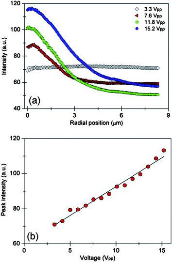 | ||
| Fig. 4 Concentration of 100 nm particles as a function of voltage. (a) Radial profile of fluorescent intensity for a given applied voltage. (b) The peak fluorescence intensity of nanoparticle concentration as a function of voltage. Aggregation occurred on the surface of an ITO electrode with a laser power of 0.2 W and an AC frequency of 20 kHz. | ||
Both the electrothermal microfluidic velocity and electrokinetic forces increase with applied voltage. The velocity of the microfluidic vortex is proportional to voltage squared;12,14 therefore, particles are introduced into the trapping region faster, leading to an enhanced accumulation rate. Furthermore, higher voltages increase the electrokinetic trapping forces. There are a combination of electrokinetic phenomena that may account for nanoparticle concentration including localized AC electroosmosis, induced dipole forces, and electrostatic forces. Future experiments will investigate these potential electrokinetic interactions; it is difficult to determine the dominant electrokinetic force from voltage data alone.
Next, the frequency-dependent concentration of nanoparticles was investigated on the surface of the ITO cover slip with a laser power of 0.2 W and applied voltage of 16.1 Vpk-pk. Fluorescent images were acquired continuously as the frequency was swept from 120 kHz to 10 kHz over an experimental period of 55 s. The fluorescence intensities as a function of radial position for given frequencies are plotted in Fig. 5a. The peak fluorescence intensity of nanoparticle aggregations for the tested frequency range is shown in Fig. 5b. The concentration was negligible at larger frequencies (>100 kHz), as the polarization of the ionic double-layer approached its relaxation frequency; microvortex fluid motion was still observed at these higher frequencies. Nanoparticle accumulation improved with decreasing frequency, reaching a peak value at approximately 50 kHz—the overall fluorescence was influenced by photobleaching as well as the introduction of fresh particles from the microfluidic vortex. Particle concentration decreased at values below this peak frequency. The microfluidic vortex was unable to translate nanoparticles along the electrode surface; they remained unaffected by this hydrodynamic drag and preferred areas on the surface with imperfections, scratches and other similar features that would generate electric field non-uniformities. This evidence shows that local AC electroosmotic forces dominate nanoparticle translation at lower frequencies.
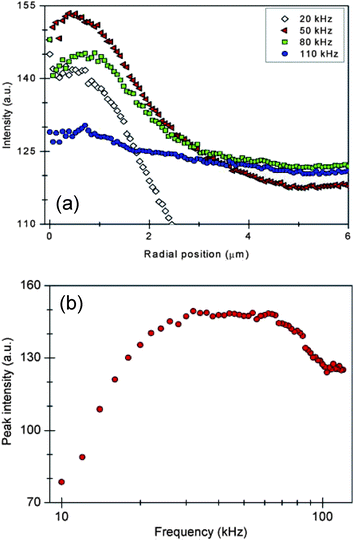 | ||
| Fig. 5 Concentration of 100 nm particles as a function of frequency. (a) Radial profile of fluorescence intensity for given applied frequencies. (b) The peak fluorescence intensity of nanoparticle concentration as a function of frequency. Aggregation occurred on the surface of an ITO electrode with a laser power of 0.2 W and an AC voltage of 16.1 Vpk-pk. | ||
REP requires simultaneous illumination and electric fields in order to concentrate nanoparticles and induce microfluidic motion. If either the illumination or the AC signal is deactivated, the concentrated particles disperse and the concentrated fluorescent spot dissipates. In addition, the microvortex motion would not be observed. If only the illumination is activated, no particle concentration was observed, showing that optical trapping does not occur.
Previous investigations have shown that colloidal patterning can occur on the surface of planar ITO due to inhomogeneous current densities when the ITO film is altered physically20 or with applied ultraviolet illumination.16 For our experiments, nanoparticle aggregation occurred not only on the surface of ITO, but on gold as well. Further, previous investigations have shown that electrothermal hydrodynamics is the mechanism responsible for driving fluid when focused 1064 nm illumination was applied to a liquid exposed to an electric field.13,14 Therefore illumination induced non-uniform current densities minimally contribute to REP.
The electrokinetic motion and aggregation of particles on the surface of an electrode have also been extensively investigated.21–23 The particle–particle and particle–electrode forces are complex and are not completely understood. These electrokinetic phenomena which are responsible for REP are the subject of continued investigation. These forces are a function of AC frequency, electric field magnitude, particle size, electrolyte conductivity, and electrolyte type. Therefore REP should behave differently for a variety of experimental conditions. Future investigations will fully characterize the complex mechanisms of REP, yet our preliminary investigations have showcased its simplistic, continuous concentration capabilities.
The induced electrothermal hydrodynamic motion was not natural fluid convection. First, the heat generated from a highly focused 1064 nm optical trap in water is approximately 1.4 °C–1.9 °C per 100 mW,24 and recall for our experiments that 15% of the laser power (<0.4 W) reached the chip. Furthermore, the microfluidic chamber height was 50 µm and, at heights less than an order of 1 mm, gravity cannot overcome viscous friction.25 The non-uniform thermal gradients produced with the highly focused illumination, and not the absolute increase in temperature, drive this electrothermal fluid motion. Therefore, this nanoparticle concentration technique can be applied to temperature sensitive applications. For the above experiments, thermal gradients were produced by heating the fluid itself with near-infrared illumination. Water does not absorb light in the visible spectrum as readily as it can at 1064 nm;26 however, the fluid can be heated indirectly if the substrate absorbs the illumination. For example, a silver surface can be heated at 300 nm or gold with a 532 nm laser;26 colloids were manipulated with simultaneous optically induced convection and optical traps by Korda et al.27 with a 532 nm holographic system and gold films.
A complex holographic optical trapping unit was utilized in order to pattern nanoparticle aggregations. This system has the capability of producing dynamic and reconfigurable optical landscapes. Essentially, simple particle concentration was achieved with a focused beam of light, similar to conventional optical trapping systems yet with a lower laser power source. A properly aligned and focused illumination source to produce sharp thermal gradients within a parallel plate electrode is all that is needed for REP, although a more complex, inexpensive optical trapping system28 could be adapted.
Conclusions
Nanoparticles were shown to accumulate on both ITO and gold surfaces. Photoconductive materials, necessary for recent advances in opto-electronics,8,11 were not used to induce our technique. This simplifies fabrication and integration with established lab-on-a-chip technologies. Furthermore, nanoparticle concentration on gold surfaces is important as this material can be functionalized with a variety of biological entities.Future experiments will investigate and utilize the frequency-dependent ionic double-layer polarization mechanism driving the electrokinetic trapping forces. This electrokinetic phenomenon is a function of the particle's ionic double-layer and particle diameter. Therefore, particles can be selectively captured and separated by particle type or particle size. Through selective concentration, this technique can be used to enhance a variety of diagnostic lab-on-a-chip applications. The double-layer polarization of colloids can be investigated in a uniform electric field environment, avoiding interfering non-uniform electrokinetic effects like dielectrophoresis6 and AC electroosmosis.
We have introduced a novel optically-induced method that couples electrothermal microfluidic motion with low-frequency electrokinetics for nanoparticle concentration and patterning. Optical methods allow dynamic control over the placement and translation of concentrated colloids. REP is a versatile tool that can be applied to enhance a variety of existing lab-on-a-chip techniques.
Acknowledgements
We would like to acknowledge support from NSF Grant CMMI-0654031. S. J. Williams acknowledges support under a National Science Foundation Graduate Research Fellowship. We thank Dr Robert Keynton at the University of Louisville Center for Micro/Nano Technology and their staff, including Scott Cambron, for access to their facilities and services.References
- S. Noda, and T. Baba, Roadmap on photonic crystals, Kluwer Academic Publishers, Dordrecht, Boston, 2003 Search PubMed.
- R. Conroy, in Handbook of Molecular Force Spectroscopy, ed. A. Noy, Springer US, New York, 2008 Search PubMed.
- A. Rohrbach and E. H. K. Stelzer, Appl. Opt., 2002, 41, 2494 CrossRef.
- K. Svoboda and S. M. Block, Opt. Lett., 1994, 19, 930 Search PubMed.
- D. Braun and A. Libchaber, Phys. Rev. Lett., 2002, 89, 188103 CrossRef.
- N. G. Green and H. Morgan, J. Phys. D: Appl. Phys., 1997, 30, L41 CrossRef CAS.
- A. E. Cohen and W. E. Moerner, Appl. Phys. Lett., 2005, 86, 093109 CrossRef.
- P. Y. Chiou, A. T. Ohta, A. Jamshidi, H. Y. Hsu and M. C. Wu, J. Microelectromech. Syst., 2008, 17, 525 CrossRef.
- S. J. Williams, A. Kumar and S. T. Wereley, Lab Chip, 2008, 8, 1879 RSC.
- D. G. Grier, Nature, 2003, 424, 810 CrossRef CAS.
- P. Y. Chiou, A. T. Ohta and M. C. Wu, Nature, 2005, 436, 370 CrossRef CAS.
- N. G. Green, A. Ramos, A. Gonzalez, A. Castellanos and H. Morgan, J. Phys. D: Appl. Phys., 2000, 33, L13 CrossRef CAS.
- M. Nakano, S. Katsura, G. G. Touchard, K. Takashima and A. Mizuno, IEEE Trans. Ind. Appl., 2007, 43, 232 CrossRef.
- A. Kumar, S. J. Williams and S. T. Wereley, Microfluid. Nanofluid., 2009, 6, 637 CrossRef CAS.
- M. Trau, S. Sankaran, D. A. Saville and I. A. Aksay, Nature, 1995, 374, 437 CrossRef CAS.
- R. C. Hayward, D. A. Saville and I. A. Aksay, Nature, 2000, 404, 56 CrossRef CAS.
- S. R. Yeh, M. Seul and B. I. Shraiman, Nature, 1997, 386, 57 CrossRef CAS.
- M. Trau, D. A. Saville and I. A. Aksay, Science, 1996, 272, 706 CrossRef CAS.
- N. G. Green and H. Morgan, J. Phys. Chem. B, 1999, 103, 41 CrossRef CAS.
- W. D. Ristenpart, P. Jiang, M. A. Slowik, C. Punckt, D. A. Saville and I. A. Aksay, Langmuir, 2008, 24, 12172 CrossRef CAS.
- J. A. Fagan, P. J. Sides and D. C. Prieve, Langmuir, 2005, 21, 1784 CrossRef CAS.
- J. D. Hoggard, P. J. Sides and D. C. Prieve, Langmuir, 2008, 24, 2977 CrossRef CAS.
- Y. Liu, R. G. Xie and X.-Y. Liu, Appl. Phys. Lett., 2007, 91, 063105 CrossRef.
- H. B. Mao, J. R. Arias-Gonzalez, S. B. Smith, I. Tinoco and C. Bustamante, Biophys. J., 2005, 89, 1308 CrossRef CAS.
- A. Gonzalez, A. Ramos, H. Morgan, N. G. Green and A. Castellanos, J. Fluid Mech., 2006, 564, 415 Search PubMed.
- M. J. Weber, Handbook of Optical materials, CRC Press, Boca Raton, 2003 Search PubMed.
- P. T. Korda, G. C. Spalding and D. G. Grier, Phys. Rev. B: Condens. Matter Mater. Phys., 2002, 66, 024504 CrossRef.
- S. P. Smith, S. R. Bhalotra, A. L. Brody, B. L. Brown, E. K. Boyda and M. Prentiss, Am. J. Phys., 1999, 67, 26 CrossRef.
| This journal is © The Royal Society of Chemistry 2009 |