High-pressure needle interface for thermoplastic microfluidics
C. F.
Chen
ab,
J.
Liu
a,
L. P.
Hromada
a,
C. W.
Tsao
a,
C. C.
Chang
b and
D. L.
DeVoe
*a
aDepartment of Mechanical Engineering, Department of Bioengineering, University of Maryland, College Park, MD, USA
bInstitute of Applied Mechanics, National Taiwan University, Taipei 106, Taiwan. E-mail: ddev@umd.edu; Fax: +1 301 314 9477; Tel: +1 301 405 8125
First published on 19th November 2008
Abstract
A robust and low dead volume world-to-chip interface for thermoplastic microfluidics has been developed. The high pressure fluidic port employs a stainless steel needle inserted into a mating hole aligned to an embedded microchannel, with an interference fit used to increase pressure resistance. Alternately, a self-tapping threaded needle screwed into a mating hole is also demonstrated. In both cases, the flat bottom needle ports seat directly against the microchannel substrate, ensuring low interfacial dead volumes. Low dispersion is observed for dye bands passing the interfaces. The needle ports offer sufficient pull-out forces for applications such as liquid chromatography that require high internal fluid pressures, with the epoxy-free interfaces compatible with internal microchannel pressures above 40 MPa.
Introduction
Microfludics technology has been applied to a wide range of analytical systems, including integrated lab-on-a-chip platforms where all analytical processes and functions are combined into a single microfluidic substrate. However, it is often desirable to interface on-chip analysis with off-chip components such as pumps and valves, and benchtop instrumentation for sample preparation, purification, and fractionation. In these cases there is a need for fluidic interfaces capable of seamlessly transfering analytes, reagents, and other solutions between benchtop systems and microfluidic chips.Ideally, world-to-chip interfaces should provide compatible interconnection with capillaries and other tubing commonly used in benchtop analytical instrumentation. From a practical perspective the interconnects should be inexpensive and simple to implement, and suitable both for chip prototyping and commercial fabrication. For applications such as liquid chromatography (LC), interfaces must be compatible with high internal fluid pressures. Another important concern is the potential introduction of unwanted dead volume, which can result in analyte dispersion, delays in fluid transport, excessive reagent usage, and sample carryover between sequential injections into the microfluidic chip. Dead volumes can also act as sites for bubble nucleation and trapping, introducing compliance in the microfluidic system and potentially leading to channel clogging. More generally, large dead volumes can necessitate the introduction of significantly larger volumes of reagents and samples than required for analysis, negating the advantages associated with small on-chip volumes inherent to microfluidic systems.
Due to the wide variety of material, fabrication, and functional requirements of microfluidic systems, no standard world-to-chip interface has emerged.1 For glass microfluidic chips, silica capillaries have been inserted into self-aligned holes drilled into chip sidewalls2 or holes machined into the top surface of a glass substrate,3 with adhesive used to secure the capillaries and prevent fluid leakage past the chip/capillary interface. By taking advantage of high-aspect ratio etching processes for the fabrication of silicon microfluidics, integrated ferrules have been demonstrated for coupling capillaries to silicon chips using either adhesives or plastic retaining elements to hold the assemblies together.4 Similarly, silicon-based ferrules have been designed to couple microchannels with off-chip tubing using heat-shrink polymer to seal both ends of the interconnect.5 A related approach employed for silicon microfluidics used solder bonding between a copper bond pad aligned to an on-chip channel reservoir and a custom off-chip ferrule coated with a low temperature solder film.6
While these methods of forming low dead volume fluidic interfaces with glass and silicon chips rely on modifications to the microfluidic substrates, a variety of manifold assemblies have also been described.7–15 This approach shifts fabrication and assembly constraints from the microfluidic chip to a reusable manifold, reducing the time and cost of chip manufacture. In one notable example, a face-sealed rotary microinjection valve was directly attached to a laser-etched polyimide chip, allowing off-chip sample enrichment to be seamlessly coupled with an on-chip LC column with an integrated electrospray ionization tip.11 This interface was successful in withstanding fluid pressures up to 20 MPa with negligible dead volumes.
Efficient fluidic interfaces to polymer microfluidic devices fabricated from elastomers such as polydimethylsiloxane (PDMS) are readily achieved by forming a hole in the elastomer by in-situmolding16 or post-cure punching.17,18 However, PDMS is not appropriate for high pressure applications due to its low rigidity, and it also suffers from significant solvent incompatibilities. In contrast, polymer microfluidic chips fabricated from rigid thermoplastics, such as polymethylmethacrylate (PMMA), polycarbonate (PC), and cyclic olefin polymer or copolymer (COP or COC), avoid these issues. Ro et al. reported a capillary interface for COC microfluidic chips in which silica capillaries were used to imprint straight channels into a substrate. Interconnecting capillaries were then partially inserted into the imprinted channels, and secured by thermal deformation of the substrate when bonding a mating COC plate to the exposed channel surface.19 Although this method requires no adhesive to bond the capillaries to the chip, and thus avoids issues of adhesive reproducibility, solvent compatibility, contamination, and adhesion strength, it is limited to chips fabricated using the capillary imprinting method and cannot be readily extended to more complex channel geometries. Mair et al. described an interface for thermoplastic microfluidics in which a threaded mating port for a standard coned capillary fitting was directly fabricated into an injection molded COC chip.20 Burst pressures around 10 MPa were demonstrated using this elegant solution, with failure due to substrate debonding rather than interconnect failure. However, because the fittings are located directly on the chip surface, their relatively large footprint limits the maximum port density. Another potential issue is that the integrated ports render the chip surface non-planar, complicating the chip sealing process which generally requires that a uniform pressure be applied across the entire chip surface. This method is also not well suited for rapid prototyping, since the cost of developing a new mold for each chip design can be prohibitive.
Here we report a simple method to achieve high pressure fluid interconnects in thermoplastic microfluidic chips based on the use of stainless steel hypodermic needle sections. Using solvent-bonded COC chips, high pressure needle ports are demonstrated using both frictional interference fits and threaded fittings. Both approaches are low cost and simple to implement, and provide direct compatibility with standard capillary fittings. The resulting world-to-chip interfaces offer pressure resistance on the order of 40 MPa with low interfacial dead volumes.
Experimental
Materials
Cyclohexane (99%) was purchased from Sigma-Aldrich (St. Louis, MO). Methanol, 2-propanol and rhodamine B (99+%) were purchased from Fisher Scientific (Pittsburgh, PA). Zeonor 1020R COC plates (10 mm × 15 mm × 2 mm) were obtained from Zeon Chemicals (Louisville, KY). Fused silica capillaries (100 µm i.d., 360 µm o.d.) were obtained from Polymicro (Phoenix, AZ). Hypodermic stainless steel needle tubing segments (guage 22 s, 710 µm o.d., 150 µm i.d., 2.54 mm long) with polished ends were purchased from Hamilton Syringe (Reno, NV). Nanoports, unions, fittings, and tubing sleeves were purchased from Upchurch Scientific (Oak Harbor, WA).Chip fabrication
Microchannels were fabricated in a 2 mm thick COC plate by direct mechanical milling using a 100 µm diameter end mill on a precision computer numerical control (CNC) milling machine (MDX-650A; Roland, Lake Forest, CA). Channel width was measured at 120 µm, with an average depth of 200 µm. Holes for needle insertion were drilled with the same CNC tool in a mating cover plate, using a tool diameter of 650 µm. After milling, each COC chip was sonicated for 20 min to remove machining debris. Finally, the COC chips were sequentially cleaned by methanol, 2-propanol, and DI water, followed by aggressive drying with an N2 gun.Mating COC plates were solvent bonded using cyclohexane. The bonding surface of each plate was placed face down on top of a glass beaker containing cyclohexane. The solvent, 5 cm from the exposed chip surface, was held at 30 °C for 7 min, followed by bonding in a hydraulic press (Carver, Wabash, IN) at a pressure of 3.45 MPa for 10 min at room temperature.
Needle insertion
Hypodermic needle tubing segments were prepared by gently smoothing the end surfaces with 1200 grit silicon carbide sandpaper, and sequentially flushing the needle bores with low-ion detergent, methanol and DI water. Chips were held at room temperature for 4 h after bonding to stabilize the interface and improve bonding strength.Interference fit needle ports were fabricated by securing individual needles in a miniature drill press chuck, and inserting the needles into the 650 µm diameter mating holes in the upper COC plate until the flat needle ends seated against the lower COC substrate. A digital dial indicator (Mitutoyo, Aurora, IL) was used to measure the insertion depth, which was verified visually using a stereoscope viewing the contact area at an oblique angle. After inserting all needle ports, chips were annealed at 85 °C in a vacuum for 30 min to relieve excessive residual stress around the needle, and cooled to room temperature at a rate of 1 °C/min.
Threaded needle ports were formed using a 900 µm diameter miniature jeweler's die (American Science and Surplus, Skokie, IL) to produce threads with a measured pitch of 134 µm over a ∼4 mm length of each needle. A lightweight oil was applied to the die during the threading process. Fabricated needles were cleaned with methanol, 2-propanol and DI water, followed by aggressive drying with an N2 gun. Needles were inserted into 572 µm diameter mating holes which were self-tapped as the needle was turned by hand to drive it into the hole. Tapping was performed prior to chip bonding, allowing debris to be removed from the chip surface. Seating of the needle against the lower COC plate was performed visually using a stereoscope.
Commerical fittings were used to complete fluidic connections between the custom needle ports and off-chip silica capillaries, syringes and valves. For comparative testing of the commercial Nanoports, a 650 µm diameter reservoir identical to a interference fit needle hole was used. The Nanoport with integrated perfluoroelastomer seal was attached to the COC chip using an adhesive ring followed by heat curing at 85 °C for 24 h following the manufacturer's instructions.
Pressure measurements
Operational pressure limits were determined by applying a constant DI water flow rate of 1 µL/min from an analytical LC pump (PU-2089; Jasco, Easton, MD) connected to a needle inserted into a chip without an embedded microchannel. The pump back pressure was monitored, with failure defined by a sudden drop in applied pressure corresponding to either physical pull-out of the needle from the COC chip, or failure of the chip bond interface.Dispersion measurements
Dispersion caused by interfacial dead volume was evaluated by injecting a rhodamine B dye plug into the chip through a needle port. Two programmable syringe pumps (Harvard Apparatus, Holliston, MA) alternately filled with DI water or 0.5 mM rhodamine B aqueous solution were connected to a microselection valve (Upchurch, Oak Harbor, WA). After filling the needle and microchannel with DI water, rhodamine B solution was injected at 0.55 µL/min for 15 s, followed again by water at 0.55 µL/min to terminate the injected dye plug.To measure dispersion introduced by dead volumes between the needle ports and chip surfaces, two different chip designs were used. The first design (Fig. 1a) consisted of two separate chips with 3 needles connecting short microchannel segments on each chip in a 3-dimensional serpentine pattern. This design allowed dispersion resulting from up to 7 sequential needle/chip interfaces to be evaluated in a single test. The second design (Fig. 1b) consisted of a planar serpentine microchannel fabricated in a single chip, with the length of each channel segment equal to the matching channel or needle segment from the first design. Channel lengths are noted in the figure. Detection of injected dye plugs was performed at two locations in each chip design, denoted as points A and B in Fig. 1.
 | ||
| Fig. 1 (a) Two-layer and (b) planar chip designs used to evaluate dispersion resulting from needle port dead volumes, with channel lengths and detection points A and B shown. All needle segments are 2.54 cm long. The chips were designed to provide equivalent path lengths and hydraulic diameters for each portion of the flow paths to allow quantitative evaluation of dispersion resulting from dead volumes at the needle/chip interfaces. | ||
The cross-sectional channel dimensions were chosen to yield a hydraulic diameter of 150 µm, equal to the inner diameter of the needles. For this 2-layer chip design, needles were inserted into the bottom chip first. After roughly aligning the exposed needle tops with the upper chip, which had an injection needle interface already established, pressure was applied sequentially to each needle location using a drill press. Each needle was observed under a stereoscope to provide precise control over the final needle insertion depth. Fluorescence was monitored within the channels in the lower chip immediately adjacent to the first and third inter-chip needle insertion points, i.e. after either 3 or 7 needle interfaces including the initial injection of sample into the chip. Images were captured using a CoolSnap HQ2 CCD camera (Roper Scientific, Tucson, AZ) installed on a TE1000 fluorescence microscope (Nikon, Melville, NY).
Dispersion was also evaluated for a commercial Nanoport interface connected to a silica capillary. For the evaluation of dispersion within the Nanoport, fluorescence detection was performed within an on-chip microchannel 2 cm after the chip inlet. The microchannel dimensions were the same as those used for needle port testing. For all experiments (2-layer needle port chip, planar chip, and Nanoport chip), off-chip fluorescence detection was performed within the capillaries 2 cm before the chip inlets.
Results and discussion
Needle port fabrication
Gauge 22s stainless steel needle tubing offers several advantages for interfacing with thermoplastic microfluidics. The needles are sufficiently stiff to withstand high compressive forces, allowing them to be press fit into mating holes without buckling. At the same time, the outer diameter of 710 µm is compatible with commercial fittings and unions that allow low dead volume and high pressure connections with fused silica capillaries and other standard fluidic tubing, while the inner diameter of 150 µm is similar to on-chip channel dimensions typical of many microfluidic systems. The relatively thick and ductile walls of the needles also make them well suited for threading using miniature die tools.Fabrication of the interference fit needle ports is straightforward. For the COC thermoplastic used in this work, the ideal mating hole diameter was determined to be 650 µm. If the hole is too large, the needle can pull out with little force; if too small, the needle will shave the interior wall of the hole during insertion, producing debris. The 650 µm holes were found to be the smallest that could be reliably used without generating any debris during insertion. However, extensive radial cracking of the COC substrate was routinely observed within 24 h of insertion. This problem was substantially reduced by relieving high local residual stresses by annealing the chips immediately following the insertion process. While annealing was found to prevent large cracks from propagating into the substrate, local microcracks extending 150–250 µm from the needle port were typically observed. Although visible under a microscope, these microcracks did not appear to affect chip performance, and no crack propagation was observed following repeated high-pressure tests. A cross-sectional schematic and photograph (inset) of an interference fit needle interface revealing the region of local microcracks around the needle port is shown in Fig. 2.
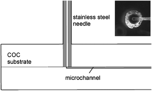 | ||
| Fig. 2 Cross-section view of needle interface (to approximate scale). Bottom view of an inserted needle is shown inset. | ||
A threaded needle interface is depicted in Fig. 3. Unlike the interference fit needle ports, the threaded needles did not generate sufficiently high stresses to produce cracking of the substrates, thus annealing was not required. Insertion of the threaded needles into the on-chip reservoirs was also easier than the interference fit needles. Because the thread pitch is known, needle seating was achieved by turning the needle by hand to within 2–3 turns of the final position, then using a microscope to gently seat the needle against the microchannel substrate. A further advantage of the threaded needles is that the threads are formed prior to chip bonding, ensuring that any debris generated during the tapping process could be removed.
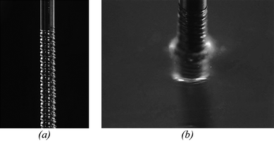 | ||
| Fig. 3 Photograph of a threaded needle port (a) before and (b) after full insertion into the chip. | ||
High pressure compatibility
Development of the needle ports was largely motivated by the need for a low dead volume interface for high performance liquid chromatography, which requires pressures on the order of 1000–5000 psi (7 to 34 MPa), well above the typical limits of adhesive-based microfluidic interfaces. The interference fit needle ports were found to provide a consistent pressure resistance of 40.9 ± 2.6 MPa (n = 10), with failure due to relative motion between the needle and chip substrate resulting in partial or complete pull-out of the needle. At pressures above 40 MPa, failure was often observed due to slippage of the capillary fitting attached to the free end of the needle. Data from these tests were ignored when evaluating average pressure resistance for the interference fit needles. The threaded needle ports resisted pressures of 40.9 ± 0.7 MPa (n = 3). In this case, failure was only observed at the capillary fitting connecting the needle with the LC pump rather than the on-chip needle port itself.Although fabrication of the threaded needle ports requires additional effort compared with the interference fit needles, they offer the benefit of being easily reusable. A set of 3 different needles sequentially inserted and removed from a threaded port 20 times showed only a slight reduction in pressure resistance to 39.0 ± 4.6 MPa, likely due to wear of the plastic threads within the COC chip. Furthermore, the threaded needles were observed to be highly robust against external torsional and bending forces, preventing damage to the ports during the formation of off-chip capillary connections.
In addition to pressure limitations imposed by the off-chip capillary fittings, it should be noted that the strength of the bond between the thermoplastic substrate layers also limits maximum operational pressure. The COC chips used in this work were bonded using a solvent bonding recipe which produces an exceptionally strong bond. However, chip failure due to delamination was occasionally observed during needle port testing at pressures ranging from 35–42 MPa. Data from these tests were discarded.
Dispersion measurements
Larger dead volumes within a fluidic path generally correlate with increased dispersion of analyte bands passing through the dead volumes. Despite their popularity as a straightforward approach to interfacing off-chip tubing with microfluidic systems, commercial Nanoports require relatively large reservoirs connecting the ports to embedded microchannels, resulting in large dead volumes, and thus a large degree of dispersion. A typical concentration profile for a dye plug injected through a Nanoport fitting is shown in Fig. 4. In addition to significant band broadening, the resulting profile also exhibits an extended tail resulting from leaking of dye from the large interfacial dead volume into the detection microchannel. As a result, sample elutes into the microchannel over a time period of over 400 s, compared with an original bandwidth of less than 20 s before reaching the Nanoport. | ||
| Fig. 4 Normalized fluorescence intensity profiles for a dye plug measured before and after injection through a commercial Nanoport interface. The on-chip measurement was performed 2 cm downstream from the interface. | ||
Injection of dye through the needle interfaces resulted in substantially less dispersion. As shown in Fig. 5, the normalized concentration profiles of dye plugs passing through 3 and 7 sequential needle port interfaces are qualitatively similar to dye plugs passing through the planar chip without the needle ports. Quantitative evaluation of dispersion within the needle interfaces was determined by measuring changes in spatial variance for the injected dye plugs. The flow rate of 0.55 µL/min was selected to allow rapid testing without introducing excessive Taylor dispersion. The hydraulic diameter d for a channel with a rectangular cross-section of height h and width w can be approximated as21
| d = 2wh/(w + h) | (1) |
| Pe = du/D | (2) |
| De = D(1 + Pe2/192) | (3) |
| σ2= 2Det | (4) |
| Point A | Point B | |
|---|---|---|
| Total path length | 8.6 cm | 18.2 cm |
| σ2theoretical/cm2 | 0.29 | 0.62 |
| σ2measured, planar/cm2 | 0.36 | 0.58 |
| σ2measured, 2-layer/cm2 | 0.44 | 1.05 |
 | ||
| Fig. 5 Normalized fluorescence intensity profiles for dye plugs before and after injection into a planar chip without needle ports, and into a 2-layer chip containing up to 7 needle port interfaces. On-chip measurements were performed at points A and B indicated in Fig. 1. | ||
Conclusion
World-to-chip interfaces for thermoplastic microfluidics employing both interference fit and threaded stainless steel hypodermic needles have been developed. From measurements of dye band dispersion, the needle ports were found to introduce minimal dead volume and dispersion within the microfluidic system. The interfaces were also compatible with operating pressures over 40 MPa, with maximum pressure limited only by chip delamination or capillary connector failure for the case of threaded needle ports.The inexpensive needle ports take advantage of the high stiffness and plastic behavior of thermoplastic polymers for their operation. In addition to enabling low dead volumes and high pressure compatibility, the ports offer several other advantages for interfacing off-chip tubing with thermoplastic microfluidics. Because adhesives are not required for sealing, the needles are fully reusable. This is particularly true for the threaded needle ports, which may be easily removed and re-inserted by hand. At the same time, potential contamination issues associated with the use of liquid epoxies and glues are avoided. The small footprint of the ports, defined by the 710 µm outer diameter of the needles, allows dense clusters of ports to be integrated into complex microfluidic systems requiring closely-spaced fluidic interfaces.
While the needle ports demonstrated here employed COC as the substrate material, this simple concept may be adapted to other thermoplastic polymers. Although not discussed in this work, we have successfully fabricated interference fit needle ports in both poly(methyl methacrylate) (PMMA) and polycarbonate (PC)23 chips. The use of threaded fittings may also find utility for elastomeric microfluidics. Similarly, alternative materials may be used for the needles themselves. For example, ports fabricated from threaded poly(etheretherketone) (PEEK) tubing have been tested, although commerically available PEEK fittings impose significant pressure limitations, and the low torsional rigidity of PEEK complicates the threading process.
Acknowledgements
This work was supported by the National Institutes of Health (R01 GM072512), and the National Science Council, Taiwan (NSC 96-2811-E-002-054).References
- C. K. Fredrickson and Z. H. Fan, Lab Chip, 2004, 4, 526–533 RSC.
- N. H. Bings, C. Wang, C. D. Skinner, C. L. Colyer, P. Thibault and D. J. Harrison, Anal. Chem., 1999, 71, 3292–3296 CrossRef CAS.
- A. Chow, in Methods in Molecular Biology, ed. C. S. Henry, Humana Press, Totowa, NJ, USA, 2006, pp. 129–143 Search PubMed.
- B. L. Gray, D. Jaeggi, N. J. Mourlas, B. P. van Drieenhuizen, K. R. Williams, N. I. Maluf and G. T. A. Kovacs, Sens. Actuators A–Phys., 1999, 77, 57–65 CrossRef.
- T. Pan, A. Baldi and B. Ziaie, J. Microelectromech. Syst., 2006, 15, 267–272 CrossRef.
- E. R. Murphy, T. Inoue, H. R. Sahoo, N. Zaborenko and K. F. Jensen, Lab Chip, 2007, 7, 1309–1314 RSC.
- E. T. Lagally, I. Medintz and R. A. Mathies, Anal. Chem., 2001, 73, 565–570 CrossRef CAS.
- V. Nittis, R. Fortt, C. H. Legge and A. J. de Mello, Lab Chip, 2001, 1, 148–152 RSC.
- A. Puntambekar and C. H. Ahn, J. Micromech. Microeng., 2002, 12, 35–40 CrossRef.
- Z. Yang and R. Maeda, J. Chromatogr. A, 2003, 1013, 29–33 CrossRef CAS.
- N. F. Yin, K. Killeen, R. Brennen, D. Sobek, M. Werlich and T. V. van de Goor, Anal. Chem., 2005, 77, 527–533 CrossRef CAS.
- R. F. Renzi, J. Stamps, B. A. Horn, S. Ferko, V. A. VanderNoot, J. A. A. West, R. Crocker, B. Wiedenman, D. Yee and J. A. Fruetel, Anal. Chem., 2005, 77, 435–441 CrossRef CAS.
- M. Brivio, R. E. Oosterbroek, W. Verboom, A. van den Berg and D. N. Reinhoudt, Lab Chip, 2005, 5, 1111–1122 RSC.
- D. Snakenborg, G. Perozziello, O. Geschke and J. P. Kutter, J. Micromech. Microeng., 2007, 17, 98–103 CrossRef.
- K. W. Oh, C. S. Park, K. Namkoong, J. Kim, K. S. Ock, S. Kim, Y. A. Kim, Y. K. Cho and C. Ko, Lab Chip, 2005, 5, 845–850 RSC.
- V. Saarela, S. Franssila, S. Tuomikoski, S. Marttila, P. Ostman, T. Sikanen, T. Kotiaho and R. Kostiainen, Sens. Actuators B–Chem., 2006, 114, 552–557 CrossRef.
- A. M. Christensen, D. A. Chang-Yen and B. K. Gale, J. Micromech. Microeng., 2005, 15, 928–934 CrossRef.
- A. A. S. Bhagat, P. Jothimuthu, A. Pais and I. Papautsky, J. Micromech. Microeng., 2007, 17, 42–49 CrossRef.
- K. W. Ro, H. Liu and D. R. Knapp, J. Chromatogr. A, 2006, 1111, 40–47 CrossRef CAS.
- D. A. Mair, E. Geiger, A. P. Pisano, J. M. J. Frechet and F. Svec, Lab Chip, 2006, 6, 1346–1354 RSC.
- D. Di Carlo, D. Irimia, R. G. Tompkins and M. Toner, Proc. Natl. Acad. Sci. USA, 2007, 104, 18892–18897 CrossRef CAS.
- S. A. Rani, B. Pitts and P. S. Stewart, Antimicrobial Agents and Chemotherapy, 2005, 49, 728–732 CrossRef CAS.
- L. P. Hromada, B. J. Nablo, J. J. Kasianowicz, M. A. Gaitan and D. L. DeVoe, Lab Chip, 2008, 8, 602–608 RSC.
| This journal is © The Royal Society of Chemistry 2009 |