Ir(ppy)3 phosphorescent microrods and nanowires: promising micro-phosphors†
Hao
Wang
ab,
Qing
Liao
a,
Hongbing
Fu
*a,
Yi
Zeng
ab,
Ziwen
Jiang
ab,
Jinshi
Ma
a and
Jiannian
Yao
*a
aBeijing National Laboratory for Molecular Sciences (BNLMS), Key Laboratory of Photochemistry, Institute of Chemistry, Chinese Academy of Sciences, Zhongguancun, Beijing, 100190, P. R. China. E-mail: jnyao@iccas.ac.cn; hongbing.fu@iccas.ac.cn; Fax: +86-10-82616517; Tel: +86-10-82616517
bGraduate University of Chinese Academy of Sciences (GUCAS), Beijing, 100049, P. R. China
First published on 10th November 2008
Abstract
We prepared crystalline Ir(ppy)3 microrods through a facile self-assembly growth method by employing the so-called reprecipitation technique, and Ir(ppy)3 nanowires by a solvent-evaporation route. Both have lengths up to several tens of micrometer, but possess significantly different diameters: 1 µm for microrods and 100 nm for nanowires. The electron diffraction (ED) and X-ray diffraction (XRD) results clarify that both microrods and nanowires preferentially grow along the crystal [001] direction. However, the former have a regular hexagonal geometry and single crystalline in nature, while the latter are polycrystalline with a round cross section. Remarkably, microrods and nanowires of Ir(ppy)3 present distinct optical properties. The phosphorescence decay of Ir(ppy)3 microrods and nanowires is much faster than that in degassed solution and polymethylmethacrylate (PMMA) film. The phosphorescence green color of microrods is similar to that of Ir(ppy)3 molecules doped in PMMA films, while nanowires actually emit yellow light probably from the low-energy trap as a result of its polycrystalline nature. Furthermore, the transverse nanoscale and longitudinal microscale dimensions and well-defined faceting nature of microrods enable the observation of evident optical waveguiding. No optically pumped lasing is observed because of intense triplet–triplet exciton annihilation. Our results afford a novel strategy of phosphorescence emission color tuning by controlling the nano- to microstructure dimensions. The microrod phosphorescence waveguides may be used as building blocks for future miniaturized photonic devices.
Introduction
In recent years, organic nano- to micrometer-sized architectures have been attracting considerable research interest due to their potential applications in fields of optoelectronics,1,4 nonlinear optics,5 and photonics.6 Presently, ever increasing efforts have been made for controlling the morphology of organic functional nanomaterials, as the optical, electronic, and chemical properties of these molecular assemblies can be modulated by their size1–3 and shape.4 For example, one-dimensional nanostructures facilitate the construction of optical waveguides, which are capable of propagating light efficiently on the subwavelength scale, and therefore serve as the key module of future miniaturized optoelectronic circuits. However, extensive studies in this field are focused on inorganic materials,7 while few low molecular-weight organic compounds are used to construct optical waveguides.8 As compared with inorganic materials, organic ones offer several intrinsic advantages such as high fluorescence efficiency and superior control over the wavelength of light emitted by careful design of the molecules. Very recently Redmond et al. reported waveguiding effects and optically pumped lasing in single conjugated polymer (poly(9,9-dioctylfluorene)) based nanowires.9 Moreover, our group demonstrated that nanowire waveguides and lasers can also be extended to small organic molecules.10 Both cases used high fluorescence compounds. To the best of our knowledge, fabrication of optical waveguides from phosphorescent molecules remains still a challenge.Iridium organometallic complexes, due to the large amount of spin–orbit coupling induced by the heavy metal ion, are good organic phosphorescent materials.11 Recently, they became particularly attractive due to their very high efficiency of electrophosphorescence in organic light emitting devices (OLEDs).12,13 The phosphorescence color of fac-tris(2-phenylpyridine) iridium (Ir(ppy)3) (λmax = 515 nm) accords with the Commission Internationale de l'Éclairage (CIE) coordinates for green color. It has been proved that the triplet metal-to-ligand charge transfer state (3MLCT) is the lowest-lying emissive state.14–16 Due to the importance of fac-Ir(ppy)3 for green light-emitting OLEDs, it is of interest to study the preparation and optical properties of crystalline Ir(ppy)3 with regular nanostructures or microstructures. Herein, we prepared crystalline Ir(ppy)3 microrods through a facile self-assembly growth method by employing the so-called reprecipitation technique,17 and Ir(ppy)3 nanowires by a solvent-evaporation route. Both have lengths up to several tens of micrometer, but possess significantly different diameters: 1 µm for microrods and 100 nm for nanowires. The electron diffraction (ED) and X-ray diffraction (XRD) results clarify that both microrods and nanowires preferentially grow along the crystal [001] direction. However, the former have a regular hexagonal geometry18 and are single crystalline in nature, while the latter are polycrystalline with a round cross section. Remarkably, microrods and nanowires of Ir(ppy)3 exhibit distinct optical properties. The phosphorescence decay of Ir(ppy)3 microrods and nanowires is much faster than that in degassed solution and polymethylmethacrylate (PMMA) film. The phosphorescence green color of microrods is similar to that of Ir(ppy)3 molecules doped in PMMA film, while nanowires actually emit yellow light probably from the low-energy trap as a result of its polycrystalline nature. Furthermore, the transverse nanoscale and longitudinal microscale dimensions and well-defined faceting nature of microrods enable the observation of evident optical waveguiding. No optically pumped lasing is observed because of intense triplet–triplet exciton annihilation. Our results afford a novel strategy of phosphorescence emission color tuning by controlling the nano- to microstructure dimensions. The microrod phosphorescence waveguide may be used as building blocks for future miniaturized photonic devices.
Experimental
A. Materials
The organometallic complex fac-Ir(ppy)3 was purchased from Beijing Elight Optoelectronic Material Technology Co., China. PMMA was purchased from Aldrich Co., Germany. The solvents 1,4-dioxane, acetonitrile, alcohol, dichloromethane and toluene were purchased from Beijing Chemical Co., China. All compounds were used as supplied without further purification.The Ir(ppy)3/PMMA films were prepared by spin-coating the appropriate solutions on optical glass substrates. Both the solutions and the substrates are at room temperature for the spin coating. The films containing 4 wt% Ir(ppy)3 in PMMA are prepared by dissolving 2 mg Ir(ppy)3 and 50 mg PMMA in 5 ml dichloromethane, and spin-coating the solution on the substrate at a speed of 1800 rpm. The degassed toluene solution was prepared after de-aeration by argon bubbling for 1 h.
The as-prepared Ir(ppy)3 microrod and nanowire samples were prepared by depositing the solution containing the fibers onto a glass substrate (microscope cover glass, 20 mm × 20 mm). The samples were dried under ambient conditions in order to evaporate the solvent.
B. Preparation
Ir(ppy)3 microrods were prepared by a facile reprecipitation method17 under ambient conditions. Briefly, a stock solution containing 1 mmol L−1 Ir(ppy)3 in a mixed solvent of 1,4-dioxane and acetonitrile (1:1, v/v) was prepared. Then, 100 µL of this stock Ir(ppy)3 solution was quickly injected into 2 mL of ethanol without stirring. The mixed solvent is a good solvent but ethanol is a poor one for Ir(ppy)3, so aggregation of Ir(ppy)3 occurred as a consequence of the change in the solvent quality. Then, the sample was left undisturbed for about 2 hours to stabilize the microstructures.Ir(ppy)3 nanowires were prepared by facile solvent evaporation on a horizontal silicon substrate. In a typical experiment, a drop of Ir(ppy)3 solution (1 mmol L−1 Ir(ppy)3 in 1,4-dioxane and acetonitrile (1:1, v/v)) was placed on a silicon substrate under ambient conditions. After complete evaporation of solvent, Ir(ppy)3 nanowires was formed on the substrate.
C. Measurements
The morphologies and sizes of the as-prepared Ir(ppy)3 microrods and nanowires were characterized by field emission scanning electron microscopy (FE-SEM, Hitachi S-4300) at an accelerating voltage of 15 kV. To minimize sample charging, a thin layer of Pt was deposited onto the samples before SEM examination. The sample was then observed with a Philips Tecnai F30 transmission electron microscope (TEM) operated at an accelerating voltage of 200 kV. They were also characterized by X-ray diffraction (XRD, Japan Rigaku D/max-2500) with Cu Kα radiation, and fluorescence microscopy (Olympus IX71). Microarea PL microscopy images of single microrods were obtained by near-field scanning optical microscopy (NSOM). For the collection of photoluminescence (PL) spectra, single microrods and nanowires were excited with a continuous He-Cd laser (λ = 442 nm). PL spectra were then collected using an objective coupled into an optical fiber and a liquid nitrogen cooled charge-coupled device (CCD).The stationary UV-visible absorption spectra of the Ir(ppy)3 solution were measured on a Perkin-Elmer Lambda 35 spectrometer with a scanning speed of 480 nm/min and a slit width of 1 nm. The stationary fluorescence spectra were recorded on a Hitachi F-4500 fluorescence spectrophotometer using a right angle configuration. Slits were set to provide widths of 5 nm for both the excitation and the emission monochromators. Cuvettes with a 1 cm path length were used. All spectroscopic measurements were carried out at room temperature.
PL kinetics were measured using a time-resolved fluorescence spectrometer, which has been described in detail elsewhere.19 Briefly, the 800 nm laser pulses generated from a Ti:sapphire regenerative amplifier (Spitfire, Spectra Physics) were frequency doubled and used as the excitation pulses. The excitation pulse energy was ∼100 nJ/pulse at a pulse repetition rate of 1 kHz which was focused onto a spot 0.5 mm in diameter. Photoluminescence collected with the 90 degree geometry was dispersed by a polychromator (250is, Chromex) and collected with a photon-counting type streak camera (C5680, Hamamatsu Photonics). The data detected by digital camera (C4742-95, Hamamatsu) were routinely transferred to PC for analysis with HPDTA software. The spectral resolution was 2 nm, and the temporal resolution was 2–100 ps depending on the delay-time-range setting. All the spectroscopic measurements were carried out at room temperature.
Results and discussion
A. Characterization
Ir(ppy)3 microrods were prepared as described before. The microrods were very uniform in size, as indicated by FE-SEM. Fig. 1(A) shows a low-magnification SEM image of the sample. It can be obviously seen that rod-shaped microstructures have been successfully prepared on a large scale. The rather straight microrods have a length of ∼80 µm and width of ∼1 µm, and have a uniform size along the entire length for each microrods. In addition, the surfaces of the microrods are clean and smooth. The high-magnification SEM images (Fig. 1(C) and (D)) of some microrods growing out of the substrate surface indicate that the microrods have highly regular hexagonal prism geometric shapes and smooth end surfaces. Each microrod has a hexagonal cross-section and six regular facets. The morphology of the microrods was further confirmed by TEM (Fig. 1(B)), which shows that the uniform Ir(ppy)3 structures are solid microrods of micrometer diameter. The microrods are single-crystalline rather than polycrystalline, as revealed by the sharp spots in the corresponding selected area electron diffraction (SAED) patterns (the inset of Fig. 1(B) is a typical example). The energy dispersive X-ray (EDX) spectrum (ESI† Fig. S1) of the microrod shows obvious peaks of the elements C, N and Ir which constitute the Ir(ppy)3 molecules (C33H24IrN3). The peak of Si arises from the Si grid for SEM characterization. The presence of O comes mainly from atmospheric contamination due to exposure of the sample to air. Therefore, the result implies the prepared microrods are composed of Ir(ppy)3 molecules.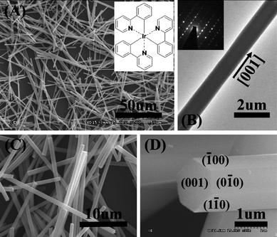 | ||
| Fig. 1 Low (A) and high (C, D) magnification SEM images, and TEM image (B) of Ir(ppy)3 microrods. The inset of image (A) shows the chemical structure of fac-Ir(ppy)3. The inset of image (B) is the corresponding SAED pattern of Ir(ppy)3 microrods. | ||
We prepared the Ir(ppy)3 nanowires by solvent evaporation on a silicon substrate. After complete evaporation of solvent, the substrate was examined by FE-SEM. As shown in Fig. 2(A) and (C), many nanowires were deposited on the substrate. The majority of the nanowires had a length of several mm and a diameter of ∼100 nm. As shown in Fig. 2(B), the cross section of the nanowires is round. The morphology of the nanowires was further confirmed by TEM (Fig. 2(D)), which shows that the Ir(ppy)3 uniform structures are solid nanowires. The nanowires are not very single crystalline, because few sharp spots can be seen in the corresponding SAED pattern.
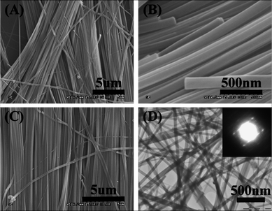 | ||
| Fig. 2 Low (A) and high (B, C) magnification SEM images, and TEM image (D) of Ir(ppy)3 nanowires. The inset of image (D) is the corresponding SAED pattern of Ir(ppy)3 nanowires. | ||
XRD experiments were performed to further investigate the crystal structure of the Ir(ppy)3 microrods and nanowires. The comparison between the XRD profiles of Ir(ppy)3 microrods, nanowires and the simulated powder pattern in Fig. 3 provides a clue for us to understand the real picture of molecular packing at the microscale regime. The simulated powder pattern of fac-Ir(ppy)3 was obtained by using of the program MERCURY based on the single-crystal structure data reported by Breu and co-workers.20 It can be seen that the diffraction peaks observed for microrods and nanowires can be perfectly indexed to the single-crystal data, confirming the microstructures consisted of pure Ir(ppy)3 and the starting Ir(ppy)3 molecules were self-assembled into a well-defined 1D microstructure. For Ir(ppy)3 hexagonal microrods, a distinct strong peak corresponding to the (2−10) plane is clearly observed in the diffraction profile, which reveals that perfect crystal packing is formed. In contrast to the case of the microrods, there are broadened diffraction peaks detectable for nanowires indicating poor crystal packing. The peak corresponding to (2−10) plane is also clearly observed in the diffraction profile of nanowires. The peaks corresponding to (3−2−2), (4−20), and (302) planes become a broadened band. After the determination of the crystal structure of the microrods, the SAED pattern in Fig. 1(B) could be easily indexed according to the interplanar spacing of fac-Ir(ppy)3. The result reveals that the Ir(ppy)3 molecules within the hexagonal microrods prefer to arrange themselves along the crystal [001] direction, that is, the crystallographic c axis direction. Then, we can label the end face of the microrod with (001) plane in Fig. 1(D). The six side faces of the hexagonal microrods are equivalent. Three equivalent planes are labeled in Fig. 1(D). In addition, due to the relatively strong peak corresponding to the (2−10) plane in the diffraction profile of nanowires, we think the Ir(ppy)3 molecules within the round nanowires also prefer to arrange themselves along the crystal [001] direction. The nanowires are soft without any pointedness compared with the microrods which have highly regular hexagonal prism geometric shape. Maybe the broadened diffraction peak in the diffraction profile of nanowires is owing to the crystal defects, and these defects disturb the presence of high Miller index surfaces.
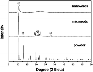 | ||
| Fig. 3 XRD patterns of Ir(ppy)3 nanowires (above), microrods (middle) and simulated powder pattern (below) from the published crystal structure data of fac-Ir(ppy)3. | ||
B. Spectra
The absorption and emission spectroscopic behaviour of fac-Ir(ppy)3 were studied at room temperature. Liquid solution, doped film, a single microrod and a single nanowire were investigated. There is very little overlap between the absorption and emission spectra of liquid solution. The absorption spectrum of Ir(ppy)3 dichloromethane solution is nearly the same as that for Ir(ppy)3 in solution as reported previously.21 Clear evidence for significant mixing of the singlet and triplet excited states is seen in both the absorption and emission spectra of these complexes. Ir(ppy)3 shows intense absorption from ligand π–π* and MLCT transitions. The absorption spectrum is shown in Fig. 4. The π–π* absorption (singlet–singlet ligand-centered, 1LC) band for Ir(ppy)3 falls in the range 250–320 nm which is an intense ultraviolet band, and closely resembles the spectrum of the free ppy ligand. In turn, the weaker absorption band (320–510 nm) of low energy that extend to the visible region is conventionally assigned to metal-to-ligand charge-transfer transitions (MLCT).22 Both 1MLCT and 3MLCT bands are typically observed. The high degree of spin–orbit coupling is evident in comparing the oscillator strengths for the two MLCT bands. More intense features with a main maximum at 385 nm are conventionally assigned to 1MLCT transitions, and weak broad shoulders in the longer wavelength range (450–510 nm) are ascribed to the 3MLCT transitions and their vibrational satellites. The formally spin-forbidden 3MLCT transitions acquire intensity by effective mixing with higher energy spin-allowed transitions due to the strong spin–orbit coupling of iridium atoms.23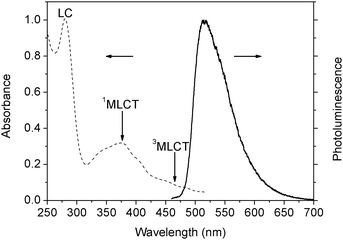 | ||
| Fig. 4 Normalized absorption (dashed line) and photoluminescence (solid line) spectra of Ir(ppy)3 dissolved in dichloromethane (10−5 mol L−1). | ||
The photoluminescence spectrum of Ir(ppy)3 dichloromethane solution at room temperature consists of a broad, featureless and asymmetric band with its intensity maximum at 515 nm, which is nearly the same as that for Ir(ppy)3 in solution as previously measured in various solvents.22,24Fig. 4 shows the photoluminescence spectrum of Ir(ppy)3 dichloromethane solution observed at room temperature which has one major peak. According to the previous works, the observed PL emission is commonly identified as phosphorescence from the 3MLCT state. This assignment was based upon PL lifetime measurements,24 quantum chemical calculations25 and extensive experimental works.13,22,26,27 A number of studies confirm that Ir(ppy)3 MLCT singlet excitons convert to the triplet excited states with nearly 100% conversion of intersystem crossing (ISC) which is consistent with the recent femtosecond luminescence and transient absorption study22d,28 and quantum mechanical calculations indicating that there exists a high density of these spin-mixed states (about 70 states in the lowest 1 eV).25c
A vibronic progression is seen in the phosphorescence band for Ir(ppy)3 doped in 4,4′-N,N′-dicarbazole-biphenyl (CBP).29 Tsuboi and Aljaroudi obtained good agreement between the observed and calculated line shapes using the Gaussian model. In turn, we try to calculate line shapes of Ir(ppy)3 spectra using the Gaussian model. In the PL spectrum of Ir(ppy)3 liquid solution (ESI† Fig. S2), the peaks at 508, 533, and 567 nm are attributed to the calculated zero (0–0), one (0–1), and two (0–2) phonon bands, respectively.29 The 0–0 transition at 508 nm is slightly lower in energy than the calculated vertical transition energy of MLCT (at 2.59 eV, 479 nm) between the lowest triplet state and the ground state,25a which can be explained by structural relaxation in excited state and solvation.21b The shape of the PL spectrum in liquid solution is independent of the excitation wavelength in the range of 350–480 nm. The PL spectra of a single microrod, a single nanowire and Ir(ppy)3 doped in a PMMA film are shown in Fig. 5. The spectral shapes of the PL spectra in PMMA film and liquid solution are similar. A vibronic structure is resolved. The PL spectrum of Ir(ppy)3 doped in PMMA has a shoulder at the low energy side (at about 535 nm) of the main band (at about 510 nm) as shown in Fig. 5A. The main band and shoulder are respectively attributed to the 0–0 and 0–1 vibronic lines. The PL spectrum of a single microrod (Fig. 5B) is structured, and its maximum (538 nm) is substantially red-shifted in comparison to the solution and the PMMA film. For a single nanowire (Fig. 5C) the PL spectrum is very broadened and structured. Intermolecular interactions are responsible for the red shift of the solid state PL spectrum. In addition, we calculated line shapes of the spectrum of a single rod, a single wire and Ir(ppy)3 doped in PMMA film. The calculated peaks' information is seen in the insets of Fig. 5. We find that the peak centers of PMMA film and single rod are nearly the same; the 0–1 and 0–2 bands of a single rod are stronger than those of PMMA film. Maybe aggregation increases population distributions of these bands. In particular, there are 3 peaks included in the very broadened spectrum of the single wire and the peak centers of the single wire are red-shifted diversely. The peak of the 0–1 band moves to 553 nm and the peak of the 0–2 band moves to 616 nm with a ∼40 nm red-shift. The population distributions of the 0–2 band are increased and the 0–0 band nearly disappeared. The crystal defects and relatively small diameter of the nanowire may lead to the very broadened spectrum and the increase of the 0–2 band.
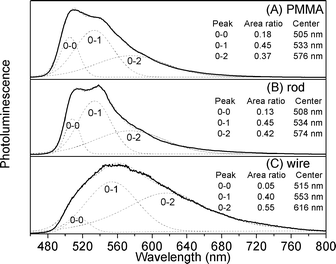 | ||
| Fig. 5 Normalized PL spectra of Ir(ppy)3 in PMMA film (A), a single microrod (B) and a single nanowire (C), excited by a continuous He-Cd laser (λ = 442 nm). Measured and calculated (dashed line) PL spectra are shown. The sum spectrum was obtained by summation of the calculated zero (0–0), one (0–1), and two (0–2) phonon bands. | ||
The solid state effect on PL of a single microrod and a single nanowire appears mainly in considerable reduction of the PL quantum efficiency and additional inhomogeneous broadening of the PL spectrum.21b,22e Compared with measurements in dilute solutions where nearly a single decay time of 1–2 µs is reported,21b,24a,30 the PL decay of Ir(ppy)3 microrods and nanowires turned out to be rather faster and non-monoexponential,21b,31 which indicates additional non-radiative decay channels caused by aggregation in the solid state. There occurs a strong self-quenching.
The PL signal decay curves for Ir(ppy)3 microrods and nanowires are shown in Fig. 6. In the air saturated liquid solution (ESI† Fig. S3A) and in the degassed toluene solution (ESI† Fig. S3B) monoexponential PL decays are observed. Ir(ppy)3 is sensitive to dissolved oxygen and the luminescence is quenched substantially in nondegassed solution. In degassed solution, the PL signal decay is independent of the wavelength in the range of 500–600 nm and dominated by a long ∼1.16 µs component. The PL lifetime in the nondegassed solution decreases dramatically to ∼38.6 ns. The long lifetime of the PL and quenching by oxygen are signatures of phosphorescence. We, therefore, can safely assign the green emission with a maximum at 515 nm to the radiative decay of the triplet state 3MLCT to the ground state. In PMMA film, the PL decay (ESI† Fig. S3C) is also monoexponential, with a lifetime of ∼1.18 µs. The PL decay in Ir(ppy)3 nanowires (Fig. 6) is much faster than that in solution and PMMA film, which indicates that additional nonradiative decay channels of the emissive triplet state prevail in Ir(ppy)3 nanowires. A fast-decay component of ∼0.7 ns, with a relative amplitude of 0.56, is observed in the Ir(ppy)3 nanowires, along with a ∼3.58 ns component (with a relative amplitude of 0.44). The PL decay in Ir(ppy)3 microrods is slower than in the Ir(ppy)3 nanowires; however, it is still faster than that in degassed solution and PMMA film, indicating that quenching of the emissive state also occurs in Ir(ppy)3 microrods. A fast-decay component of ∼4.09 ns, with a relative amplitude of 0.20, is observed in the Ir(ppy)3 microrods, along with a dominant 34.7 ns component (with a relative amplitude of 0.80). The fast components of the PL decays are due to the transfer of excitation to the quenching sites.
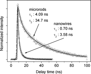 | ||
| Fig. 6 The PL signal decay curves for Ir(ppy)3 microrods and nanowires. | ||
For Ir(ppy)3 microrods and nanowires, non-monoexponential PL decay is observed because the picosecond pulse excitation leads to nearby excitation of triplet molecules quenching by triplet–triplet annihilation. In addition, rapid energy transfer between excited molecules and neighbouring unexcited molecules is likely to bring two nearby excited molecules together for triplet–triplet annihilation. The dynamics of triplet–triplet annihilation in organometallic compounds were described in detail by Forrest and co-workers.33 An excitation intensity dependence of the PL lifetimes is observed for Ir(ppy)3 microrods and nanowires, as shown in Table 1. The lifetime is observed to decrease with increasing excitation intensity. The excitation intensity dependence of the PL lifetimes was also observed by Forrest and co-workers.32 At a later time, they demonstrated that the observed phenomenon was principally due to triplet–triplet annihilation.33 It is also suggested that triplet–triplet annihilation occurs in Ir(ppy)3 microrods and nanowires.
| Sample | τ1 (ns) a | A1a | τ2 (ns) a | A2a |
|---|---|---|---|---|
| a The decay kinetics were fitted by a sum of exponential functions: I(t) = A1 exp(−t/τ1) + A2 exp(−t/τ2), where the A and τ terms represent the pre-exponential factors and time constants, respectively. | ||||
| Microrods 1.4 µJ/pulse | 3.58 | 0.60 | 33.96 | 0.40 |
| Microrods 7.6 µJ/pulse | 3.21 | 0.76 | 25.23 | 0.24 |
| Microrods 18.9 µJ/pulse | 2.78 | 0.81 | 21.52 | 0.19 |
| Microrods 25.1 µJ/pulse | 2.65 | 0.86 | 20.78 | 0.14 |
| Nanowires 1.5 µJ/pulse | 0.69 | 0.67 | 3.36 | 0.33 |
| Nanowires 7.4 µJ/pulse | 1.34 | 1.00 | ||
| Nanowires 18.8 µJ/pulse | 1.09 | 1.00 | ||
| Nanowires 26.0 µJ/pulse | 0.86 | 1.00 |
As Breu and coworkers reported,20rearrangements of molecular packing and the existence of many distorted regions at thin lamellar domain interfaces stacked along the c axis profoundly affects the photophysical properties of Ir(ppy)3. This inherent intrinsic disorder is not only a reason for the nonlinear second order activity of nominally centrosymmetric Ir(ppy)3 crystals, but also has a pronounced effect on PL spectra. The PL spectrum of Ir(ppy)3 nanowires is very broadened and red-shifted; simultaneously considering the PL lifetime, it is dominated by a different excited species, which does not appear in microrods and solution emission. This type of behavior is expected when excitation is transferred to sites with a lower optical gap in Ir(ppy)3 nanowires. The existence of energy traps such as crystal defects in Ir(ppy)3 nanowires is proposed to be responsible for the observed quenching effects. When excitation is transferred to one of these crystal defects during migration, its energy is reduced by the interaction energy and these sites act as excitation traps. Consequently, poor crystal packing may be the main reason for the relatively short PL lifetime and distinctive spectrum.
C. Waveguides
PL microscopy images of Ir(ppy)3 microrods and nanowires on quartz substrates are shown in Fig. 7. A characteristic green emission for Ir(ppy)3 is emitted from the microrods, with intense luminescence spots observed at both ends of each microrod and a weaker emission observed from the rod bodies. This is a typical feature of an optical waveguide and it suggests that the microrods are able to absorb the excitation light and propagate the PL emission towards the tips.8,34 Almost all of the Ir(ppy)3 microrods which were analysed exhibited this kind of waveguide behavior. Additionally, bright emission spots can be observed at the intersections of crossed rods as well as at the tips, which was also seen in our previous work.10 This suggests that the emitted light can also be propagated from one rod to another. In contrast, the Ir(ppy)3 nanowires exhibit a green-yellow emission which is in agreement with the broadened emission spectrum of the nanowires. Bright luminescence spots cannot be observed at both ends of each wire and luminescence can be observed along the wire bodies. This means the nanowires do not have the features of an optical waveguide and it suggests that the nanowires cannot effectively propagate the PL emission towards the tips.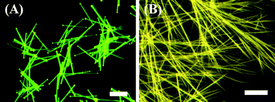 | ||
| Fig. 7 PL microscopy images of Ir(ppy)3 microrods (A) and nanowires (B) deposited on a glass substrate. Scale bar is 50 µm. | ||
Microarea PL microscopy images of single rods were obtained by near-field scanning optical microscopy (NSOM). Microrods were excited with a focused laser (442 nm) down to the diffraction limit at different local positions relative to a NSOM collection tip that was held stationary over one of their ends. With this technique, the process of light traveling along the microrods can be investigated effectively by moving the excitation laser. Fig. 8 shows that the local light emission of single microrod upon laser excitation was so strong that it was imaged clearly using a color charge-coupled device (CCD). Interestingly, the microrods exhibit excellent waveguide properties and the guided PL is emitted from both tips irrespective of the excitation position (Fig. 9A), whereas generally in micro-area PL images the light emission can only be observed locally at the area of excitation. The localization of the outcoupling of the light at the ends of each microrod is a typical characteristic of strong waveguiding behavior. Since the waveguided light is generated from PL within the microrods these rods can be classified as active waveguides,9b as compared to passive ones where light must be coupled-in from external sources.35
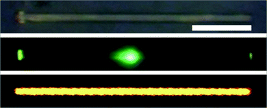 | ||
| Fig. 8 Bright-field image (above), dark-field image (middle) and confocal image (below) of a single Ir(ppy)3 microrod. Scale bar is 20 µm. | ||
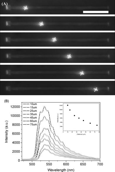 | ||
| Fig. 9 (A) PL images were collected upon excitation of identical microrods at six different positions (indicated by cross frames). Scale bar is 20 µm. (B) Spatially resolved PL spectra of the waveguided emission that is outcoupled at the tip of a single microrod for different separation distances (between the excitation spot and the rod tip). Inset shows peak intensity at maximum versus excitation position for the PL spectra. | ||
The spatially resolved spectra of the waveguided emission that is outcoupled at a microrod tip as a function of different propagation distances (between the excitation spot and the rod tip) is shown in Fig. 9B. The vibrational fine structures can be observed from the outcoupled waveguided emissions. Shorter wavelengths gradually disappear with increasing propagation distances between vibrational structures.10a Then, due to the fade-out of shorter wavelengths, lower energy vibrational peaks become more predominant. This can be ascribed to the re-absorption of waveguided light during the propagation of PL along the microrod. Moreover, the tip emission intensity obviously decreases across all emission wavelengths upon an increase in propagation distance. The distance dependence of intensity, shown in Fig. 9B inset, indicates that the intensity of the outcoupled light decreases almost exponentially with the increase in propagation distance, which is a typical characteristic of active waveguides.
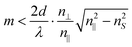
It has been demonstrated8 that light in such a waveguide can only propagate within the transverse magnetic (TM) modes, whereby the number of possible modes, m, is restricted by
 | (1) |
On the basis of the experimental results discussed above, relatively large width of microrods may result in excellent waveguide properties. This provides useful information for the construction of microscale photonic devices from molecular materials. This result will enable scientists to explore novel applications in the field of photonic devices.
Conclusions
In the study presented in this paper, we synthesize Ir(ppy)3 microrods with regular hexagonal shape and good crystallinity via a facile self-assembly route. A solvent-evaporation route is used to synthesize Ir(ppy)3 nanowires. The emission spectroscopic behaviour of Ir(ppy)3 microrods and nanowires is investigated. The PL spectrum of Ir(ppy)3 microrods is structured, and its maximum (538 nm) is substantially red-shifted, in comparison to those of the solution and the PMMA film. Intermolecular interactions are responsible for the red-shift of the solid state PL spectrum. For the nanowires the PL spectrum is very broadened and structured. The crystal defects and relatively small diameter of the nanowire may lead to such a broadened spectrum. The Ir(ppy)3 microrods exhibit a green emission. In contrast, the Ir(ppy)3 nanowires exhibit a green-yellow emission which is in agreement with the broadened emission spectrum of the nanowires. This affords a novel strategy of emission color tuning by controlling the morphology. The PL decay of Ir(ppy)3 microrods and nanowires is much faster than that in solution and PMMA film. Combine with the excitation intensity dependence of the PL lifetimes, it is suggested that triplet–triplet annihilation occurs in Ir(ppy)3 microrods and nanowires. This annihilation may affect the OLED performance in nanosecond pulse applications.Relatively large width of microrods results in excellent waveguide properties. We also demonstrate that as-prepared single crystalline microrods behave as microscale active phosphorescence waveguides. No optically pumped lasing is observed because of intense triplet–triplet exciton annihilation. Such phosphorescence waveguides may be used as building blocks for microscale photonic devices. The results presented in this paper provide useful information for the design and fabrication of microscale photonic devices from molecular materials. This will enable scientists to explore novel applications in the field of photonic devices.
Acknowledgements
This work was supported by the National Natural Science Foundation of China (Nos. 90301010, 20373077, 90606004), the Chinese Academy of Sciences (“100 Talents” program), and the National Research Fund for Fundamental Key Project 973 (2006CB806200).References
-
(a) B. K. An, S. K. Kwon, S. D. Jung and S. Y. Park, J. Am. Chem. Soc., 2002, 124, 14410 CrossRef CAS
; (b) S. J. Lim, B. K. An, S. D. Jung, M. A. Chung and S. Y. Park, Angew. Chem., Int. Ed., 2004, 43, 6346 CrossRef CAS
-
(a) F. Bertorelle, D. Lavabre and S. Fery-Forgues, J. Am. Chem. Soc., 2003, 125, 6244 CrossRef CAS
-
(a) H. B. Fu and J. N. Yao, J. Am. Chem. Soc., 2001, 123, 1434 CrossRef CAS
-
(a) K. Balakrishnan, A. Datar, R. Oitker, H. Chen, J. Zuo and L. Zang, J. Am. Chem. Soc., 2005, 127, 10496 CrossRef CAS
-
(a) S. Kim, Q. D. Zheng, G. S. He, D. J. Bharali, H. E. Pudavar, A. Baev and P. N. Prasad, Adv. Funct. Mater., 2006, 16, 2317 CrossRef CAS
-
(a) A. D. Peng, D. B. Xiao, Y. Ma, W. S. Yang and J. N. Yao, Adv. Mater., 2005, 17, 2070 CrossRef CAS
-
(a) P. Yang, H. Yan, S. Mao, R. Russo, J. Johnson, R. Saykally, N. Morris, J. Pham, R. He and H. J. Choi, Adv. Funct. Mater., 2002, 12, 323 CrossRef CAS
-
(a) K. Takazawa, Y. Kitahama, Y. Kimura and G. Kido, Nano Lett., 2005, 5, 1293 CrossRef CAS
-
(a) D. O'Carroll, I. Lieberwirth and G. Redmond, Nat. Nanotechnol., 2007, 2, 180 Search PubMed
- Y. S. Zhao, A. D. Peng, H. B. Fu, Y. Ma and J. N. Yao, Adv. Mater., 2008, 20, 1661 CrossRef CAS
-
(a) M. A. Baldo, M. E. Thompson and S. R. Forrest, Nature, 2000, 403, 750 CrossRef CAS
-
(a) M. A. Baldo, M. E. Thompson and S. R. Forrest, Pure Appl. Chem., 1999, 71, 2095 CrossRef CAS
-
(a) C. Adachi, M. A. Baldo, M. E. Thompson and S. R. Forrest, J. Appl. Phys., 2001, 90, 5048 CrossRef CAS
- W. J. Finkenzeller and H. Yersin, Chem. Phys. Lett., 2003, 377, 299 CrossRef CAS
- W. Holzer, A. Penzkofer and T. Tsuboi, Chem. Phys., 2005, 308, 93 CrossRef CAS
- K. Goushi, Y. Kawamura, H. Sasabe and C. Adachi, Jpn. J. Appl. Phys., 2004, 43, L937 CrossRef CAS
-
(a) H. Kasai, H. S. Nalwa, H. Oikawa, S. Okada, H. Matsuda, N. Minami, A. Kakuta, K. Ono, A. Mukoh and H. Nakanishi, Jpn. J. Appl. Phys., 1992, 31, L1132 CAS
- J. S. Hu, H. X. Ji, A. M. Cao, Z. X. Huang, Y. Zhang, L. J. Wan, A. D. Xia, D. P. Yu, X. M. Meng and S. T. Lee, Chem. Commun., 2007, 3083 RSC
- Y. S. Wu, J. Li, X. C. Ai, L. M. Fu, J. P. Zhang, Y. Q. Fu, J. J. Zhou, L. Li and Z. S. Bo, J. Phys. Chem. A, 2007, 111, 11473 CrossRef CAS
- J. Breu, P. Stössel, S. Schrader, A. Starukhin, W. J. Finkenzeller and H. Yersin, Chem. Mater., 2005, 17, 1745 CrossRef CAS
-
(a) W. Stampor, J. Mężyk and J. Kalinowski, Chem. Phys., 2004, 300, 189 CrossRef CAS
-
(a) S. Lamansky, P. I. Djurovich, D. Murphy, F. Abdel-Razzaq, H. E. Lee, C. Adachi, P. E. Burrows, S. R. Forrest and M. E. Thompson, J. Am. Chem. Soc., 2001, 123, 4304 CrossRef CAS
- M. G. Colombo, A. Hauser and H. U. Güdel, Top. Curr. Chem., 1994, 171, 143 CAS
-
(a) K. A. King, P. J. Spellane and R. J. Watts, J. Am. Chem. Soc., 1985, 107, 1431 CrossRef CAS
-
(a) P. J. Hay, J. Phys. Chem. A, 2002, 106, 1634 CrossRef CAS
-
(a) W. Finkenzeller, P. Stössel, M. Kulikova and H. Yersin, SPIE Proc., 2004, 5214, 356
- S. Kodate and I. Suzuka, Jpn. J. Appl. Phys., 2006, 45, 574 CrossRef CAS
- G. J. Hedley, A. Ruseckas and I. D. W. Samuel, Chem. Phys. Lett., 2008, 450, 292 CrossRef CAS
- T. Tsuboi and N. Aljaroudi, Jpn. J. Appl. Phys., 2008, 47, 1266 CrossRef CAS
- K. Dedeian, P. I. Djurovich, F. O. Garces, G. Carlson and R. J. Watts, Inorg. Chem., 1991, 30, 1687 CrossRef CAS
- C. Adachi, M. A. Baldo, S. R. Forrest and M. E. Thompson, Appl. Phys. Lett., 2000, 77, 904 CrossRef CAS
- M. A. Baldo, D. F. O'Brien, Y. You, A. Shoustikov, S. Sibley, M. E. Thompson and S. R. Forrest, Nature, 1998, 395, 151 CrossRef CAS
- M. A. Baldo, C. Adachi and S. R. Forrest, Phys. Rev. B, 2000, 62, 10967 CrossRef CAS
-
(a) H.-J. Chio, J. C. Johnson, R. He, S.-K. Lee, F. Kim, P. Pauzauskie, J. Goldberger, R. J. Saykally and P. Yang, J. Phys. Chem. B, 2003, 107, 8721 CrossRef CAS
- L. Tong, R. R. Gattass, J. B. Ashcom, S. He, J. Lou, M. Shen, I. Maxwell and E. Mazur, Nature, 2003, 426, 816 CrossRef CAS
Footnote |
| † Electronic supplementary information (ESI) available: EDX and PL data. See DOI: 10.1039/b814007c |
| This journal is © The Royal Society of Chemistry 2009 |