Inorganic solid state solar cell with ultra-thin nanocomposite absorber based on nanoporous TiO2 and In2S3
Christian
Herzog
a,
Abdelhak
Belaidi
a,
Alex
Ogacho
ab and
Thomas
Dittrich
*a
aHelmholtz-Centre Berlin for Materials and Energy, Glienicker Str. 100, 14109, Berlin, Germany. E-mail: dittrich@helmholtz-berlin.de; Fax: +49 030 80623199; Tel: +49 030 80622090
bUniversity of Nairobi, Physics Department, P.O. Box 30187, Nairobi, Kenya
First published on 17th June 2009
Abstract
The increase of the diffusion length of a wet chemically prepared absorber by introducing a nanocomposite morphology and the resulting potential for reaching high energy conversion efficiencies were demonstrated.
Broader contextThe decrease of processing temperatures becomes more and more important for the production of solar cells from the point of view of the ecological footprint. Large diffusion lengths of photo-generated charge carriers are required for absorber materials in efficient solar cells. However, the diffusion length is usually very low with respect to the absorption depth of light in semiconductors produced by low temperature processes. Here, we propose to increase the diffusion length by combining materials in ultra-thin inorganic nanocomposite absorbers. On the example of the In2S3/TiO2 model system we demonstrate that the effective diffusion length can be increased in inorganic nanocomposite absorbers by more than a factor of 10 in comparison to the bare In2S3 absorber layer. Our results may have an important impact on the development of low-cost solid state solar cells based on wet chemically prepared sulfide absorbers with decreased needs for limited resources. |
The basic processes of light absorption and photo-generation of charge carriers, charge transport and charge separation are separated in space in nanostructured solar cells. This opened up the opportunity to apply materials with low diffusion length which can be produced at low temperatures and even under wet chemical conditions and raised the hope that production costs of solar cells can be strongly reduced by implementing nanostructured materials. In nanostructured solar cells the absorber layer has to be folded since the local absorber thickness is usually much less than the absorption length. For example, for dye-sensitized solar cells the internal surface area is increased by a factor of about 1000,1 for solar cells with extremely thin absorber a factor of about 10 is sufficient.2
The thickness of an inorganic absorber layer has to be much larger than the tunnelling length to avoid tunnelling recombination between electron and hole conducting regions. From this point of view the minimum thickness of inorganic absorber layers should be at least about 20–30 nm in systems with solid electron and hole contacts.2 However, the diffusion length of photo-generated charge carriers is usually of the same order or even less for wet chemically prepared absorber layers.3 In fact, the low diffusion length limits the energy conversion efficiency. We should mention that the diffusion length of a given absorber is quite fixed and can hardly be increased for a given deposition technique.
An inorganic solid state nanocomposite absorber can be understood as an effective medium absorber with local charge separation and separate percolating transport paths for photo-generated electrons and holes. Two materials interpenetrate each other while the local dimensions of the isotropic regions for one given material are less than at least half of the diffusion length in the bare absorber material. In such a case photo-generated charge carriers can be separated at internal interfaces. The recombination probability of photo-generated charge carriers is reduced due to local charge separation and therefore the diffusion length of photo-generated charge carriers may increase in nanocomposite absorbers to values larger than the diffusion length of the bare absorber layer. Here we propose the application of ultra-thin nanocomposite TiO2/In2S3 absorbers to increase the diffusion length by about one order of magnitude in comparison to the diffusion length of the bare In2S3 absorber layer. Ultra-thin means an overall thickness of the nanocomposite absorber of less than about two orders of magnitude in comparison with nanoporous TiO2 (np-TiO2) layers used for dye-sensitized solar cells.
Fig. 1(a) shows a schematic cross section view of the solar cell realized in this work. Ultra-thin np-TiO2 layers were prepared as the electron conducting matrix. The space between the interconnected TiO2nanoparticles was filled with In2S3 by a wet chemical SILAR (successive ionic-layer adsorption and reaction) process.4 The hole extracting contact was formed by CuSCN. The thickness of the nanoporous layer was well controlled and the effective thickness of the nanocomposite absorber was correlated with the short circuit current density (ISC) and open circuit voltage (VOC) of small area solar cells.
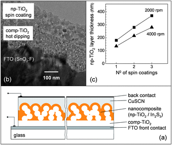 | ||
| Fig. 1 Schematic cross section of a solar cell with an ultra-thin nanocomposite absorber layer (a), transmission electron microscopy cross section of an FTO substrate coated with a “compact” comp-TiO2 layer (deposition by hot dipping) and with a nanoporous np-TiO2 (deposition by spin coating from suspension) (b) and dependence of the thickness of the np-TiO2 layer on the number of spin coatings from a nanoparticle suspension for bare glass substrates (c). | ||
Standard glass substrates coated with transparent conductive FTO, i.e.fluorine doped tin oxide (TEC8), were coated with a very dense nanocrystalline TiO2 layer (see Fig. 1(b)) in a so-called hot dipping procedure. In this simple procedure the substrate is heated to about 90 °C, dipped for a short period in a solution of 5 vol.% titanium isopropoxide (C12H28O4Ti) in 2-propanol (T20, Sigma Aldrich) and annealed in air at 450 °C for 30 min afterwards. It turned out in our experiments that such a dense nanocrystalline TiO2 layer is sufficient for insulation between the conductive FTO and the ultra-thin nanocomposite absorber layers.
Ultra-thin np-TiO2 layers were deposited by spin coating from a suspension containing TiO2nanoparticles with an average size of 20 nm (Solaronix). After each spin coating the layers were dried in air at 90 °C for 2 min. Fig. 1(b) shows the cross section of a typical substrate which has been coated with TiO2 (hot dipping) and np-TiO2 layers. The cross section was obtained with a transmission electron microscope. Spin coating was performed at various rotating speeds and tested on different substrates. The thickness of np-TiO2 layers was measured with a step profiler (Veeco Dektak8). For this purpose the np-TiO2 layers were scratched at several places before firing in air at 450 °C for 30 min. Fig. 1(c) gives examples for the dependence of the np-TiO2 layer thickness on the number of spin coatings for glass substrates at 2000 and 4000 rpm. For the given suspension and substrates the np-TiO2 layer thickness could be easily changed between 100 and 400 nm just by increasing the number of spin coatings. In the following a rotation speed of 2000 rpm was used.
In the SILAR procedure of In2S3 deposition the substrate is dipped subsequently in aqueous 0.1 M InCl3 and 0.03 M Na2S (pH = 7…8, pH was adjusted with HCl) solutions. Between the dips in the salt solutions, the samples were intensively rinsed in de-ionized distilled water. The pores of the np-TiO2 were filled completely with In2S3 after the SILAR cycling (20 cycles for the given experiments). After SILAR deposition the sample was annealed in air at 200 °C for 30 min.
The effective thickness of the In2S3 layer, i.e. the amount of In2S3 integrated over the whole nanocomposite absorber layer, was obtained by measuring the X-ray fluorescence signal of indium (In Lα) and sulfur (S Kα) with a Philips RFA MagiX pro XRF spectrometer and FP-Multi analysis software and comparing it with an In2S3 calibration standard.
Small area solar cells were completed by impregnation of the transparent CuSCN hole conductor and evaporating Au back contacts (diameter 2 mm). The solar cells were annealed at 200 °C for 4 min following previous work.5 Current–voltage characteristics were measured under illumination with a halogen lamp or under AM1.5 condition with a sun simulator. Quantum efficiency measurements were performed in the spectral range from 350 to 900 nm with chopped light and a Si reference solar cell.
Fig. 2 shows the dependence of the effective In2S3 layer thickness (deff) and of ISC and VOC on the number of spin coatings of np-TiO2 in the case of 20 SILAR cycles of In2S3 deposition. The value of deff amounted to 15 nm for the substrate uncoated with np-TiO2 and increased to 30, 52 and 72 nm after 1, 2 and 4 spin coatings, respectively.
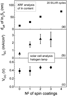 | ||
| Fig. 2 Dependence of the effective thickness of the as-deposited In2S3 layer (a) and of the short circuit current density (b) and the open circuit voltage (c) on the number of spin coatings for np-TiO2 layer deposition. The rotation speed was 2000 rpm. The number of cycles for In2S3 deposition by SILAR was 20. | ||
The values of ISC and VOC were averaged over a set of 4 preparation cycles and for each sample two selected contacts were measured. The value of ISC was 0.58 mA cm−2 for the substrate uncoated with np-TiO2 and increased to 1.79, 2.52 and 2.47 mA cm−2 for substrates with 1, 2 and 3 spin coatings of np-TiO2, respectively, for the given preparation and measurement conditions. For more spin coatings the value of ISC did not increase anymore. As a remark, solar cells were prepared on substrates with up to 10 spin coatings of np-TiO2.
I SC increased by factors of 3 (from 0 to one spin coatings) or 4.2 (from 0 to two spin coatings). At the same time, deff increased by factors of 2 and 3.2, respectively. The overall nanocomposite absorber thickness was about 200–300 nm in the case of 2 spin coatings. At this value ISC reached saturation, as opposed to deff which increased further with increasing number of spin coatings. For comparison, ISC decreased for a homogeneous In2S3 absorber layer with thicknesses increasing from 10 to 25 nm in solar cells with extremely thin absorber based on ZnO nanorod arrays.3 It can be concluded that the diffusion length of photo-generated charge carriers in the nanocomposite TiO2/In2S3 absorber is about 10 times larger in comparison to the homogeneous In2S3 absorber layer.
The value of VOC was 0.39 V for the substrate uncoated with np-TiO2, remained unchanged after one spin coating and increased to 0.47 V after 2 and 3 spin coatings (Fig. 2(c)). In contrast, VOC decreased with increasing ISC for solar cells with extremely thin absorber based on ZnO nanorod arrays.6 In general, one would expect an increase of VOC with increasing ISC. However, ISC is determined by the thickness and by the diffusion length of the nanocomposite absorber layer for solar cells with ultra-thin nanocomposite absorber or by the internal surface area for solar cells with extremely thin absorber. Recombination depends strongly on the area of the critical charge selective contact. The value of VOC may not increase or even decrease with increasing ISC if the measure leading to the increase of ISC causes a strong increase of recombination at the critical charge selective contact which is the hole extracting In2S3/CuSCN contact for the given system. Therefore, the critical contact area between In2S3 and CuSCN remained nearly constant for the solar cells with nanocomposite absorber what is not surprising if assuming a complete filling of pores in np-TiO2 with In2S3.
Fig. 3 presents the current–voltage characteristic of the best (small area) solar cell under AM1.5 illumination. This solar cell was prepared on a slightly modified substrate with a TiO2 compact layer deposited by spray pyrolysis.7 The np-TiO2 layer was deposited by 2 spin coatings and 50 SILAR cycles of In2S3 deposition were applied. The values of ISC and VOC were 8.0 mA cm−2 and 0.475 V, respectively. With the fill factor of 0.58 the energy conversion efficiency reached 2.3%. For comparison, another solar cell with 30 SILAR cycles of In2S3 deposition (deff = 55 nm) was prepared on a similar substrate and reached ISC = 7.4 mA cm−2, VOC = 0.51 V and FF = 0.44.
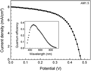 | ||
| Fig. 3 Current–voltage characteristics of the best solar cell under AM1.5 illumination. The insert shows the spectrum of the quantum efficiency. | ||
The value of ISC can be compared with ISC obtained on compact ZnO and on solar cells with extremely thin absorber based on ZnO nanorod arrays for which ISC reached 2.2 and 10 mA cm−2 with deff = 25 and 300 nm, respectively.6 Therefore, the application of ultra-thin nanocomposite absorbers allows one to reach high values of ISC with significantly less absorber material. This point may become important if taking into account limited indium resources.8
The quantum efficiency spectrum of the best solar cell gives some idea about the optimization potential. The solar cells were still opaque, they absorbed only a part of the light. Therefore the quantum efficiency was relatively low. The quantum efficiency had a maximum of 0.37 around 470 nm where the absorption coefficient is high and levelled out at wavelengths in the near infrared region around 800–850 nm. As a remark, the density of states is increased towards the near infrared due to partial diffusion of copper into In2S3.9 The partial incorporation of Cu into In2S3 leads to the decrease of the effective absorber band gap. It seems that the quantum efficiency can be further increased by applying two additional measures in the future: (i) the substrate can be additionally folded by a factor of 3–4 and, (ii) the infrared sensitivity can be increased by implementing measures of light scattering. As a remark, for structured substrates spin coating has to be replaced by another technique, for example by electrophoretic deposition of np-TiO2.10
The increase of the diffusion length of the nanocomposite absorber of photo-generated charge carriers due to local charge separation is the main advantage of ultra-thin nanocomposites. From this point of view, ultra-thin nanocomposites have to be considered for the design of inorganic high efficiency low-cost solar cells in future.
Acknowledgements
A. O. is grateful to the Deutscher Akademischer Austauschdienst (DAAD) for financial support. The authors are grateful to U. Bloeck for preparation and making the picture of the TEM (transmission electron microscopy) cross section. Furthermore, the authors are grateful to the ILGAR group of the HZB headed by C.-H. Fischer for providing the XRF calibration file.References
- M. Grätzel and B. O'Regan, Nature, 1991, 353, 737 CrossRef CAS.
- K. Taretto and U. Rau, Prog. Photovoltaics, 2004, 12, 573 CAS , and references therein.
- A. Belaidi, Th. Dittrich, D. Kieven, J. Tornow, K. Schwarzburg and M. Lux-Steiner, Phys. Status Solidi RRL, 2008, 2, 172 Search PubMed.
- Y. F. Nicolau and J. C. J. Menard, J. Cryst. Growth, 1988, 92, 128 CrossRef CAS.
- A. Belaidi, Th. Dittrich, D. Kieven, J. Tornow, K. Schwarzburg, M. Kunst, N. Allsop, M. Lux-Steiner and S. Gavrilov, Sol. Energy Mater. Sol. Cells, 2009 DOI:10.1016/j.solmat.2008.11.035.
- D. Kieven, T. Dittrich, A. Belaidi, J. Tornow, K. Schwarzburg, N. Allsop and M. Lux-Steiner, Appl. Phys. Lett., 2008, 92, 153107 CrossRef.
- A. Belaidi, S. M. Chaqour, O. Gorochov and M. Neumann-Spallart, Mater. Res. Bull., 2004, 39, 599 CrossRef CAS.
- B. A. Andersson, Prog. Photovoltaics, 2000, 8, 61 CAS.
- T. Dittrich, D. Kieven, A. Belaidi, M. Rusu, J. Tornow, K. Schwarzburg and M. Lux-Steiner, J. Appl. Phys., 2009, 105, 034509 CrossRef.
- S. Dor, Th. Dittrich, A. Ofir, L. Grinis and A. Zaban, J. Mater. Res., 2008, 23, 975 CrossRef CAS.
| This journal is © The Royal Society of Chemistry 2009 |