Computational challenges for nanostructure solar cells
Lin-Wang
Wang
Lawrence Berkeley National Laboratory, One Cyclotron Road, Berkeley, CA 94720, USA
First published on 3rd July 2009
Abstract
This review discusses the current status of large scale computational capability and future challenges for nanostructure solar cell simulations. The focus is on atomistic ab initio simulations for inorganic nanocrystal systems. A discussion of current capability in simulating the critical steps in a solar cell operation: photon absorption, exciton generation, exciton dissociation, carrier transport, and charge transfer crossing a nano contact is presented. A few novel computational methods that scale linearly to the size of the system, while retaining the ab initio quality of the simulation are introduced. Also discussed are the most challenging aspects of the simulations: surface passivation and nanocontact atomic structures.
 Lin-Wang Wang Lin-Wang Wang | Lin-Wang Wang received his BS in Physics from Shanghai Jiaotong University in 1985 and PhD in Solid State Physics from Cornell University in 1991. He worked at the National Renewable Energy Laboratory as a postdoctoral fellow and then a staff scientist from 1992 to 1999. Since 1999, he has been a staff scientist at Lawrence Berkeley National Laboratory. His main research interest is in material science simulations especially for semiconductor and nanoscale systems. He has developed various computational methods for thousand to million atom large scale electronic structure calculations. He is a recipient of the Chinese overseas outstanding young scientist award, and the 2008 ACM Gordon Bell award. He is a fellow of American Physical Society. |
Broader contextNanostructures have been proposed to be used to construct third generation solar cells. The current nanostructure solar cells often have energy efficiencies less than 3%. To be competitive with traditional solar cells, intense research effort is needed. To speed up this research, large scale computation can play an important role. Due to the recent advance in computational power and new algorithms, it is now possible to calculate the electronic structures of nanosystems with tens of thousands of atoms with ab initio accuracy. Such calculations can be used to study the photon absorption, exciton generation, exciton dissociation, carrier transport and carrier collection. The most difficult challenges are the carrier dynamics and the atomic structures of the surface and interface. In some cases, the carrier dynamics might involve both coherent and incoherent electron movements. As a result, expensive time-domain simulation might be necessary. Due to the lack of direct experimental measurements, the surface atomic structure is still by and large a mystery. Without knowing the details of such atomic structures, the surface electronic structures which can determine the carrier dynamics might not be known. Different computational strategies to deal with such problems are discussed. |
Introduction
Nanosystems have been proposed for use in photovoltaic (PV) solar cells1 and photoelectrochemical (PEC) cells.2 In PV solar cells, sunlight is converted into electricity, while in PEC cells, sunlight is used to produce a carbon-neutral chemical fuel to replace petroleum. The PEC cell works by splitting water into H2 and O2, or by converting CO2 into CO, then into other carbon hydride chemical fuels. The following discussion uses solar cell to denote both PV cells and PEC cells. The nanostructure solar cell is often called the third generation solar cell among other technologies. This follows the first generation Si thin film solar cell, and the second generation amorphous Si, CdTe, CuInSe2, Cu(In,Ga)Se2 (CIGS) thin film cells. Using nanostructure to construct solar cells has many advantages. The nanocrystals are often synthesized in relatively inexpensive ways, e.g., viavapor phase deposition in a vapor-liquid-solid (VLS) process,3 or via the solution-liquid-solid (SLS) process in a solvent.4 Although these synthesizing processes are simple, the interior of a nanocrystal can be very pure, comparable to high grade crystal ingots produced by expensive, traditional methods of crystal growth. This purity is due to the lack of dislocation in the nanocrystal and a self purification process that drives point impurities to the nanostructure surface.5 For solar cell applications, this is important because impurities often kill the photon-generated carriers, reducing the solar cell efficiency. At the same time, due to the small size of the nanosystems, the photon-generated exciton and carriers do not need to migrate far before they are collected by electrodes. This also reduces the chance of the carriers being killed. In a sense, this process resembles that used in new solar cell designs, where microelectrodes are implanted inside the active material to collect the carriers. But in nanosystems, this is done on the extreme nanoscale. Besides, other effects amplified in nanosystems can be used for various functions in a solar cell. These include: (1) quantum confinement effects that change the band gap and energy levels of the system; (2) a piezo-electric effect and permanent dipole moment, which can exert a large electric field inside the nanosystem, thus replacing the conventional p-n junction in driving the carriers into desired locations; (3) band alignment and deformation potential, which can form a staggered type-II band alignment, which again replaces the p-n junction in a thin film cell to dissociate (break down) the exciton into an electron and hole. There are also more exotic phenomena that can be used to surpass the theoretical Shockley–Queisser efficiency limit of 31% for a single junction solar cell.6 These include possible multi-exciton generation (MEG),7 and the use of the discrete quantum dot level as an intermediate band gap state to form multi-energy level solar cells.8 For nano PEC cells, the large surface to volume ratio can be beneficial. It provides an ample area for catalysis. Besides, unlike the nano PV cell, there is no need to collect the carrier out of the nanosystem, which can present a significant challenge in designing nano solar cells. To split water in a nano PEC cell, an electron and hole must be driven into different sides of a nanosystem, allowing them to generate H2 and O2, respectively. (The challenge of separating H2 from O2 can be dealt with in a separate step.) In this way, a small nanosystem can function as an independent water splitting machine, and it needs not be electrically connected to the macroscopic world. Finally, a significant advantage of using nanostructure is the ability to synthesize some alloys that cannot be synthesized as high quality thin films or bulk materials.9 This is due to the nanostructure's ability to geometrically relax elastic energy. All these provide many possibilities for revolutionary designs of nano solar cells and the development of inexpensive, highly efficient solar energy conversion.Despite the numerous advantages and potentials, there are also daunting challenges to using nanostructures in solar cell applications. At present, the dye sensitized solar cells have an energy efficiency of about 10%.10,11 In such a solar cell, the light is absorbed by the dye molecule while the TiO2nanoparticles are used only to collect the electron. However, many newly reported nano solar cells, especially those where inorganic nanostructures are used as the active light absorbing materials, have an efficiency in the range of 1–3%.12,13 This is in sharp contrast to the more mature thin film solar cell, where a Si solar cell in commercial production has an 20% efficiency,14 a CIGS thin film cell, a reported 19% efficiency,15 and a CdTe thin film cell, 16% efficiency.16 It has taken the thin film solar cell industry 50 years to improve its efficiency from the initial 6% reported by Chapin in 195417 to its current 20%. For nano solar cells to make an impact on the current energy crisis and help reduce global warming, accelerated research efforts are needed. More importantly, solar cell design and development should be based on an understanding of the critical steps in solar cell operation, not on a pure Edisonian trial-and-error experimental approach.
In a solar cell, there are a few key steps that determine overall efficiency.18 These steps are: (1) the light absorption and exciton generation; (2) the exciton dissociation into separated electron and hole; (3) the electron and hole transport, and charge transfer across nanocontacts; (4) and, in a PEC cell, the catalytic process. A few aspects of nano solar cells often limit their overall efficiency: weak absorption of light, electron–hole radiative or nonradiative recombination, nanocontact barriers, large over potentials, and slow catalytic processes in a PEC cell. Unfortunately, in a nano solar cell, many of these processes and steps are not well understood. In some steps, like the light absorption and exciton dissociation, the quantitative aspects are not well known. In other steps, like the carrier transport, charge transfer, nonradiative recombination, and catalysis, even the qualitative picture is missing. All these hinder our ability to design more efficient solar cells. Designing a cell structure with confidence about its performance is important, because, experimentally, it might take years to realize one particular solar cell design. Theoretical simulation can play an important role in this design process. Simulation can also help in testing new materials. In many ways, the new material is as important, if not more important, than the nanosystem design. For example, for a water-splitting PEC cell, it is critical to have the active material's highest occupied molecular orbital (HOMO) and lowest unoccupied molecular orbital (LUMO) levels sandwich the water oxidization (to produce O2) and reduction (to produce H2) levels. Meanwhile, the material must be corrosion-resistant because it will be submerged in water. Such materials are difficult to find. Usually oxides are corrosion resistant. But unfortunately, oxides always have a very low HOMO level, much lower than the water oxidization level.19 This low HOMO level results in waste because of the excessive over potential in the oxidation side. One approach is to make alloys using anions with less electron negativity. For example, if O is mixed with N, the HOMO level might be raised, as evident in the GaN:ZnO alloy.20 Simulation can help one to understand and design such new materials.21
Simulating the aforementioned critical steps requires extensive computing power. In terms of large scale computation, we are in an exciting era. We have just witnessed the world's fastest computer passed the petaflops milestone.22 The high performance computing (HPC) community is geared up for exascale computing, characterized by a billion Gflops. That is similar to having a billion personal computers at one's disposal, provided efficient parallel programs and algorithms exist to take advantage of such computers. With a petaflop computer, even if the nanosystem has one million atoms, there will be roughly one computer processor for each atom, provided a linear scaling algorithm can be used. With all this computing power, new ways can be devised to carry out simulations and tap into new phenomena that were previously too difficult to simulate. The next part of this review, will discuss the current status and future perspective of simulating the critical steps in nanostructure solar cells. This will be mostly drawn from personal research and personal perspectives. No attempt is made at a comprehensive review of this vast topic. The focus will be on inorganic nanocrystals, and will discuss the physics issues and computational challenges. The vast topics of catalytic processes and new material designs will not be discussed here since there are already many excellent reviews on these topics.23,24 Instead, the focus will be on nanostructure related properties and simulations.
The basic formalism
There are many computational approaches that can be used to study the optical and electronic properties of nanosystems. For a solar cell with either a traditional thin film or a nanostructure, the first fruitful and simple simulation can be the semiclassical Poisson-drift diffusion equation.25 This can provide an overall picture of the device, especially if the system is relatively large, for example, in the 100 nm range. This approach uses the semiclassical formula to calculate the local charge density at a given point, r, based on the quasi local Fermi energy and the band edge (conduction band and valence band) positions. It then uses the Poisson equation to calculate the Coulomb potential and yields a self-consistent charge–potential relationship. The zero order approximation of the Boltzmann equation, the drift diffusion equation, is used to describe the current as proportional to the gradients of charge density and the potential. In Fig. 1, the band bending of a cylindrical nanowire is shown. In this hypothetical nanowire with a 100 nm radius, for the first 50 nm core, the system is doped as n-type with a doping level of 2 × 1017 cm−3. However, outside the 50 nm shell, the system is not doped. The solution of the semiclassical simulation shows that there could be a band bending of 70 meV from the perimeter of the nanowire to its center. This bending could be large enough to drive the electron carrier to the center and the hole carrier to the perimeter, thus it functions as a traditional p-n junction. This p-n junction without p-type doping is important because, in many materials, due to the dopant pinning rule,26 there can only be one type of doping (e.g., no p-type for oxides). In a nanosystem, due to the different geometry than the bulk, the result of the Poisson equation is also different. Thus, it is not sufficient to use the bulk results (e.g., p-n junction depletion layer thickness) to estimate the nanostructure results. Actual simulation using the Poisson-drift diffusion equation is often necessary and can be very useful.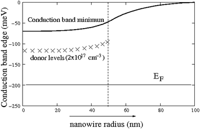 | ||
| Fig. 1 The band bending in a nanowire where the core of the wire (for r < 50 nm) is n-type doped, while the rest of the wire is undoped. The doping level is 2 × 1017 cm−3, while the system is calculated at room temperature. | ||
The above Poisson-drift diffusion equation is a good model for micron-sized systems. However, for nano solar cells, the dimension of the system may be smaller than the mean free path of the carrier in the Boltzmann equation. Thus the use of the drift equation is questionable. Besides, the local density of states at position r probably cannot be described by the corresponding semiconductor bulk formula. This is especially true near the interfaces where the potential change can be rapid and quantum confinement effects can be large.27 Thus, although this semiclassical simulation can be useful for providing an overall picture, especially for nano cells larger than 100 nm, the quantitative results might not be reliable for smaller cells. For very small cells, even the qualitative picture could be wrong.
To improve on the semiclassical simulations quantum mechanical effects need to be introduced. One way to do so is to use the effective mass, or k.p. model Hamiltonian for the electrons.28 The corresponding equations are simple to solve, and they were developed from bulk semiconductors for impurity and quantum well studies.29 However, when the system size reduces to a few nanometers, the effective mass method also suffers from inaccuracy.30 Besides, there are problems with these envelope-based models, for example, in matching the envelope functions crossing a heterostructure interface and in treating the atomic details of the system. This review focuses on atomistic ab initio calculations.
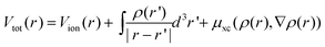
The discussion is restricted to density functional theory (DFT) calculations.31–33 In recent years, DFT has become the method of choice for the majority of material science simulations. This is in part due to the maturity of the method and the knowledge of what it can and cannot do. It is also partially due to the dissemination of some popular and easy to use computer programs such as the Vienna Ab initio Simulation Package (VASP) code34 and the Gaussian code.35 There are a few popular approximations of the DFT method. One is local density approximation (LDA),36 another is generalized gradient approximation (GGA),37 and a third is the hybrid method (e.g., the B3LYP).38 The essence of these methods is to solve N single electron wave function ψi, i = 1,N, here 2N is the number of electrons. This is a major simplification of the original many-body equation. The single particle Kohn–Sham equation32 can be written as:
 | (1) |
 , and the total charge density
 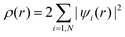 . Here, µxc(ρ(r),∇ρ(r)) is the exchange–correlation potential at r, which depends only on the local charge density ρ(r) (in LDA36) or its gradients ∇ρ(r) (in GGA37 and B3LYP38). The third term in eqn (1) is a nonlocal pseudopotential term, in the Klaiman–Bylander projector form.39 This term only exists in the pseudopotential approach, for example, when plane waves are used as the wave function expansion basis set.40 The last exchange integral term in eqn (1) only appears in a hybrid method like B3LYP.38Eqn (1) is a nonlinear equation, which is often solved self-consistently using iterative methods.40
With the modern super computer and thousands of processors, the above equation can be used to solve problems with a thousand atoms41 (for LDA or GGA). Ten thousand atom systems can also be calculated using the real space grid method.42 However, such calculations can take weeks, thus it is not very feasible for routine studies. The large computer time stems from its O(N3) scaling of the computational cost. This is mainly to enforce the orthonormal constraint among the wave functions: 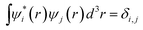 . The following discussion introduces some alternative methods, which scale as O(N), and can be used to study thousand- or ten-thousand–atom systems with ease, while retaining the same ab initio accuracy as in the direct DFT calculations.
The DFT was originally designed to calculate the total energy, and the use of its Kohn–Sham equation eigen energies to represent the electronic structure is questionable.43 However, later it was realized that there are direct connections between the Kohn–Sham eigen energy and the electron energy level in a real system.44,45 Thus, conceptually, there is a basis to use the eigen energies of the Kohn–Sham equation to interpret electronic structure. In practice, many people are doing just that. Nevertheless, the most reliable treatment for the electronic structure is based on the many-body perturbation theory, the GW (the name is derived from its formula) equation,46 which describes the quasiparticle wave functions. The GW equation is similar to the Kohn–Sham equation, but replaces the exchange correlation terms µxc(ρ,∇ρ) and 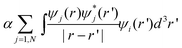 with the self energy term
 . Unfortunately, the direct calculation of the GW equation for a nanosystm is often impractical. As a result, a discussion of ways to approximate the GW equation in nanostructure calculations is presented.
Electronic structures and optical properties of heterostructure nanosystems
For systems a few nanometers in size, doping is difficult to achieve. Even if it can be done experimentally, the average number of doping atoms in a nanosystem is probably only a few. This will result in large fluctuations in dopant numbers, which can make the device not repeatable. Thus, in many nano solar cell designs, heterostructure is used to replace the effects of doping. A type II bind alignment (with one material's conduction band and valence band both higher than another material's counterparts) can be used to fill the role of a p-n junction in a traditional solar cell. To simulate such a device, the first step is to calculate the basic electronic structures and optical properties of such hetero nanosystems. These include the single electron states and their wave function localizations and eigen energies.For an atomistic calculation, before any simulation can be carried out, the atomic structure needs to be determined. The first challenge is to decide the surface passivation. As will be discussed later, this is one of the most difficult problems. For many systems, the exact surface passivations and their atomic structures is simply not known. At this stage, most calculations have been performed by assuming an idealistic surface passivation. For example, for a Si quantum dot, an H passivation with atomic relaxation can be used following the atomic structures on flat surfaces.47,48 For other systems, for example, CdSe and InP, artificial pseudo-hydrogen atoms with partial charges of 1.5, 0.5, 1.25, 0.75 electrons have been used.49,50 These passivations are analogous to the Si–H passivation and thus represent the ideal theoretical passivations. But obviously, in reality, no such pseudo-hydrogen atom exists. One of the future improvements will be to introduce realistic surface passivation models and study their effects. Although there are cases where the surface passivation will affect the properties of the interior electronic structures, in many cases, as long as the surface states are moved away from the band gap, the details of the passivation will have a minimum effect on the interior electronic structures. These are the cases presented here.
As most heterostructures are lattice mismatched, the next step is to relax the elastic energy to get the atomic positions. Fortunately, this can be done using a valence force field (VFF) model.51VFF is a ball and stick model to describe the elastic energy based on bond stretching and bond angle bending mechanical energies. This model has been shown to be very accurate for elastic energy calculations. It is better than the continuous model because it can capture the atomic features (e.g., the symmetry and local atomic relaxation) of the nanostructures. The VFF relaxed atomic positions can be very close to the DFT relaxed results for systems like GaInAs. This approach has been used by many groups.52,53 However, more tests may be necessary to establish the reliability of the VFF model, especially for describing surface relaxations. Currently, surface atoms (e.g., the pseudo-hydrogen atoms discussed above) have been allowed to relax freely, without constraints. In reality, the surface atom might reconstruct, which tends to exert a compressive strain.54 As a result, a single material quantum dot (e.g., CdSe) might have its lattice expand a little in regions close to the center, but be compressed a little at the surface layer. These phenomena are closely related to the surface passivation model, as will be discussed later.
After the atomic positions are determined, one can solve the self-consistent Kohn–Sham equation to yield the charge density and total potential V(r). If the system has about one thousand atoms or less, this can indeed be done by either using the VASP code,34 which uses a plane wave basis, or the PARSEC code,55 which uses a real space grid. However, for systems with even larger number of atoms, these direct approaches quickly become unfeasible. Fortunately, there are other methods in such situations. The first one is a charge patching method (CPM).56,57 The CPM generates the atomic charge density motifs from small prototype system calculations, then patches them together to construct a nanosystem. This is based on the assumption that the charge density at a given point r only depends on the bonding environment around r. The CPM yields very good charge densities compared to the direct DFT method (within 1%). The subsequent error in the eigen energy is about 20 meV when compared with direct DFT calculations.57 The patched charge density can then be used to generate the potential V(r) by solving the Poisson equation and using LDA or GGA formula for the exchange correlation potential µxc(ρ(r),∇ρ(r)). After that, for the cases of LDA or GGA methods, the Hamiltonian H of the Kohn–Sham equation is known. The subsequent question is to solve the Kohn–Sham eigen states: Hψi = εiψi. If traditional methods are used, as in the direct DFT calculations, where all the N occupied wave functions must be calculated, this will lead to an O(N3) algorithm again. Fortunately, for most electronic structures and optical properties, only the eigen states near the band edge are needed. Thus, a folded spectrum method (FSM)58 is used to solve these band edge states without calculating all the N lower energy states. This FSM solves (H − Eref)2ψi = (εi − Eref)2ψi instead of the original Hψi = εiψi, where Eref is a constant, placed inside the band gap. Using the preconditioned conjugate gradient method to solve the end of spectrum state, the first wave function solved in FSM is the band edge state. As a result, the computational cost scales as O(N). Using the generalized moments method,59 the density of state of a given nanosystem for the whole energy range can also be calculated in an O(N) scaling.
The “pseudo-H passivation, VFF atomic relaxation, CPM and FSM” approach has been used to study many heterostructure nanosystems. One example is shown in Fig. 2, where a CdTe nanowire is calculated.60 The high excited state optical absorption spectrum is calculated based on the single particle energy level, εi, and the electron–hole Coulomb interaction energy. As can be seen, the peaks of the optical absorption spectrum agree perfectly with the experimental measurements, demonstrating the accuracy of this approach.
![Experimentally measured optical absorption spectrum (upper panels) for CdTe nanowires with different diameters ((a) 5.3 nm; (b) 7.3 nm; (c) 10.2 nm), compared with the calculated optical absorption spectrum (lower panels). In the upper panels, the dashed lines represent background absorption and the colored peaks are the decomposed transition peaks from the measured absorption spectrum. [Taken from Ref. 56 with permission from ACS].](/image/article/2009/EE/b904805g/b904805g-f2.gif) | ||
| Fig. 2 Experimentally measured optical absorption spectrum (upper panels) for CdTe nanowires with different diameters ((a) 5.3 nm; (b) 7.3 nm; (c) 10.2 nm), compared with the calculated optical absorption spectrum (lower panels). In the upper panels, the dashed lines represent background absorption and the colored peaks are the decomposed transition peaks from the measured absorption spectrum. [Taken from Ref. 56 with permission from ACS]. | ||
In Fig. 3, CdSe embedded in a CdS nanorod is calculated following the above approach. Such nanostructures have been synthesized experimentally,61 but their electronic structure, especially their wave function localizations, cannot be measured directly. Theoretical calculations can shed light on this important issue. As shown in Fig. 3, in the calculated result, the electron is outside the CdSe core, while the hole stays inside the core. There are several factors which determine the localization of the electron and hole wave functions. The first is the band alignment between CdSe and CdS. The system has a type I natural band alignment (where the deformation potential due to the lattice mismatch is not taken into account), which means both electron and hole should stay inside the CdSe core. However, the deformation potential, which accounts for the band energy change due to elastic strain, changes this picture. As the CdSe core is compressed, its electron conduction band energy increases in absolute value. As a result, the electron moves outside the core. Another possible effect is the piezoelectric potential. In wurtzite crystal structure, along the c-axis, there is no inversion symmetry. Any stress can cause a piezoelectric field in that direction. In this particular case, however, the piezoelectric field is found to be small, not a main factor for the state localization.
 | ||
| Fig. 3 A CdSe core (inside the red dashed line) embedded in a CdS nanorod. The blue isosurface is the hole wave function, while the green isosurface is the electron isosurface. The atomic positions are relaxed with VFF, while the charge density is obtained with the charge patching method, and the electron eigen states are solved using the folded spectrum method. | ||
In the above examples, the electronic wave functions and eigen energies are calculated using DFT Hamiltonian. There is a well known band gap problem for LDA and GGA approximation of DFT.62 In practice, this band gap error is significantly reduced in B3LYP, although this might be just a fortuitous effect of the hybridization of the LDA and Hartree–Fock, not result of fundamental causes.63 In the above examples, this problem was solved by modifying the LDA Hamiltonian to fit the crystal bulk band structure. This was done by changing the s, p, d nonlocal pseudopotentials in eqn (1) to move the position of the conduction band while keeping the position of the valence band unchanged. The resulting LDA + C (correction) Hamiltonian was used for nanostructure calculations.64 This relies on the assumption that the valence band alignment of LDA is good. However, this might not always be the case.
There are two sources of errors when one uses the LDA (or GGA) Kohn–Sham equation to represent the GW quasi-particle equation. [This is equivalent to using the LDA exchange correlation potential µxc(ρ(r)) to represent the GW self energy term Σ(r,r′,εi).] First, the self-energy term Σ(r,r′,εi) has a long range effect. This is due to the system dielectric function ε(r,r′,ω) which is used in the GW self-energy expression. This dielectric function has a long range image charge polarization effect in a heterostructure. This image polarization potential can be approximated as:65
 | (2) |
![Surface polarization potential P(r) for a CdSe tetrapod. represent the individual atoms. The potential is shown on a cross section through two of the four tetrapod legs. On the cross section, the pink color is positive while the blue color is negative. [Taken from Ref. 61, with permission from ACS].](/image/article/2009/EE/b904805g/b904805g-f4.gif) | ||
Fig. 4 Surface polarization potential P(r) for a CdSe tetrapod.  represent the individual atoms. The potential is shown on a cross section through two of the four tetrapod legs. On the cross section, the pink color is positive while the blue color is negative. [Taken from Ref. 61, with permission from ACS]. represent the individual atoms. The potential is shown on a cross section through two of the four tetrapod legs. On the cross section, the pink color is positive while the blue color is negative. [Taken from Ref. 61, with permission from ACS]. | ||
The second error is directly related to the bulk band gap error of LDA.43 This is caused by the error in µxc(ρ(r)) when compared to Σ(r,r′,εi) for a pure bulk system.66 The fact that Σ(r,r′,εi) is nonlocal (but short ranged in a pure bulk system) has some significance. If a pure local potential is added to µxc(ρ(r)) to correct the band gap error, it is often found that the resulting effective mass will be too large. This is because a pure local potential does not add any oscillator strength  between the valence band and the conduction band. But increasing LDA EP is necessary to yield the correct effective mass. One possible future improvement is to compare the GW bulk eigen energies with the LDA bulk eigen energies.66 This can not only correct the band gap, it can also correct each individual band energy (i.e., separately correct the valence band and conduction band). One can also try to write a separable form to approximate bulk Σ(r,r′,εi), and use that approximated self-energy in nanostructure calculations.
The approach discussed here can be used to simulate nanostructures specifically designed for nano size solar cells. Fig. 5 shows one such design using a ZnO/ZnS core/shell nanowire.67,68 Oxides are abundant and chemically stable. But one of their problems is their large band gaps. One idea to achieve a smaller band gap (hence increase the PV efficiency) is to have a small type-II core/shell structure as with ZnO/ZnS. In this case, a photon absorption can pump one electron from the valence band of ZnS to the conduction band of ZnO. This effectively reduces the band gap of the whole system from the original 3.4 eV to 2.1 eV, thus significantly increasing the theoretical solar cell efficiency. The calculation shows that if the system is small, this absorption can be strong enough for solar cell applications. Another advantage of such core/shell nanowire type-II band alignment is that the electron and hole can be separated immediately after they are generated. Furthermore, the calculation indicates that the HOMO and LUMO levels do not have any oscillator strength due to symmetry. As a result, the electron can travel in the ZnO shell while the hole travels in the ZnS core without the danger of optical recombination, which is a major carrier loss mechanism in many oxides.
![A small ZnO/ZnS core/shell nanowire (a). The electron will stay in the ZnO core, while the hole will stay in the ZnS shell. The original bulk ZnO band gap (around 3.4 eV) and ZnS band gap (around 3.7 eV) have been reduced to 2.07 eV, as shown in the calculated optical absorption spectrum (b). This can increase the Shockley–Quiesser theoretical efficiency of the solar cell to 23%. [Taken from Ref. 63, with permission from ACS].](/image/article/2009/EE/b904805g/b904805g-f5.gif) | ||
| Fig. 5 A small ZnO/ZnS core/shell nanowire (a). The electron will stay in the ZnO core, while the hole will stay in the ZnS shell. The original bulk ZnO band gap (around 3.4 eV) and ZnS band gap (around 3.7 eV) have been reduced to 2.07 eV, as shown in the calculated optical absorption spectrum (b). This can increase the Shockley–Quiesser theoretical efficiency of the solar cell to 23%. [Taken from Ref. 63, with permission from ACS]. | ||
For all the above examples, CPM was used to generate the LDA charge density, hence its potential Vtot. However, there are cases where the CPM method cannot be used. One example is the total dipole moment of a quantum dot.69 The permanent dipole moment has important effects on the behavior of a nanosystem. For example, it can help the quantum dots to self assemble into perfect super-crystal structures.70 Internally, such a dipole moment can induce an internal electric field, which can significantly change the state localization inside the system. This permanent electric field can also be used in solar cell design to separate the electron and hole. For a small nanosystem, such an electric field can be stronger than the one induced by doping. To study this permanent dipole moment, it is, however, necessary to solve the charge density self-consistently. One can of course use the original direct LDA or GGA method. But much more efficient linear scaling methods can be used to carry out such total energy self-consistent calculations. Here, a linear scaling three dimensional fragment (LS3DF) method is introduced.71,72 The LS3DF divides the system into many small fragments, and calculates the wave functions and charge densities of each fragment separately, using a group of computer processors. As the system grows larger, there are more fragments (while the fragment size is fixed), thus more processor groups can be used to solve them. This provides a perfect parallelization to the number of processors, meanwhile the total computational cost is proportional to the number of fragments, thus the total number of atoms. Fig. 6 shows the parallelization scaling of the LS3DF code on different machines. For the largest run, it scaled up to 150,000 processors on a Cray XT5 machine at Oakridge National Laboratory. In total, it reached 442 Tflops. After the fragment charge densities are obtained, they are patched together to get the charge density of the whole system with a novel scheme. This patching scheme assures that the artificial fragment surface effects, due to the system subdivision, will be cancelled out among the fragments. The patched charge density will then be used to solve a global Poisson equation for the global potential. An outside loop will be iterated, which will yield self-consistency between the input and output global potentials. Due to the use of the novel patching scheme, the LS3DF is very accurate, with its results (including the dipole moments) essentially the same as the original direct DFT calculations;71,72 but it can be a thousand times faster for systems with >10,000 atoms.
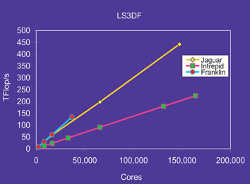 | ||
| Fig. 6 The parallelization scaling for the LS3DF code on three different machines: Jaguar, Cray XT5 machine at the National Center for Computational Science (NCCS) at Oakridge National Laboratory; Intrepid, IBM BlueGene/P machine at Argonne Leadership Computing Facility (ALCF) at Argonne National Laboratory; and Franklin, Cray XT4 machine at National Energy Research Scientific Computing Center (NERSC) at Lawrence Berkeley National Laboratory. This is a weak scaling result, which means when the number of cores (computer processors) increases, the physical size of the problem also increases accordingly. | ||
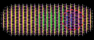
Fig. 7 shows two differently shaped quantum dots (one as a pancake, another as a rod). The total dipole moment of a dot consists of a surface contribution and a bulk contribution. The LS3DF calculation shows that the bulk contribution not only depends on the volume of the quantum dot, but also on the shape of the dot. As a result, for the two dots in Fig. 7, although they have the same volume, their bulk dipole moment contributions are different. This is because there is a self-screening effect, and the efficiency of this screening depends on the shape of the quantum dot.
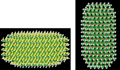 | ||
| Fig. 7 Two different shaped CdSe quantum dots. While their total number of atoms are similar, the bulk contributions to the total dipole moments are very different. The pancake shaped quantum dot (left) has a bulk contribution to the dipole moment at 30.3 Debye, while for the cigar shaped quantum dot (right), this contribution is 73.3 Debye. The dipole moments are calculated using the LS3DF method. | ||
Exciton calculations
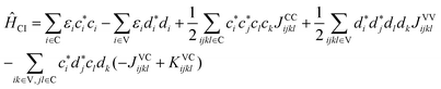
Exciton energies and wave functions need to be calculated to obtain the optical absorption spectrum and to study the exciton dissociation. In the so-called strong quantum confinement regime where the quantum dot size is smaller than the bulk exciton radius, the correlation effect is very small. In these cases, the exciton wave function is a simple product of electron and hole single particle wave functions. However for the exciton energy, besides the single particle eigen energies, it is necessary to include the screened Coulomb interaction and exchange interaction between the electron and hole. More generally, a four body Coulomb interaction integral can be defined as:73 | (3) |
 | (4) |
![The Auger processes, which have been calculated using the limited CI approach. The calculated Auger life time is typically in sub picoseconds, which agrees well with the experimental observations. [Taken from Ref. 72, with permission from APS].](/image/article/2009/EE/b904805g/b904805g-f8.gif) | ||
| Fig. 8 The Auger processes, which have been calculated using the limited CI approach. The calculated Auger life time is typically in sub picoseconds, which agrees well with the experimental observations. [Taken from Ref. 72, with permission from APS]. | ||
Another approach to study excitons is to calculate the exciton wave functions explicitly in a variational form. This is a very intuitive way to study exciton binding energy and dissociation. As mentioned above, in many cases, the correlation effect is small, and the exciton wave function can be approximated as a simple product of the electron and hole wave functions. One can take the wave functions from the neutral system Hamiltonian, and calculate the Coulomb interactions from eqn (3). However, this does not take into account the fact that the Coulomb interaction can cause wave function localizations. Imagine a nanowire with the left side consisting of material A and the right side consisting of material B. If the A/B connection has a type II band alignment, the electron will stay in A and the hole will stay in B. But at the interface, they can still form an exciton with an electron/hole Coulomb attraction localizing their wave functions close to the interface. This localization is important in studying the exciton dissociation. In order to get this wave function localization, the Coulomb potential needs to be included in the single particle Schrodinger's equation. Thus:
 | (5) |
 is the screened Coulomb potential due to the hole wave function ψV. There is a similar equation for the hole wave function ψV. These two equations need to be solved self-consistently between ψC and ψV.
For relatively small systems where direct LDA calculation is possible, eqn (5) is similar to a constraint LDA calculation, where a valence band state is kept unoccupied while a conduction band state is occupied. The self-consistency of all the occupied electrons plays the role of screening. Fig. 9 shows one such calculation for a β-carotene molecule attached to a C60 buckyball.79 One can see that the electron is localized at the buckyball while the hole is localized at the β-carotene molecule. In this case, the electron–hole separation is large, and the Coulomb interaction between them is relatively small.
![The electron (pink) on C60 and hole (blue) on β-carotene in an exciton calculated with constraints DFT method. The C60–β-carotene attachment atomic structure is studied based on DFT total energy. [Taken from Ref. 75, with permission from AIP].](/image/article/2009/EE/b904805g/b904805g-f9.gif) | ||
| Fig. 9 The electron (pink) on C60 and hole (blue) on β-carotene in an exciton calculated with constraints DFT method. The C60–β-carotene attachment atomic structure is studied based on DFT total energy. [Taken from Ref. 75, with permission from AIP]. | ||
If one of the nanostructure dimensions is infinite, as in a nanowire, the correlation effect does play an important role in localizing the electron and hole wave functions.80 In such a case, a single product of the electron and hole wave function can no longer be used to represent the exciton wave function. One possibility is to add a Jastrow function, thus  ; here the Jastrow function can be
  , where z is in the wire axis direction. Using this exciton wave function, the energy of the exciton can be efficiently calculated with the help of the Fast Fourier Transformation (FFT) to evaluate the Jastrow function related integrals. Unfortunately, strictly speaking, this exciton wave function is not correct. According to eqn (4), in an exciton wave function Ψexciton(re,rh), the Hilbert space spanned by re must fall into the subspace spanned by all the conduction bands:
 . Similarly, the Hilbert space spanned by rh must fall into the subspace spanned by all the valence bands:
 . Unfortunately, the above Jastrow function containing Ψexciton(re,rh) does not satisfy this constraint. As a result, the wave function needs to be projected back to its proper subspace. This can be done by making approximations in its energy evaluation.81
Carrier transport and charge transfer
One of the most challenging tasks in simulating a nano solar cell is to calculate the carrier transport. As discussed before, the mean free path of a bulk free carrier is usually longer than the dimension of the nanosystem. Thus, the semiclassical drift diffusion equation probably cannot be used. It is very likely that even the Boltzmann equation cannot be used either, because the eigen state energies are discrete. A more fundamental question is whether one can use the Fermi golden rule to describe the transition from one state to another (e.g., by absorbing phonons). In some systems, due to the thermal fluctuation and the change of the atomic positions, the electron eigen energies change very quickly, in the order of sub picoseconds.82 This eigen energy change can be faster than the average time of transition. Thus, the use of the Fermi golden rule, which assumes constant state energies during the transition period, becomes questionable. In some other cases, when there is a strong surface (or interfacial, or defect) phonon/electron coupling, multiple phonon effects might be important. This also makes the transport and charge transfer calculations based on simple models difficult.83 Nevertheless, one approach is to calculate the electron–phonon coupling constants: , for all the phonon modes ν. Using the CPM, the ∂H/∂ν can be calculated quickly without doing self-consistent calculations for each phonon mode. The phonon modes can be calculated based on the VFF model. After all the coupling constants are calculated, the phonon-assisted incoherent hopping transport can be calculated, including the cases of multiple phonon transitions for deep state trapping and nonradiative decays.
In the most difficult carrier transport and charge transfer problems, the coherent and incoherent electron movements might both be important, and the conformational change of the nanostructure (or molecular atomic structure) might induce large coherent adiabatic state changes between the incoherent hopping movements. These problems can be simulated directly using time-domain methods.84–87 In these time-domain methods, the electron wave functions are progressed following the time dependent Schrodinger's equation, while the movement of nuclei are evaluated using molecular dynamics (MD). In some sense this is like the real time evaluation of the time-dependent DFT (TDDFT) method.88 But here, the movement of nuclei is also included, and instead of carrying out the simulation for femtoseconds like in most real time TDDFT calculations, the time-domain simulations need to be carried out for picoseconds or longer, until the electron transition happens. Another significant difference from the TDDFT is that there is a process for state collapsing (hopping) to the adiabatic states in the time-domain method.89 This is a process that represents the quantum de-phasing (incoherent movement), corresponds to, for example, the phonon assisted hopping. The long time duration makes the time-domain simulation extremely expensive. Currently only tight-binding models or very small systems are calculated. Because of the computational expense, it is usually necessary to make some approximations. One approximation is to decouple the time dependent Schrodinger's equation with the nuclei MD. This is a good approximation provided the electron state is not very localized and strongly coupled with one or two phonon modes. Thus, the movements of the atoms are not strongly influenced by the existence of the carriers. By making this approximation, one can use a classical model like the VFF to carry out the nuclei MD.
The time dependent Schrodinger's equation  is usually carried out by decomposing the wave function ψ into the adiabatic eigen states
  . Here ψi(t) is the eigen state of H(R(t)): H(R(t))ψi(t) = εi(t)ψi(t). If
  , then:
 | (6) |
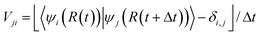 . So, in this approach, one large computational cost comes from repeatedly solving the eigen states
  . In an empirical tight-binding Hamiltonian, H is only determined by atomic positions R(t). However, in an ab initio approach, H is determined by the occupied states
  . Note, in a sudden switch method for state collapsing, as described by Tully,89 these occupied states (which are not necessarily the N lowest eigen energies but N adiabatic eigen states) remain occupied before another jump happens. This is despite the fact that the wave functions ψ(t) are no longer the adiabatic eigen states during this time period. In other words, the occupied states are
  , not ψ(t).
One can also use the CPM to accelerate the time-domain calculation. In the CPM, H(R(t)) can be constructed from the atomic positions, without the calculation of all the occupied states. ψ(t) can still be evaluated using eqn (6). However, if only the transitions among a few states near the band edge are of interest, then eqn (6) can be expanded only among the few states in the j index summation. In this way, only a small number of states near the band edge need to be calculated using FSM. Including only the states with similar energies in eqn (6) will also help to increase the time step dt to evaluate eqn (6).
Fig. 10 shows the results of charge transfer crossing an Alizarin molecule (a chromophore) and a small TiO2 dot simulated by using the time-domain method.82 The excited electron is initially in Alizarin conduction band states, then quickly (within 100 fs) moves to a TiO2cluster, then moves back to Alizarin (within 660 fs) to occupy the empty valence state (the molecular ground state). This shows how an exciton can be dissipated by nonradiative decay. Such a process is often the major reason for low quantum efficiency in many nano sized solar cells.
![A TiO2/Alizarin nanocontact (a), with carrier dynamics simulated using the time-domain method (b). In (a), the large gray spheres are Ti, red spheres are O, smaller white spheres are H, and black spheres are C. In (b), an exciton is first generated in the chromophore Alizarin molecule at time zero. Initially, the electron occupies the LUMO, LUMO + 1 and LUMO + 2 states, and stays at the Alizarin side. Within about 100 fs, the electron moves to TiO2. However, in the following 660 fs, the electron moves back to Alizarin to refill the valence band state. This is indicated by the increase of the population of the Alizarin ground state (indicated by in (b)). [Taken from Ref. 78, with permission from ACS].](/image/article/2009/EE/b904805g/b904805g-f10.gif) | ||
Fig. 10 A TiO2/Alizarin nanocontact (a), with carrier dynamics simulated using the time-domain method (b). In (a), the large gray spheres are Ti, red spheres are O, smaller white spheres are H, and black spheres are C. In (b), an exciton is first generated in the chromophore Alizarin molecule at time zero. Initially, the electron occupies the LUMO, LUMO + 1 and LUMO + 2 states, and stays at the Alizarin side. Within about 100 fs, the electron moves to TiO2. However, in the following 660 fs, the electron moves back to Alizarin to refill the valence band state. This is indicated by the increase of the population of the Alizarin ground state (indicated by ![[thick line, graph caption]](https://www.rsc.org/images/entities/char_e117.gif) in (b)). [Taken from Ref. 78, with permission from ACS]. in (b)). [Taken from Ref. 78, with permission from ACS]. | ||
The time-domain method is one of the most expensive computational methods. How to accelerate the calculation and effectively use modern computers with hundreds of thousands of processors remains a challenge.
Atomic structures of surface passivation and nanocontact
Surface passivation and atomic structure are among the biggest challenges in nanostructure simulations. Currently, the atomic structure of a nanocrystal surface is largely unknown. This is partly due to the lack of experimental tools to probe the surface atomic structure of nanosystems, and partly because it is extremely difficult to determine the surface structure by brute force direct simulations. In terms of accuracy, the DFT, perhaps with some additional way to include the van der Waals interactions (e.g., using the truncated van der Waals potential90), should be accurate enough to describe the atomic interactions and the resulting atomic structures. The challenge here is with the large number of possible atomic configurations, and the long simulation time needed to truthfully describe the real dynamics via an MD simulation.The surface atomic structure is important in many aspects. The surface trapping state is one of the most important potential sources for carrier loss in a nano solar cell. The surface atomic structure can also affect the carrier dynamics and carrier cooling. For example, experiments have shown that the multi-exciton generation might depend sensitively on surface ligand types.91 Given the large surface to volume ratio in nanosystems, it is not difficult to appreciate the extreme importance of surface structure and its influence on the electronic structures and carrier dynamics of the whole system.
The surface situation for nanosystems also varies tremendously from case to case. For example, for a hexagonal shaped ZnO nanowire,92 the non polar surface is dimerized, and no organic ligand is needed for its passivation. The surface passivation of a Si quantum dot by H and O atoms is well studied and relatively well understood.47,48 The surface passivation for a CdSe quantum dot is, however, more complicated. There is a report of self-healing reconstruction, where a quantum dot without surface ligand passivation can still have a highly efficient photoluminescence.93 However, usually, the surfaces of CdSe, CdS, and CdTe quantum dots are passivated with trioctylphosphine oxide (TOPO) or other organic ligands.94 Only a limited number of theoretical studies have been reported on the surface passivation of these quantum dots.95–97 One small system ab initio MD simulation confirms the existence of the self-healing effect (removing the dangling bond states) by self-reconstruction.98 Flat surface ligand passivations are calculated to shed light on quantum dot surface passivation. Recently, calculations have also been carried out directly on small quantum dot surfaces, especially using the magic numbered Cd33Se33 quantum dot.54
Another class of problems is the attachment between a molecule (e.g., a dye molecule) or a polymer and a nanostructure. This is the case for the dye sensitized solar cell. Numerous theoretical works have connected molecules to C60 and carbon nanotubes. Due to their limited possible attachment configurations, such problems are well suited for theoretical investigations. These attachments constitute one form of nanocontacts. But many nanocontacts are between a metal electrode (e.g., a spherical Pt nano dot) and a semiconductor nanocrystal (e.g., a CdS nanowire). The atomic structures, and the possible defect states of such nanocontacts are still poorly understood. Unlike semiconductor to semiconductor interfaces, where coherent epitaxial interfacial connections are often formed, many of the semiconductor/metal interfaces are noncoherent. Understanding the atomic structures and electronic states in the interface is extremely important.
There are several different theoretical approaches to studying the surface passivation and nanocontacts. The most common approach is to select a few feasible passivation structures, then use direct LDA or GGA calculations to relax the atomic positions to their local minima, and then compare the total energies of these different passivation structures. The initial guess might come from simpler flat surface calculations or experimental measurements, or from chemical bonding intuitions. Currently, this is the most widely used method, especially when a molecule is attached to a semiconductor surface. Fig. 9 shows one such example.79
The second approach is a direct ab initio MD simulation. In many cases, these can be applied locally, focusing on the most important area (e.g., the connecting area in a semiconductor/metal nano contact). Due to its extreme time consuming nature, this approach has been used only rarely. But given the increasing computer power and the maturity of many computer codes like VASP34 and CPMD,99 more and more usage of such direct simulations are expected.
In another approach, one can start with an ideal but artificial passivation (e.g., using the pseudo-H atoms), then remove a few of these pseudo-H atoms, replacing them with ligand molecules, or letting the atoms reconstruct locally. In this way, one can isolate a single defect state on the surface, and study its coupling and effects on the interior electronic structures.
Overall, the surface passivation and possible surface trapping states are the least understood aspects of nanostructure simulations. In order to accurately predict the efficiency of a nano solar cell, it is of paramount important to study these surface effects. Future large-scale simulations might play an important role in this regard.
Conclusions
A brief discussion of the computational approaches and challenges for nanostructure solar cells has been presented. Such nano solar cells include PV and PEC cells. For such nano structure solar cells to have a significant impact on the energy market and to do so quickly enough to help reduce global warming, theoretical simulation is critical for understanding the fundamental physics and accelerating the nano solar cell research. This discussion was focused on inorganic nanocrystals and the key steps in the operation of a nano solar cell. These steps include photon absorption, generation of the exciton, exciton dissociation, carrier transport, and charge transfer across the nano contact. The catalytic process for water splitting in a nano PEC cell was not discussed because it is a huge topic in itself. The emphasis here was on simulations of the nanostructure device as a whole, and on atomistic ab initio calculations. Also emphasized was the current status of computational approaches and capability, instead of the physical results of the simulations. With modern super computers and the developments of new algorithms, it is now possible to calculate the optical absorption and the exciton generation with relatively high fidelities. There are still challenges, especially in correcting the DFT band energy errors. One suggestion is to compare the bulk DFT results with bulk GW results. Exciton dissociation can also be studied by calculating the exciton wave functions and binding energies. One can use the CI approach or variational wave function approach for the exciton calculations. The carrier transport and charge transfer across a nanocontact is more challenging. There are cases where such transports can be studied by combining traditional transport models with static ab initio calculations (e.g., electron localizations and electron–phonon coupling, or electron–electron coupling and scattering). There are also cases where simple models may not be applicable. In those cases, direct time-domain simulations might be necessary. These time-domain simulations are extremely expensive. Currently, only empirical Hamiltonians or very small systems are used in such simulations. However, with the growth of computer power and improved algorithms, more of these simulations are expected. The simulations can also be used to study surface and defect-state carrier trapping, and electron–hole nonradiative recombination—very important issues that often determine the quantum efficiencies of solar cells. Finally, the biggest challenge is the uncertainty of the surfaces and their passivations. Without a realistic model for the surface passivation, one does not have a complete picture of the whole device. Thus, the final efficiency of the solar cell cannot be predicted with certainty. There is no single simulation approach to study the surface, instead, different approaches need to be used. Direct ab initio MD simulation might be too expensive and need to run too long to reveal the real passivation pattern. One common approach is to compare the energies of intuitively guessed passivation patterns. Perhaps long molecular dynamics simulation based on special ab initio fitted classical force field models can play an important role. New experimental methods capable of probing the surface atomic structure will certainly be most helpful. Overall, given the continued growth of computer power (not in processor speed, but in the total number of processors) and the development of new algorithms that can effectively take advantage of these increasing powers, large-scale simulations are expected to play a critical role in nanostructure solar cell research.Acknowledgements
This work was supported by the DMSE/BES/SC of the US Department of Energy under the contract No. DE-AC02-05CH11231. Some of the calculations shown in this paper used the resources of the National Energy Research Scientific Computing Center (NERSC), Oakridge Leadership Computing Facility (OLCF), and Argonne Leadership Computing Facility (ALCF). This work is also supported by the US Department of Energy Innovative and Novel Computational Impact on Theory and Experiment (INCITE) program.References
- P. V. Kamat, J. Phys. Chem. C, 2007, 111, 2834 CrossRef CAS
.
- D. A. Tryk, A. Fujishima and K. Honda, Electrochim. Acta, 2000, 45, 2363 CrossRef CAS
- Y. Wu and P. Yang, J. Am. Chem. Soc., 2001, 123, 3165 CrossRef CAS
- T. J. Trentler and
et. al.
, Science, 1995, 270, 5243
- S. C. Erwin and
et. al.
, Nature, 2005, 436, 91 CrossRef CAS
- W. Shockley and H. J. Queisser, J. Appl. Phys., 1961, 32, 510 CAS
- R. D. Schaller and V. I. Klimov, Phys. Rev. Lett., 2004, 92, 186601 CrossRef CAS
- A. Luque and A. Marti, Phys. Rev. Lett., 1997, 78, 5014 CrossRef CAS
- T. Kuykendall, P. Ulrich, S. Aloni and P. Yang, Nat. Mater., 2007, 6, 951 CrossRef CAS
- R. O'Regan and M. Gratzel, Nature, 1991, 353, 737 CrossRef CAS
-
Y. Chiba, A. Islam, K. Kakutani, R. Komiya, N. Koide, L. Han, Technical Digest, 15th International Photovoltaic Science and Engineering Conference, Shanghai, October 2005, 665–666 Search PubMed
- W. U. Huynh, J. J. Dittmer and A. P. Alivisatos, Science, 2002, 295, 5564
- B. Tian and
et. al
, Nature, 2007, 449, 885 CrossRef CAS
- M. A. Green, K. Emery, Y. Hishikawa and W. Warta, Solar Cell Efficiency Tables (Version 32), Prog. Photovoltaics, 2008, 16, 435 CAS
- K. Ramanathan and
et. al.
, Prog. Photovoltaics, 2003, 11, 225
- T. Aramoto and
et. al.
, Jpn. J. Appl. Phys., Part 1, 1997, 36, 6304 CrossRef
- D. M. Chapin, C. S. Fuller and G. L. Pearson, J. Appl. Phys., 1954, 25, 676 CAS
-
M. A. Green, Third Generation Photovoltaics: Advanced Solar Energy Conversion, Springer Verlag, Heidelberg, 2003 Search PubMed
- C. G. Van De Walle and J. Neugebauer, Nature, 2003, 423, 626 CrossRef CAS
- K. Maeda and K. Domen, J. Phys. Chem. C, 2007, 111, 7851 CrossRef CAS
- L. L. Jensen, J. T. Muckerman and M. D. Newton, J. Phys. Chem. C, 2008, 112, 3439 CrossRef CAS
- http://www.top500.org/lists/2008/11 .
- A. Chatterjee, Int. J. Mol. Sci., 2002, 3, 234 Search PubMed
- A. Franceschetti and A. Zunger, Nature, 1999, 402, 60 CrossRef CAS
-
S. M. Sze, Semiconductor Devices, John Wiley & Sons, Inc. 2001 Search PubMed
- W. Walukiewicz, Physica B, 2001, 302–303, 123 CrossRef
- J. W. Luo, S. S. Li, J. B. Xia and L. W. Wang, Appl. Phys. Lett., 2007, 90, 143108 CrossRef
- G. A. Baraff and D. Gershoni, Phys. Rev. B, 1991, 43, 4011 CrossRef
-
E. O. Kane, in Semiconductor and Semimetals, ed. R. K. Willardson and A. C. Beer, Academic Press, New York, 1966, Vol. I, p. 75, Search PubMed
- H. Fu, L. W. Wang and A. Zunger, Appl. Phys. Lett., 1997, 71, 3433 CrossRef CAS
- P. Hohenberg and W. Kohn, Phys. Rev., 1964, 136, B864 CrossRef
- W. Kohn and L. J. Sham, Phys. Rev., 1965, 140, A1133 CrossRef
-
W. Koch and M. C. Holthausen, A Chemist's Guide to Density Functional Theory, Wiley-VCH, Weinheim, 2000 Search PubMed
- http://cms.mpi.univie.ac.at/vasp/ .
- http://www.gaussian.com/g_ur/g03mantop.htm .
- J. P. Perdew and A. Zunger, Phys. Rev. B, 1981, 23, 5048 CrossRef CAS
-
J. P. Perdew, S. Kurth, in A Primer in Density Functional Theory, ed. C. Fiolhais, F. Nogueira and M. A. L. Marques, Springer, Berlin, 2003 Search PubMed
- A. D. Becke, Phys. Rev. A, 1988, 38, 3098 CrossRef CAS
- L. Kleinman and D. M. Bylander, Phys. Rev. Lett., 1982, 48, 1425 CrossRef CAS
- M. C. Payne, M. P. Teter, D. C. Allan, T. A. Arias and J. D. Joannopoulos, Rev. Mod. Phys., 1992, 64, 1045 CrossRef CAS
- D. R. Hummer, J. D. Kubicki, P. R. C. Kent, J. E. Post and P. J. Heaney, J. Phys. Chem. C, 2009, 113, 4240 CrossRef CAS
- J. Chelikowsky, APS Bull., 2005, 51, 612 Search PubMed
- R. W. Goodby, M. Schulter and L. J. Sham, Phys. Rev. B, 1988, 37, 10159 CrossRef
- A. Gorling, Phys. Rev. A, 1992, 46, 3753 CrossRef
- C. Filippi, C. J. Umrigar and X. Gonze, J. Chem. Phys., 1997, 107, 9994 CrossRef CAS
- L. Hedin, Phys. Rev., 1965, 139, A796 CrossRef
- J. P. Wilcoxon and
et. al.
, Phys. Rev. B, 1999, 60, 2704 CrossRef CAS
- M. V. Wolkin and
et. al.
, Phys. Rev. Lett., 1999, 82, 197 CrossRef CAS
- L. W. Wang and A. Zunger, Phys. Rev. B., 1996, 53, 9579 CrossRef CAS
- H. Fu and A. Zunger, Phys. Rev. B, 1998, 57, R15064 CrossRef CAS
- C. Pryor, J. Kim, L. W. Wang, A. Williamson and A. Zunger, J. Appl. Phys., 1998, 83, 2548 CrossRef CAS
- R. H. Miwa, P. Venezuela and A. Fazzio, Phys. Rev. B, 2003, 67, 205317 CrossRef
- A. Marbeuf, M. Barbe, A. Ramos, C. Levelut and S. Wszolek, Acta Crystallogr., 1994, 50, 326
- H. Kamisaka, S. V. Kilina, K. Yamashita and O. V. Prezhdo, J. Phys. Chem. C, 2008, 112, 7800 CrossRef CAS
- http://parsec.ices.utexas.edu/publications/index.html .
- L. W. Wang, Phys. Rev. Lett., 2002, 88, 256402 CrossRef
- L. W. Wang and J. Li, Phys. Rev. B, 2004, 69, 153302 CrossRef
- L. W. Wang and A. Zunger, J. Chem. Phys., 1994, 100, 2394 CrossRef CAS
- L. W. Wang, Phys. Rev. B, 1994, 49, 10154 CrossRef CAS
- J. Sun, W. E. Buhro, L. W. Wang and J. Schrier, Nano Lett., 2008, 8, 2913 CrossRef CAS
- L. Carbone and
et. al.
, Nano Lett., 2007, 7, 2942 CrossRef CAS
- C. Geller and
et. al.
, Appl. Phys. Lett., 2001, 79, 368 CrossRef CAS
- A. J. Cohen, P. Mori-Sanchez and W. Yang, Science, 2008, 321, 792 CrossRef CAS
- J. Li and L. W. Wang, Phys. Rev. B, 2005, 72, 125325 CrossRef
- L. W. Wang, J. Phys. Chem. B, 2005, 109, 23330 CrossRef CAS
- B. Lee, L. W. Wang, C. D. Sparatus and S. G. Louie, Phys. Rev. B, 2007, 76, 245114 CrossRef
- J. Schrier, D. O. Demchenko, L. W. Wang and A. P. Alivisatos, Nano Lett., 2007, 7, 2377 CrossRef CAS
- Z. Yang, L. W. Wang and A. Mascarenhas, Nano Lett., 2007, 7, 1264 CrossRef CAS
- M. Shim and
et. al.
, J. Chem. Phys., 1999, 111, 6955 CrossRef CAS
- D. V. Talapin and
et. al.
, Adv. Mater., 2001, 13, 1868 CrossRef
- L. W. Wang, Z. Zhao and J. Meza, Phys. Rev. B, 2008, 77, 165113 CrossRef
- Z. Zhao, J. Meza and L. W. Wang, J. Phys.: Condens. Matter, 2008, 20, 294203 CrossRef
- A. Franceschetti, L. W. Wang, H. Fu and A. Zunger, Phys. Rev. B, 1998, 58, R13367 CrossRef CAS
- A. Franceschetti, H. Fu, L. W. Wang and A. Zunger, Phys. Rev. B, 1999, 60, 1819 CrossRef CAS
- G. Strinati, Phys. Rev. B, 1984, 29, 5718 CrossRef CAS
- L. W. Wang, M. Califano, A. Zunger and A. Franceschetti, Phys. Rev. Lett., 2003, 91, 56404 CrossRef
- Al. L. Efros, V. A. Kharchenko and M. Rosen, Solid State Commun., 1995, 93, 281 CrossRef CAS
- J. M. An, A. Franceschetti and A. Zunger, J. Chem. Phys., 2008, 128, 164720 CrossRef
- T. Baruah and M. R. Pederson, J. Chem. Phys., 2006, 125, 164706 CrossRef
- J.-B. Xia and K. W. Cheah, Phys. Rev. B, 1997, 55, 1596 CrossRef CAS
- J. Schrier, L. W. Wang (unpublished).
- W. R. Duncan, C. F. Craig and O. V. Prezhdo, J. Am. Chem. Soc., 2007, 129, 8528 CrossRef CAS
- J.-L. Breda, D. Beljonne, V. Coropceanu and J. Cornil, Chem. Rev., 2004, 104, 4971 CrossRef CAS
- W. M. Stier and O. V. Prezhdo, J. Phys. Chem. B, 2002, 106, 8047 CrossRef CAS
- W. R. Duncan, W. M. Stier and O. V. Prezhdo, J. Am. Chem. Soc., 2005, 127, 7941 CrossRef CAS
- S. G. Abuabara, L. G. C. Rego and V. S. Batista, J. Am. Chem. Soc., 2005, 127, 18234 CrossRef CAS
- S. Ramakrishna, F. Willig, V. May and A. Knorr, J. Phys. Chem. B, 2003, 107, 607 CrossRef CAS
- K. Burke, J. Werschnik and E. K. U. Gross, J. Chem. Phys., 2005, 123, 62206 CrossRef
- J. C. Tully, J. Chem. Phys., 1990, 93, 1061 CrossRef CAS
- H. Sun, J. Phys. Chem. B, 1998, 102, 7338 CrossRef CAS
- M. Ben-Lulu, D. Mocatta, M. Bonn, U. Banin and S. Ruhman, Nano Lett., 2008, 8, 1207 CrossRef
- S. Xu and
et. al.
, J. Am. Chem. Soc., 2008, 130, 14958 CrossRef CAS
- Z. A. Peng and X. Peng, J. Am. Chem. Soc., 2002, 124, 3343 CrossRef CAS
- A. P. Alivisatos, Science, 1996, 271, 5251
- A. Puzder, A. J. Williamson, F. Gygi and G. Galli, Phys. Rev. Lett., 2004, 92, 217401 CrossRef
- L. Manna, L. W. Wang, R. Cingolani and A. P. Alivisatos, J. Phys. Chem. B, 2005, 109, 6183 CrossRef CAS
- J. Y. Rempel, B. L. Trout, M. G. Bawendi and K. F. Jensen, J. Phys. Chem. B, 2006, 110, 18007 CrossRef CAS
- A. Puzder, A. Williamson, N. Zaitseva, G. Galli, L. Manna and A. Alivisatos, Nano Lett., 2004, 4, 2361 CrossRef CAS
- http://www.cpmd.org/ .
| This journal is © The Royal Society of Chemistry 2009 |