Integrated blocking layers for hybrid organic solar cells
Mine
Memesa
a,
Stefan
Weber
a,
Sebastian
Lenz
a,
Jan
Perlich
c,
Rüdiger
Berger
a,
Peter
Müller-Buschbaum
c and
Jochen S.
Gutmann
*ab
aMax-Planck Institute for Polymer Research, Ackermannweg 10, 55128, Mainz, Germany. E-mail: gutmann@mpip-mainz.mpg.de; Fax: +49 6131 379 100; Tel: +49 6131 379 117
bInstitute of Physical Chemistry, University Mainz, 55099, Mainz, Germany
cTechnische Universität München, Physik Department E13, James-Frank-Str. 1, 85747, Garching, Germany
First published on 30th March 2009
Abstract
In hybrid organic solar cells a blocking layer between transparent electrode and nanocrystalline titania particles is essential to prevent short-circuiting and current loss through recombination at the electrode interface. Here we report the preparation of a thin, uniform and crack free hybrid blocking layer composed of conducting titania nanoparticles embedded in an insulating polymer derived ceramic. To do so we combine sol–gel chemistry with novel poly(dimethylsiloxane) containing amphiphilic block copolymer, poly(ethyleneglycol) methyl ether methacrylate–block–poly(dimethylsiloxane)–block–poly(ethyleneglycol) methyl ether methacrylate as the templating agent. Conductive probe scanning force microscopy proved that the existing percolating titania networks are separated by an insulating ceramic matrix. The structural uniformity of the percolating structures was investigated by microbeam grazing incidence small angle X-ray scattering making the integrated blocking layer suitable for hybrid organic solar device applications. Preliminary tests with the integrated blocking layer showed reasonable comparison to conventional TiO2 blocking layer containing devices mentioned in the literature.
Broader contextOrganic solar cells have been the focus of active research for almost 20 years. They promise reduced costs because their synthesis takes place at lower temperatures and they can be manufactured from liquid solutions using well established printing techniques. Their performance however is significantly lower than the performance of silicon based solar cells and thus every single functional layer in such a device has to be optimized. A central active part in many organic solar cells is a so called ‘blocking layer’ which reduces unwanted short circuits at the electrode interface. Commonly this layer is monolithic and rather thick. We demonstrate an alternative approach to prepare thinner blocking layers; where smarter chemistry incorporates the insulator into nm gaps between the conductive pathways in a manner that does not increase the complexity of device preparation. To prove the concept we also image the spacing of conductive and non-conductive surface domains on a nm scale, analyzing the heterogeneity of charge percolation through electronically active organic layers with an unprecedented level of detail. |
Introduction
Dye-sensitized titanium dioxide (TiO2) solar cells developed by Grätzel et al.1 where a liquid electrolyte is used for charge transport, are among the most efficient organic solar cells.2 However the presence of a liquid electrolyte as the charge transport medium creates sealing problems. As alternatives conjugated p-type polymers, hole transport compounds with triarylamine structural units, low molecular weight spiro-compounds or inorganic p-type semiconductors are tested as charge transport media to prepare solid state solar cells.3–8 Sealing problems are thus solved by switching to solid state electrolytes. However the short-circuit and current loss through charge recombination at the interface between the transparent fluorine doped tin oxide (FTO) electrode and the hole transport medium resulted in intrinsically inefficient solar cells. Grätzel and co-workers put an additional compact layer of TiO2 between the FTO and nanocrystalline TiO2 layer and increased the current output by three to four orders of magnitude. Even when the transparent FTO electrode is replaced with graphite, the use of a blocking layer is inevitable because of the ohmic contact formed between graphite and hole conducting material.9 TiO2 blocking layers are conventionally prepared by electron beam evaporation,10chemical vapor deposition from Ti3O5 under oxygen partial pressure11 or tetraisopropylorthotitanate,12 aerosol pyrolysis deposition,13spray pyrolysis of titanium(IV)bis(acetoacetonato)di(isopropanoxylate)14 or by sol–gel methods using titanium isopropoxide.15Preparation of mesoporous metal–alkoxides with controlled morphology using amphiphilic block copolymers as templating agents in combination with sol–gel chemistry is well established.16,17 This strategy has been extended to the preparation of titania nanoparticles18–20 opening pathways to potential application in dye-sensitized hybrid organic solar devices. Recently, we showed that poly(dimethylsiloxane) (PDMS) could be used as a spin-on barrier layer for titania particles.21 To allow conduction through titania particles the surface of the embedded titania particles has to be exposed, which is easily achieved by a short plasma treatment. However, during plasma treatment cracks occurred within the insulating PDMS film due to crosslinking. To overcome crack formation in the PDMS coating and to yield an integrated insulation layer, we propose to incorporate PDMS via one block of the templating amphiphilic block copolymer. The templated titania particles are exposed at the surface after a short plasma etch which removes the top PDMS layer. Annealing under inert gas is required to convert the PDMS into a polymer derived silicon oxycarbide (SiOC) type ceramic and transfer the titania into the anatase polymorph. This step is performed under nitrogen to exclude oxygen which would result in burning of the PDMS before ceramization. Integration of the PDMS into the amphiphilic block copolymer therefore localizes the insulating polymer derived ceramic between the semiconducting titania particles. An effective blocking layer has to be thick enough to prevent any cracks and shorts and thin enough to keep the series resistance at a minimum. In conventional approaches, a compact TiO2 blocking layer of around 100 nm thickness is needed to achieve a homogenous, well packed layer over the transparent electrode.14 Recently Kuwabata et al.22 investigated and found the optimum thickness of the TiO2 blocking layer prepared by spray pyrolysis to be between 30–40 nm for quantum dot sensitized solar cells. The purpose of our study is to replace the conventional blocking layer with a thinner, more easily processable and morphologically controlled hybrid blocking layer with a clear potential for a reduction in the serial resistance.
Results and discussion
(PEO)MA–PDMS–MA(PEO) synthesis
Poly(ethyleneglycol) methyl ether methacrylate–block–poly(dimethylsiloxane)–block–poly(ethyleneglycol) methyl ether methacrylate [(PEO)MA–PDMS–MA(PEO)] triblock copolymer was synthesized by atom transfer radical polymerization (ATRP) of poly(ethyleneglycol) methyl ether methacrylate after preparation of a difunctional PDMS macroinitiator. Synthesis steps are shown in Scheme 1. 1H-NMR spectral peaks showing successful macroinitiator preparation and block copolymer synthesis are given in the experimental section. The broad peak at 2.05 ppm corresponding to the hydroxyl groups on dihydroxyl end-functionalized PDMS (1) disappeared and two singlet peaks appeared at 1.94 ppm, 2.00 ppm ((CH3)2CBr) after esterification reaction with 2-bromo-2-methylpropionyl. This difunctional macroinitiator, (2), was used for ATRP of poly(ethyleneglycol) methyl ether methacrylate [(PEO)MA] monomer. Double bond hydrogen peaks, 6.04 ppm and 5.49 ppm, of the monomer disappeared after polymerization, and the triblock copolymer peaks were: PEO methylene triplet at 3.64 ppm, singlet at 3.37 ppm for methyl ether at the end of the PEO chain and singlet for PDMS methyl groups at 0.05 ppm. The number-average molecular weight of the triblock copolymer is about Mn = 9300 g mol−1 with polydispersity D = 1.68 (Fig. 1).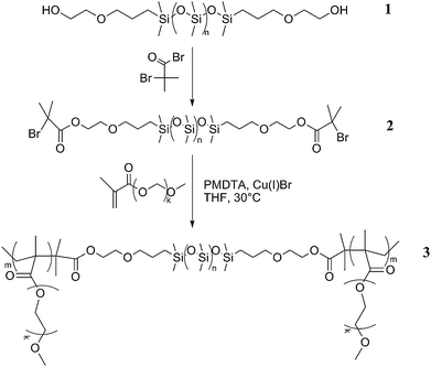 | ||
| Scheme 1 (PEO)MA–PDMS–MA(PEO) (3) amphiphilic block copolymer synthesis steps. | ||
 | ||
| Fig. 1 Molecular weight distribution of (PEO)MA–PDMS–MA(PEO) (3). | ||
(PEO)MA–PDMS–MA(PEO)/titania nanocomposite films
(PEO)MA–PDMS–MA(PEO)/titania nanocomposite films were prepared as explained in the experimental section. After the nanocomposite films were prepared, plasma and heat treatments were applied as depicted in Scheme 2. The titania surface was exposed by plasma cleaning to enable electrical conduction through the film. To embed the exposed anatase particles into a polymer derived insulating ceramic matrix, the films were subsequently heated to 450 °C under an inert gas atmosphere to avoid pyrolysis of the PDMS block before ceramization. The electronic properties of “SiOC” type ceramics are strongly influenced by the presence or absence of carbon precipitates.23 To exclude carbon precipitation during ceramization, a pure (PEO)MA–PDMS–MA(PEO) triblock copolymer sample was annealed at 450 °C under nitrogen. The white appearance of the polymeric residue after annealing (Fig. 2) shows no evidence of carbon precipitation and the polymer derived SiOC ceramic can therefore be expected to act as an insulator. | ||
| Scheme 2 The plasma and heat treatment scheme applied to nanocomposite films. | ||
 | ||
| Fig. 2 A polymer derived ceramic: The white colour shows that no carbon precipitates are formed at 450 °C. | ||
In Fig. 3, the X-ray diffraction pattern of (PEO)MA–PDMS–MA(PEO)/titania nanocomposite film shows typical anatase TiO2 peaks after annealing at 450 °C under nitrogen. The standard anatase TiO2 diffraction lines24 are drawn below the observed peaks. ‘As prepared’ nanocomposite films show no peaks corresponding to an amorphous titania phase after sol–gel synthesis. As seen from the X-ray diffraction pattern annealing at 450 °C converts the titania into anatase. Although annealing under an oxygen atmosphere is desirable with respect to oxygen defects,25 to convert PDMS into a ceramic material the heating must be performed under an oxygen free atmosphere to prevent burning of PDMS before ceramization. The (PEO)MA–PDMS–MA(PEO)/titania nanocomposite films are composed of anatase titania and polymer derived ceramic after plasma treatment and annealing at 450 °C.
 | ||
| Fig. 3 XRD diffractogram of the titania/(PEO)MA–PDMS–MA(PEO) nanocomposite film (A) after annealing at 450 °C under nitrogen, and (B) ‘as prepared’. The standard anatase TiO2 diffraction lines24 are drawn below the observed peaks. | ||
The existence of an electrically conductive network of titania particles surrounded by an insulating layer is proven by scanning conductive probe microscopy (CPM).26,27 Samples containing 2% titania precursor were prepared on a 50 nm thick sputtered Pt electrode on Si wafers. A constant bias voltage of 3800 mV between the Pt electrode and the CPM tip was applied during contact mode imaging in order to obtain a current map of plasma treated and annealed samples (Fig. 4a). The topography (Fig. 4a1) shows a granular structure with a typical grain diameter of 10–15 nm and density of approximately 1000 per µm2 as counted from a 1 × 1 µm2 image. These grains are attributed to titania particles at the surface. The resulting current map (Fig. 4a2) reveals about 600 spots on an area of 1 µm2 carrying currents of up to 5 pA. Thus we conclude that roughly 60% of the titania particles at the surface are electrically interconnected to the Pt electrode. Furthermore, dark areas of some 100 nm in width were mapped where no conduction was observed. To correlate high and low currents directly with the topography, areas carrying currents <1 pA (i.e. dark blue) were made transparent. The resulting image was then combined with the topography image (Fig. 4a3). In this plot highly conductive areas were found with similar probability on elevations and in depressions. Large poorly conducting areas can be associated with elevations (e.g. the center of the image, 2–6 nm in height) existing on the surface at a density of 1–2/µm2. These elevations are caused by polymer derived SiOC, resulting in insulation. Furthermore, the tiny holes observed in the film have a diameter of 10 nm and a depth of up to 5 nm, shown as white circles in Fig. 4a1 and a2. These holes are associated with the highest currents measured during CFM. At these spots modifications may have occurred during imaging with CFM if a certain local current density was exceeded. This explanation is further supported by analysis of the same sample in non-contact mode, which reproduced all topographical features, except for the measurement induced holes.
 | ||
| Fig. 4 CPM image of (PEO)MA–PDMS–MA(PEO)/titania nanocomposite film plasma treated/annealed at 450 °C, and control sample of only (PEO)MA–PDMS–MA(PEO) film annealed at 450 °C. Topography (a1), current map (a2) and combined (a3) images of plasma treated/annealed nanocomposite film and polymer film after annealing at 450 °C as a reference sample (b1,2). | ||
To prove that the conductive sites imaged in Fig. 4a originate from the titania integrated into the hybrid film, a control measurement of a pure (PEO)MA–PDMS–MA(PEO) polymer film ceramized at 450 °C under nitrogen was performed (Fig. 4b). In the ceramized polymer film holes with a diameter of 100–200 nm and depth of 10 nm were observed. The corresponding conductivity map shows no current flow through the polymer at a bias voltage of 1000 mV. However the holes carry a current in the order of nA, which is two orders of magnitude larger than the peak current in our integrated barrier layer. Such a current is typical for pinholes in polymer films, i.e. it acts as a short circuit between CFM tip and the Pt electrode. This control measurement also reveals the necessity of plasma treatment in order to expose the conductive surface of the titania nanoparticles. If the titania surface is not exposed prior to ceramization, the resulting insulation layer will prevent any electrical contact with the thick nanocrytalline TiO2 layer in potential dye-sensitized TiO2 solar cell devices.
CPM has a resolution on the femtoampere scale. Measured currents are six orders of magnitude larger (corresponding to the short circuits in the control sample) and three orders of magnitude larger (through the titania network) in the integrated blocking layer than the resolution limit of the technique. From these CPM experiments we concluded that we had successfully prepared an integrated blocking layer consisting of a conductive network of titania particles embedded in an insulating polymer matrix.
Application of the integrated blocking layer in actual devices requires film homogeneity over large surface areas. In previous studies we observed crack formation in PDMS homopolymer films with plasma treatment.21 A large area SEM showed no crack formation of the templated hybrid films with plasma treatment, and after subsequent annealing at 450 °C (Fig. 5a and b), due to crosslinking of the PDMS film via the titania nanoparticles. In contrast a plasma treated PDMS homopolymer control without internal crosslinking showed sizeable (µm) cracks21 (Fig. 5c).
 | ||
| Fig. 5 SEM images of titania/(PEO)MA–PDMS–MA(PEO) nanocomposite film (a) after plasma treatment and (b) after plasma and heat treatment at 450 °C under nitrogen are compared to (c) plasma etched PDMS film.21 | ||
The effect of each preparation step on titania morphology was further investigated on samples prepared from stock solutions containing 1% titania precursor by raising the heating temperature beyond 450 °C to 600 °C and 1000 °C. As a reference a pristine nanocomposite sample (film thickness 42 ± 3 nm) was imaged without any treatment prior to the measurement (Fig. 6a). Without plasma treatment the free film surface is smooth. However 10 min of plasma treatment resulted in a characteristic surface morphology consisting of circular pits (Fig. 6b, film thickness 28 ± 2 nm) which are the result of a liquid/liquid phase separation during spin coating.28 Further heating reduces surface roughness; however the pits remain present at the surface (Fig. 6c–e). The thickness of the integrated blocking layer (plasma treated/annealed at 450 °C) is calculated as 18 ± 1 nm from X-ray reflectivity measurement (Fig. 7), which was modeled using the Parratt program.29 Within the surface depressions, i.e. circular pits, smaller titania particles are again present, as observed by scanning force microscopy (SFM) and scanning electron microscopy (SEM) (Fig. 8). This proves that an insulating matrix is formed throughout the whole film.
 | ||
| Fig. 6 SFM height images of titania/(PEO)MA–PDMS–MA(PEO) nanocomposite films (a) ‘as prepared’, (b) plasma treated, (c) plasma treated/annealed at 450 °C, (d) plasma treated/annealed at 600 °C, and (e) plasma treated/annealed at 1000 °C. | ||
 | ||
| Fig. 7 X-ray reflectivity of the integrated blocking layer (plasma treated/annealed at 450 °C). The film thickness was fitted using Parratt formalism (Parratt32, HMI). | ||
 | ||
| Fig. 8 Higher magnification analysis of plasma treated/annealed at 1000 °C sample, (a) SFM height image and (b) SEM image from one of the dark circular regions in Fig.6e. | ||
Microscopy techniques are restricted to investigation in the micrometer range. To prove the uniformity of the titania morphology over larger lateral length scales, and to investigate the lateral structure of the titania particles µGISAXS measurements were performed. µGISAXS scattering patterns yield averaged structural information of the illuminated sample spots. In our case this sample spot was of size 1781 × 32 µm2. This is a consequence of the enlarged footprint at the chosen incident angle of 0.74° and is 225![[thin space (1/6-em)]](https://www.rsc.org/images/entities/char_2009.gif) 000 times larger than the surface area imaged in Fig. 4. Out of plane cuts, at an exit angle equal to the critical angle of titania, αc = 0.28°, were performed (Fig. 9) enabling us to obtain averaged structure information about the percolating titania structures in the range several nanometers to ∼200 nm.
000 times larger than the surface area imaged in Fig. 4. Out of plane cuts, at an exit angle equal to the critical angle of titania, αc = 0.28°, were performed (Fig. 9) enabling us to obtain averaged structure information about the percolating titania structures in the range several nanometers to ∼200 nm.
 | ||
| Fig. 9 GISAXS curves with fits overlaid for ‘as prepared’ (○) and plasma treated/annealed at 450 °C (△) samples, the dashed line represents the resolution limit. The table gives the values from the Unified Fit Model for packing (P) and radius of gyration (Rg). | ||
For a closer data analysis, the out of plane cuts presented in Fig. 9 were fitted according to the Unified Fit Model.30–32 This model consists of a combination of Guinier and Porod regimes over multiple structural levels. It was successfully applied to various scattering experiments in transmission geometry for different applications.31–37 Since incident and exit angles are fixed, the Unified Fit Model can also be applied to diffuse surface scattering from film samples using grazing incidence geometry. This model describes the structure of the material in structural levels, from single particles to clusters. Each level contains: a Guinier regime which describes the size, and a power-law regime which gives the integral properties of the structure. Starting from the high q-regime, experimental data shows Porod regime indicated by the constant slope in the log-log plot from q > 0.05 Å−1. This power-law regime is followed by a shoulder like Guinier regime until q ≈ 0.012 Å−1. Scattering of this first structural level is followed by another Porod and Guinier regime. The low-q resolution limit resulting from the size of the primary beam at the CCD detector was q < 0.0056 Å−1. Therefore, scattering from the second Guinier regime is limited by the resolution limit. However, the resolution limit was small enough to derive meaningful values for the radius of gyration, Rg, of the second level. The curve progression did not substantially change for the pristine and plasma treated/annealed at 450 °C sample indicating the stability of the structure; of the titania particles in the polymer matrix upon plasma and heat treatment. The table in Fig. 9 shows the obtained values of the Unified Fit Model for both samples. The smallest structures obtained from the fits, corresponding to the high-q region, are the same within experimental error with a Rg of ∼80 Å and an average particle–particle distance of ∼250 Å which did not change after plasma etching and heat treatment. The power-law exponent, P, gives information about the packing and character of the particles. For compact spherical particles, P is expected to be 4. The power-law exponent of ∼1.9 obtained from the fit is far from the power-law exponent of compact spherical particles. This can be explained by primary titania particles, which consist of a solid titania core covered by a rough titania shell with integrated PEO chains. Ulrich et al.17 reported that the metal–alkoxide particles prepared by sol–gel chemistry show rough surfaces with incorporated PEO blocks. The PEO chains decompose during heating, leaving porous titania behind. SFM imaging of nanocomposite films annealed to 1000 °C (Fig. 8a) show polydisperse particles of diameter 200 Å without uniform shape which is in agreement with the X-ray analysis. The second level from the Unified Fit Model has a size of Rg = (1695 ± 17) Å in the pristine sample and Rg = (2139 ± 13) Å for the plasma treated/annealed at 450 °C sample. These values match the sizes of the circular regions observed (Fig. 5a and c) for the ‘as prepared’ and plasma treated/annealed samples. µGISAXS data analysis by the Unified Fit Model confirmed that the features observed by microscopy techniques accurately represent the structure of the integrated barrier layer over large surface areas.
Application potential in hybrid organic solar cells
Preliminary tests on hybrid organic solar cells to prove the concept of an alternative blocking layer were done using the integrated blocking layer. In these tests an additional nanocrystalline titania layer was not used because the exposed titania surface itself should be able to generate a photocurrent. Although these films do not lead to a very efficient solar cell device they allow a check to determine if the barrier layer concept works in principle. The current–voltage (I–V) characteristics of the device showed a short-circuit photocurrent density (Isc) of 0.03 ± 0.003 mA cm−2 with an open-circuit voltage (Voc) of 0.42 ± 0.04 V, calculated fill factor (FF) of 0.30 ± 0.01, and overall power conversion efficiency of 0.0035 ± 0.0005%. A comparable type of device consisting of only a conventional TiO2 blocking layer was tested by McGehee et al.38 where (Isc) of 0.83 mA cm−2 with an open-circuit voltage (Voc) of 0.64 V and fill factor (FF) of 0.58 and overall efficiency of 0.31% was observed. In order to compare the values stated by McGehee with our devices, it is necessary to compensate for differences in surface area between the two devices. In the study by McGehee the conventional barrier layer consisted of 100% titania where the complete surface is available for dye absorption. Our hybrid blocking layer has a total thickness of ∼18–19 nm of which only the exposed titania surface (3–4 nm in height Fig. 4a1) is accessible for dye absorption. Assuming that only the dye-sensitized surface contributes to the photocurrent our integrated barrier layer would exhibit only 17–20% of the titania surface of a conventional blocking layer of equal thickness. In a conventional blocking layer this would result in a factor of 5 to 6 larger photocurrent. The thickness of a conventional blocking layer as estimated from the figures in ref. 38 is, however, approximately 100 nm which is yet another factor of 5 larger than the thickness of our integrated blocking layer (18–19 nm). Taking into account the accessible titania surface and the total titania layer thicknesses a factor of 25–30 difference is expected in a comparison of the devices. When the short-circuit current densities are compared, the thicker conventional blocking layer is different by a factor of 27. Thus, after taking differences in accessible surface area into account, Isc, Voc and FF are all of the same order of magnitude and the overall performance of our novel barrier layer is likewise in good agreement with literature values.The uniformity of the blocking layer, the absence of large scale cracks and short circuits, its easy preparation route and good agreement with the literature for devices prepared only with the blocking layer, make our blocking layer a reasonable alternative for applications in dye-sensitized TiO2 solar cells.
Experimental
(PEO)MA–PDMS–MA(PEO) (3) synthesis
1H-NMR (1) (300 MHz): δ 0.04 (m, 6H), 0.54 (m, 4H), 1.62 (m, 4H), 1.89 (s, 1H), 3.44 (t, 4H), 3.54 (t, 4H), 3.73 (t, 4H).
1H-NMR (2) (300 MHz): δ 0.05 (m, 6H), 0.53 (m, 4H), 1.61 (m, 4H), 1.94 (s, 3H), 2.00 (s, 3H), 3.44 (t, 4H), 3.68 (t, 4H), 4.32 (t, 4H).
Polymerization of (PEO)MA by (2)
Difunctional macroinitiator (2) (4.04 g, 0.95 mmol) was put into a reaction flask and dissolved in dry THF (12 mL) under argon flux. (PEO)MA monomer (6.74 g, 14.16 mmol), Cu(I)Br (0.205 g, 1.44 mmol) and N,N,N′,N′,N″-pentamethyldiethylenetriamine (PMDETA, 99% Aldrich) (330 µL, 1.58 mmol) were added after purging with argon. Three freeze–pump–thaw cycles were applied to remove any residual oxygen from the reaction medium. The polymerization was concluded at 32 °C under argon for 15 h stopped by exposure to air. After addition of DOWEX ion exchanger, the mixture was filtrated by passing through aluminum oxide (Al2O3), and centrifuged at 4000 rpm for 15 min. The clear solution above Al2O3 was taken up and the remaining solvent was evaporated off, yielding 95% by weight of the triblock copolymer (3) as a clear viscous liquid.1H-NMR (3) (300 MHz): δ 0.05 (m, 6H), 0.5–2.2 (acrylate backbone peaks with peaks from (2)), 3.37 (s, 3H), 3.64 (t, 4H).
Titania/(PEO)MA–PDMS–MA(PEO) nanocomposite film preparation and characterization
Titania nanoparticles were prepared by combining the synthesized triblock copolymer as the templating agent with sol–gel chemistry.21Triblock copolymer (3) (40.5 mg) was dissolved in THF (3004 mg) and isopropanol (1008 mg). TTIP (99.9% Aldrich) (45 mg) and HCl (37% Acros, Geel, Belgium) (47 mg) were added and stirred for 1 h at ambient temperature. The resulting concentration was 1% HCl, 1% TTIP and 1% block copolymer by weight. Nanocomposite films were prepared on 2.5 × 2.5 cm2Si (100) substrates by spin-coating using a Süss MicroTec Delta 80 spin-coater under ambient conditions (temperature, 21 °C; relative humidity, 35–45%; rotation speed 2000 rpm; acceleration speed 2000 rpm s−1, spinning time 60 s). Si wafers were cleaned prior to spin-coating in a hydrogen peroxide–ammonium–water mixture (1 : 1 : 5) at 80 °C for 15 min, followed by 15 min ultrasonication in hydrochloric acid–water mixture (1 : 1) and drying with argon. Scheme 2 shows the treatment applied to the prepared titania nanocomposite films. Argon plasma etching was performed by TECHNICS Plasma-Processor 200/6 at 0.2 mbar, 300 W for 10 min. The plasma treated nanocomposite films were heated to 450 °C for integrated blocking layer preparation under a nitrogen atmosphere with a heating rate of 6.25 °C min−1 starting from room temperature and kept at 450 °C for 4 h. The effect of heating temperature rise was investigated by heating up to 600 °C and 1000 °C separately with the same heating rate and times. After calcination the samples were cooled to room temperature in the furnace. The sample preparation for each step was repeated at least twice. The film thickness was measured by a Tencor P-10 surface profiler and X-ray reflectivity by a surface XRD-TT3003 diffractometer equipped with Göbel mirror.Conductive probe scanning force microscopy (CPM) measurement was conducted with a Veeco Multimode SFM System (Veeco, Santa Barbara, CA, USA) equipped with a Nanoscope IIIa controller with quadrix extension and TUNA module (Tunneling AFM). A Pt/Ir coated tip and detector side Si cantilevers (Nanosensors PPP-EFM-50) set at nominal resonance frequency 45–115 kHz were used. Samples for CPM were prepared on a Pt (50 nm) coated Si wafer according to the above with 2% titania precursor concentration. The measuring range for current amplifier was set to −5 pA to +5 pA to obtain better resolution in the relevant current range. Prior to the measurement cantilevers were cleaned with an argon plasma (Harrick Plasma Cleaner/Sterilizer; Ossining, New York; Model PDC-002, 40 s at high power).
µGISAXS experiments were performed at the beamline BW4, at DESY HASYLAB in Hamburg. A micro-focused beam, 23 × 32 µm2 (height × width), wavelength 1.38 Å and incident angle 0.74° was used for the measurements. The sample–detector distance for µGISAXS was adjusted to 2.2 m. The setup included Be lenses, a movable specular beamstop and a diode beamstop for detection of direct beam intensity. A 2d-MarCCD detector (2048 × 2048 pixels) was used to record the scattered X-rays from the surface.40
The XRD measurements were conducted on a Bruker D8 diffractometer equipped with a Cu anode generated at a current of 30 mA and a voltage of 30 kV. Scans were taken in a 2θ range from 20° to 80° with a step size of 0.05° and integration time of 30 s. Samples for X-ray diffraction were prepared by drop casting same solution but with a 5% titania precursor concentration to increase the scattering intensity on the Si wafers. Samples were heated under the same conditions as described above.
Scanning electron microscopy (SEM) images were obtained on field emission SEM (LEO 1530 “Gemini”, accelerating voltage 3 kV).
Scanning force microscopy (SFM) images were recorded using a Veeco Dimension 3100 System in tapping mode equipped with uncoated Si cantilevers (Olympus Arrow NCR-W, spring constant ranged between 33.2 and 65.7 N m−1 and resonance frequency range 370.4–319.7 kHz). Images were analyzed using Gwyddion software .41
The photograph of the calcined triblock copolymer was taken by a digital camera (Casio QV-5700).
PDMS homopolymer coating over titania particles prepared by a different templating agent, poly(styrene)–block–poly(ethyleneoxide) diblock copolymer, is explained in a previous paper.21 Plasma treatment was applied to PDMS homopolymer films as mentioned above.
Solar cell fabrication and characterization
The device structure was FTO/integrated blocking layer/poly(3-hexylthiophene)/PEDOT:PSS/Au. The integrated blocking layer was prepared as previously explained containing both blocking property and nanocrystalline titania particles. The integrated blocking layer was sensitized by immersing it into a solution of ruthenium dye Z-90742 (0.3 mmol dm−3) in CH3CN and t-butanol (v/v 1 : 1) at room temperature for 12 h. Excess solution was removed from the surface by rinsing with ethanol and poly(3-hexylthiophene) (P3HT) (American Dye Source Inc.) in chlorobenzene (10 mg mL−1), then spin coated (1000 rpm, 60 s) and annealed at 200 °C for 2h (film thickness 40 ± 4 nm). Poly(3,4-ethylenedioxythiphene):poly(styrenesulfonate) (PEDOT:PSS) (Baytron P., Bayer) was spin coated on P3HT (1000 rpm, 60 s) and annealed at 100 °C for 15 min (film thickness 80 ± 7 nm). Finally, a 100 nm gold layer was deposited on top of the PEDOT:PSS by thermal evaporation (Leybold–Heraeus Univex 300 evaporator). The current–voltage (I–V) characteristics of the device (the efficient area of the device is 0.06 cm2) under illumination by simulated solar light (light intensity: 105.8 mW cm−2, calibrated against silicon photovoltaic solar cells) were recorded on a Keithley 236 Source-Measure Unit. The light source used was a tungsten–halogen lamp generating monochromatic light in the range 300–700 nm through a TRIAX 180 monochromator. Incident light intensity was determined by a calibrated silicon diode.Conclusion
We present the preparation of a hybrid blocking layer composed of conducting titania nanoparticles embedded in an insulating PDMS derived SiOC matrix. A novel (PEO)MA–PDMS–MA(PEO) amphiphilic block copolymer was synthesized for this purpose. Prepared layers were crack free and homogenous as observed by microscopy techniques and validated by µGISAXS. CPM showed current flow through the titania particles and no current flow through the SiOC matrix. µGISAXS experiments analyzed by Unified Fit Model provided information about the interior of the nanocomposite films contrary to microscopy techniques. Preliminary tests with only an integrated blocking layer showed favorable comparison to conventional TiO2 blocking layer-based devices. The uniformity over large sample areas, easy preparation route and reduced thickness make the presented integrated blocking layers an possible alternative for applications in hybrid solar cells.Acknowledgements
Financial support from the Max Planck Society, the Marie-Curie Fellowship (MEST-CT-2004-513924), the German Science Foundation (SPP 1181, GU771/2 and MU1487/5), the Korean–German IRTG Program (DFG Graduiertenkolleg 1404), beamtime provision by the HASYLAB at DESY and local support from A. Timmann, S. V. Roth and R. Gehrke are gratefully acknowledged.References
- B. Oregan and M. Grätzel, Nature, 1991, 353, 737 CrossRef CAS.
- M. Adachi, J. Jiu and S. Isoda, Curr. Nanosci., 2007, 3, 285 Search PubMed.
- C. Jager, R. Bilke, M. Heim, D. Haarer, H. Karickal and M. Thelakkat, Synth. Met., 2001, 121, 1543 CrossRef CAS.
- J. Hagen, W. Schaffrath, P. Otschik, R. Fink, A. Bacher, H. W. Schmidt and D. Haarer, Synth. Met., 1997, 89, 215 CrossRef CAS.
- M. Thelakkat, J. Hagen, D. Haarer and H. W. Schmidt, Synth. Met., 1999, 102, 1125 CrossRef CAS.
- U. Bach, D. Lupo, P. Comte, J. E. Moser, F. Weissortel, J. Salbeck, H. Spreitzer and M. Gratzel, Nature, 1998, 395, 583 CrossRef.
- J. Kruger, R. Plass, L. Cevey, M. Piccirelli, M. Gratzel and U. Bach, Appl. Phys. Lett., 2001, 79, 2085 CrossRef CAS.
- J. Bandara and H. Weerasinghe, Sol. Energy Mater. Sol. Cells, 2005, 85, 385 CrossRef CAS.
- X. Wang, L. J. Zhi and K. Mullen, Nano Lett., 2008, 8, 323 CrossRef CAS.
- H. K. Pulker, G. Paesold and E. Ritter, Appl. Opt., 1976, 15, 2986 CrossRef CAS.
- M. Thelakkat, C. Schmitz and H. W. Schmidt, Adv. Mater., 2002, 14, 577 CrossRef CAS.
- K. L. Hardee and A. J. Bard, J. Electrochem. Soc., 1977, 124, 215 CAS.
- M. Okuya, K. Nakade and S. Kaneko, Sol. Energy Mater. Sol. Cells, 2002, 70, 425 CrossRef CAS.
- B. Peng, G. Jungmann, C. Jager, D. Haarer, H. W. Schmidt and M. Thelakkat, Coord. Chem. Rev., 2004, 248, 1479 CrossRef CAS.
- C. D. Grant, A. M. Schwartzberg, G. P. Smestad, J. Kowalik, L. M. Tolbert and J. Z. Zhang, Synth. Met., 2003, 132, 197 CrossRef CAS.
- M. Templin, A. Franck, A. DuChesne, H. Leist, Y. M. Zhang, R. Ulrich, V. Schadler and U. Wiesner, Science, 1997, 278, 1795 CrossRef CAS.
- R. Ulrich, A. Du Chesne, M. Templin and U. Wiesner, Adv. Mater., 1999, 11, 141 CrossRef CAS.
- Z. C. Sun and J. S. Gutmann, Physica A, 2004, 339, 80 CrossRef CAS.
- Z. C. Sun, D. H. Kim, M. Wolkenhauer, G. G. Bumbu, W. Knoll and J. S. Gutmann, ChemPhysChem, 2006, 7, 370 CrossRef CAS.
- Y. J. Cheng and J. S. Gutmann, J. Am. Chem. Soc., 2006, 128, 4658 CrossRef CAS.
- M. Memesa, Y. J. Cheng, J. Perlich, P. Müller-Buschbaum and J. S. Gutmann, Synth. React. Inorg. Met.-Org. Chem., 2007, 37, 315 CrossRef CAS.
- Y. Tachibana, K. Umekita, Y. Otsuka and S. Kuwabata, J. Phys. D: Appl. Phys., 2008, 41, 102002 CrossRef.
- C. G. Pantano, A. K. Singh and H. X. Zhang, J. Sol–Gel Sci. Technol., 1999, 14, 7 CrossRef CAS.
- P. D. Cozzoli, A. Kornowski and H. Weller, J. Am. Chem. Soc., 2003, 125, 14539 CrossRef CAS.
- V. Balek, T. Mitsuhashi, I. M. Bountseva, I. N. Beckman, Y. Málek and J. Šubrt, J. Therm. Anal, Calc., 2002, 69, 93 Search PubMed.
- R. Viswanathan and M. B. Heaney, Phys. Rev. Lett., 1995, 75, 4433 CrossRef CAS.
- J. Ravier, F. Houze, F. Carmona, O. Schneegans and H. Saadaoui, Carbon, 2001, 39, 314 CrossRef CAS.
- J. S. Gutmann, P. Müller-Buschbaum and M. Stamm, Faraday Discuss., 1999, 285 Search PubMed.
- http://www.hmi.de/bensc/instrumentation/instrumente/v6/refl/parratt_en.htm .
- G. Beaucage, J. Appl. Crystallogr., 1995, 28, 717 CrossRef CAS.
- G. Beaucage, J. Appl. Crystallogr., 1996, 29, 134 CrossRef CAS.
- G. Beaucage, S. Rane, S. Sukumaran, M. M. Satkowski, L. A. Schechtman and Y. Doi, Macromolecules, 1997, 30, 4158 CrossRef CAS.
- S. Rathgeber, T. Pakula and V. Urban, J. Chem. Phys., 2004, 121, 3840 CrossRef CAS.
- A. I. Norman, D. L. Ho, A. Karim and E. J. Amis, J. Colloid Interface Sci., 2005, 288, 155 CrossRef CAS.
- S. V. Chavan, P. U. Sastry and A. K. Tyagi, Scr. Mater., 2006, 55, 569 CrossRef CAS.
- B. C. Tappan, M. H. Huynh, M. A. Hiskey, D. E. Chavez, E. P. Luther, J. T. Mang and S. F. Son, J. Am. Chem. Soc., 2006, 128, 6589 CrossRef CAS.
- S. di Stasio, J. B. A. Mitchell, J. L. LeGarrec, L. Biennier and M. Wulff, Carbon, 2006, 44, 1267 CrossRef CAS.
- S. S. Williams, M. J. Hampton, V. Gowrishankar, I.-K. Ding, J. L. Templeton, E. T. Samulski, J. M. DeSimone and M. D. McGehee, Chem. Mater., 2008, 20, 5229 CrossRef CAS.
- K. Huan, L. Bes, D. M. Haddleton and E. Khoshdel, J. Polym. Sci., Part A: Polym. Chem., 2001, 39, 1833 CrossRef CAS.
- S. V. Roth, R. Dohrmann, M. Dommach, M. Kuhlmann, I. Kroger, R. Gehrke, H. Walter, C. Schroer, B. Lengeler and P. Müller-Buschbaum, Rev. Sci. Instrum., 2006, 77.
- http://gwyddion.net .
- P. Wang, S. M. Zakeeruddin, J. E. Moser, M. K. Nazeeruddin, T. Sekiguchi and M. Grätzel, Nat. Mater., 2002, 2, 402.
| This journal is © The Royal Society of Chemistry 2009 |