Bulk nanostructured thermoelectric materials: current research and future prospects
A. J.
Minnich
a,
M. S.
Dresselhaus
b,
Z. F.
Ren
*c and
G.
Chen
*a
aDepartment of Mechanical Engineering, Massachusetts Institute of Technology, Cambridge, MA 02139. E-mail: gchen2@mit.edu
bDepartment of Physics and Department of Electrical Engineering and Computer Science, Massachusetts Institute of Technology, Cambridge, MA 02139
cDepartment of Physics, Boston College, Chestnut Hill, MA 02467. E-mail: renzh@bc.edu
First published on 27th February 2009
Abstract
Thermoelectrics have long been recognized as a potentially transformative energy conversion technology due to their ability to convert heat directly into electricity. Despite this potential, thermoelectric devices are not in common use because of their low efficiency, and today they are only used in niche markets where reliability and simplicity are more important than performance. However, the ability to create nanostructured thermoelectric materials has led to remarkable progress in enhancing thermoelectric properties, making it plausible that thermoelectrics could start being used in new settings in the near future. Of the various types of nanostructured materials, bulk nanostructured materials have shown the most promise for commercial use because, unlike many other nanostructured materials, they can be fabricated in large quantities and in a form that is compatible with existing thermoelectric device configurations. The first generation of these materials is currently being developed for commercialization, but creating the second generation will require a fundamental understanding of carrier transport in these complex materials which is presently lacking. In this review we introduce the principles and present status of bulk nanostructured materials, then describe some of the unanswered questions about carrier transport and how current research is addressing these questions. Finally, we discuss several research directions which could lead to the next generation of bulk nanostructured materials.
 A. J. Minnich A. J. Minnich | Austin Minnich is a PhD candidate in the Department of Mechanical Engineering at the Massachusetts Institute of Technology. His research interests focus on modeling of transport processes in nanocomposite thermoelectric materials and experimental characterization of thermoelectrics. |
 M. S. Dresselhaus M. S. Dresselhaus | Dr Mildred Dresselhaus, an Institute Professor of electrical engineering and physics at the Massachusetts Institute of Technology, started work on low dimensional thermoelectricity around 1990 as a new approach to enhance the thermoelectric figure of merit. She also headed up a DOE/BES study on Basic Research Needs for the Hydrogen Economy and served as Director for the Office of Science of the DOE during the last year of the Clinton Administration. |
 Z. F. Ren Z. F. Ren | Dr Z. F. Ren, professor of physics at Boston College, specializes in high performance thermoelectric materials and solar thermoelectric systems, solar photovoltaic systems, mechanics of nanotubes/nanowires and nanocomposites, water splitting and purification, bio agent delivery, and bio sensors. |
 G. Chen G. Chen | Dr Gang Chen is currently a professor at Massachusetts Institute of Technology. He obtained his PhD degree from UC Berkeley in 1993. He was an assistant professor at Duke University from 1993–1997, an associate professor at University of California at Los Angeles from 1997–2000, and moved to MIT in 2000. He is a recipient of the NSF Young Investigator Award, a Guggenheim Fellow, the ASME Heat Transfer Memorial Award, and the R&D100 Award. He has published extensively in the area of nanoscale energy transport and conversion and nanoscale heat transfer. He currently serves on the editorial boards for four journals in heat transfer and nanotechnology and is the chair of ASME Nano Institute. |
Broader contextThermoelectric materials are a type of material which can directly convert heat into electricity. Because of this unique capability there is significant interest in using thermoelectrics for a variety of applications such as waste heat scavenging and environmentally friendly refrigeration. While the low efficiency of thermoelectric devices has restricted their use to specialized markets, unprecedented enhancements in thermoelectric properties obtained by exploiting nanoscale effects may allow thermoelectric devices to be used in a variety of new applications. This review discusses recent progress and current research in bulk nanostructured thermoelectric materials, a type of thermoelectric material which has demonstrated improved thermoelectric properties from nanoscale effects yet can still be produced in a form suitable for current thermoelectric device configurations. Emphasis is placed on identifying strategies which could further enhance the thermoelectric properties of these materials. |
I. Introduction
Energy and the environment have become some of the most critical current issues. The need for sources of energy other than fossil fuels, as well as the most efficient use of our current fossil fuel supply, has sparked significant research into alternative energy sources and different types of energy conversion technologies. One of the types of energy conversion technologies that has received renewed attention is thermoelectric energy conversion, where heat is converted directly into electricity using a class of materials known as thermoelectric materials.1–6 Thermoelectrics are also capable of acting as solid state refrigerators or heat pumps which do not use any moving parts or environmentally harmful fluids. Because of their high reliability and simplicity thermoelectrics are used extensively in fields such as space power generation and a variety of cooling applications. Almost all space probes sent beyond Mars have used some type of radioisotope heat-powered thermoelectric generator, which uses the heat generated by radioactive decay to generate power. Some of these probes have been operating more than twenty years, a testament to the reliability and stability of thermoelectric materials. Uses of thermoelectric cooling include temperature control for semiconductor lasers, as seat coolers in high-end cars, and as solid-state coolers in compact refrigerators.7A much wider application of these materials is possible, however, especially for power generation. Since thermoelectrics only require a temperature difference to produce power, these materials can easily extract energy from waste heat streams or other low-grade sources of energy. One example application currently under study is using thermoelectrics to extract electricity from the hot exhaust stream of cars,8 a very attractive application for automakers as consumers are increasingly interested in cars with higher gas mileage. Another interesting application uses thermoelectrics to enhance the combustion efficiency of wood stoves used in developing countries, decreasing smoke output and reducing the amount of wood needed to cook.9 Thermoelectrics are also able to generate power from the sun by using solar energy to create a temperature difference across a thermoelectric material; this is known as solar thermal energy conversion.10–13
Given the applications just described, it is clear that there is a large potential market for thermoelectrics far beyond the few applications discussed here. However, today thermoelectric devices are not in common use. This is partly because they have a low efficiency relative to mechanical cycles, and partly because there are engineering challenges related to using thermoelectric devices for general applications.7 Thus economic and engineering considerations currently restrict the use of thermoelectrics.
This could soon change. The thermoelectrics field has seen remarkable progress in improving thermoelectric properties due to the recently gained ability to create nanostructured materials such as superlattices,14quantum dots,15nanowires,16,17 and nanocomposites.18–21 By exploiting nanoscale effects, these materials are able to obtain enhancements in thermoelectric properties which cannot be achieved in traditional bulk materials, resulting in large increases in the thermoelectric figure of merit,14–18,22 which is traditionally denoted by ZT and will be further discussed in the next section. Some enhancements in the figure of merit ZT made in recent years are shown in Fig. 1. Many different material systems exhibit enhanced figures of merit, and most have broken the ZT ≈ 1 barrier which was the maximum ZT of any material for over fifty years. It should also be mentioned that there are several efforts currently under way to solve engineering challenges related to creating thermoelectric devices, although that is not the focus of this review.7
![Figure of merit ZT of current state of the art thermoelectric materials versus temperature. The dashed lines show the maximum ZT values for bulk state of the art materials, and the solid lines show recently reported ZT values, many of which were obtained in bulk nanostructured materials. (BiSbTe, Ref. [18]; Na0.95Pb20SbTe22, Ref. [23]; PbTe/PbS, Ref. [24]; Pb0.98Tl0.02Te, Ref. [25]; Pb1+xSbyTe, Ref. [26]; n-SiGe, Ref. [20]; p-SiGe, Ref. [21]).](/image/article/2009/EE/b822664b/b822664b-f1.gif) | ||
| Fig. 1 Figure of merit ZT of current state of the art thermoelectric materials versus temperature. The dashed lines show the maximum ZT values for bulk state of the art materials, and the solid lines show recently reported ZT values, many of which were obtained in bulk nanostructured materials. (BiSbTe, Ref. [18]; Na0.95Pb20SbTe22, Ref. [23]; PbTe/PbS, Ref. [24]; Pb0.98Tl0.02Te, Ref. [25]; Pb1+xSbyTe, Ref. [26]; n-SiGe, Ref. [20]; p-SiGe, Ref. [21]). | ||
Although a high ZT has been reported in nanostructured materials such as superlattices, quantum dots, and nanowires, many of these materials are not practical for large-scale commercial use because they are fabricated by atomic layer deposition processes such as molecular beam epitaxy, making them slow and expensive to fabricate and restricting the amount of material that can be produced. Another type of nanostructured material, known as a bulk nanostructured material, is a material which is fabricated using a bulk process rather than a nanofabrication process, and has the important advantage of being able to be produced in large quantities and in a form that is compatible with commercially available devices. Thus far, of all the nanostructured materials only bulk nanostructured materials have been produced in enough quantity to be used in this manner; superlattice or quantum dot structures are currently only able to be produced as thin films. This practicality is a key reason why there is significant interest in bulk nanostructured materials and optimism that they can be used in a commercial setting. Indeed, efforts to commercialize the first generation of these materials are ongoing.
Nanostructured materials and thermoelectrics have been the subject of significant research in recent years and there are many reviews available.6,7,27,28 Interested readers are encouraged to look at these additional references for more detail about the topics discussed here. Instead of doing a detailed review, we focus on discussing challenges in creating the next generation of bulk nanostructured materials, which will require both a higher level of control in producing bulk nanostructures and a fundamental understanding of carrier transport processes in these complex materials.
The organization of the review is as follows. First, we discuss the principles of thermoelectric energy conversion and introduce the concept of bulk nanostructured materials, along with some of the details of their properties and fabrication methods. We then describe the challenges in understanding carrier transport in these materials and review the current research focused on addressing these challenges. Finally, we identify strategies and research directions which could lead to the next generation of bulk nanostructured thermoelectric materials.
II. Principles of thermoelectric energy conversion
Thermoelectric materials are capable of converting heat directly into electricity. They are based on the Seebeck effect, discovered by Thomas Johann Seebeck in 1821. Seebeck showed that a compass needle is deflected when a temperature gradient is imposed on two different metals electrically connected in a closed loop; the deflection of the compass needle was later realized to be caused by the generation of a magnetic field due to an electrical current in the loop. The phenomenon of an electrical current induced by a temperature gradient was termed “thermoelectricity.”Today we have a physical explanation for this phenomenon: mobile charge carriers (electrons or holes) at the hot side of the material have more thermal energy than carriers at the cold side, causing a net diffusion of mobile carriers to the cold side. Since there are more mobile carriers at the cold side than the hot side, the inhomogeneous charge distribution forms an electric field which opposes the diffusion. If the material is in an open circuit, equilibrium will be reached when the rate at which carriers move from the hot side to the cold side due to diffusion is balanced by the rate at which carriers move from the cold side to the hot side due to the electric field. Thus in equilibrium an electrochemical potential will form in response to a temperature gradient; this electrochemical potential is known as the Seebeck voltage, and the amount of voltage generated per unit temperature gradient is called the Seebeck coefficient. If the material is connected to a circuit, the electrochemical potential will drive a current which can be used to perform electrical work, which is the basis for thermoelectric power generation.1,2 This is illustrated in Fig. 2(a). In Seebeck's case, the temperature gradient-induced electrochemical potential created a current in the circuit, which in turn generated a magnetic field which deflected the compass needle.
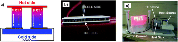 | ||
| Fig. 2 (a) Schematic of thermoelectric power generation; (b) a typical thermoelectric device; and (c) an example demonstration of thermoelectric power generation. | ||
A typical thermoelectric device is shown in Fig. 2(b). Modern devices consist of many legs of alternating n-type and p-type materials, allowing a current to flow through each leg sequentially while heat flows through each leg in parallel. For power generation applications, modules are subjected to a temperature gradient over the length of the legs and connected to a circuit, as in Fig. 2(c). Here a commercial thermoelectric module is subjected to a temperature difference using a flame as a heat source and a large aluminum block as the cold side heat sink. The imposed temperature gradient creates an electrochemical potential difference between the hot side and the cold side of the thermoelectric material which drives a current around the circuit, lighting up the LEDs.
Thermoelectrics can also be used as solid-state refrigerators or heat pumps by driving a current in a circuit with two dissimilar materials. This mode exploits the Peltier effect, discovered by Jean-Charles Peltier in 1834, where heat is absorbed or rejected at the interface of two dissimilar materials when a current is injected around a circuit. This is explained by introducing the Peltier coefficient, which is a material dependent parameter that is related to the Seebeck coefficient and which describes how much thermal energy is carried per charge carrier. Since the heat current must be continuous across the interface of two materials, if the materials have different Peltier coefficients heat will be either rejected or absorbed at the interface, depending on the sign of the difference between the Peltier coefficients and the direction of the current. If the current is injected in one direction the junction will extract heat,1,2,29 which is the basis for thermoelectric refrigeration; a current in the other direction will produce heat at the junction, and the device is acting as a heat pump. Usually the two materials are chosen to be thermoelectric materials with the opposite majority carrier (one n-type leg and one p-type leg) to maximize the difference between the Peltier coefficients and hence the amount of heat absorbed or generated.
III. Thermoelectric materials
Materials which are able to efficiently generate power using the Seebeck effect or refrigerate using the Peltier effect are known as thermoelectric materials. We would like a way to determine whether a given material will be a good thermoelectric material based on its properties. We can make educated guesses as to which properties will be important based on intuition: since the material has to pass electrical current in both the power generation and refrigeration mode we expect to need a material with high electrical conductivity. Since we want a large voltage to be generated per unit temperature gradient a large Seebeck coefficient is important. Finally, as we need to be able to maintain a temperature difference across the material, it seems reasonable to look for materials that also have low thermal conductivity. A simple heat transfer analysis yields the dimensionless parameter we seek, which is denoted ZT: | (1) |
After much experimentation, it was eventually determined that alloyed semiconductors with high carrier concentration are the most efficient bulk thermoelectric materials.31 The high carrier concentration allows for a good electrical conductivity, and the electrical properties can be optimized by varying the carrier concentration. Alloying disrupts the transport of phonons (quantized lattice vibrations which carry heat), resulting in a reduced thermal conductivity. The lattice thermal conductivity can be further reduced by using heavy elements with low sound velocities, such as Bi, Te, and Pb. Examples of commercial thermoelectric materials are Bi2Te3 and alloys such as BixSb2−xTe3 at room temperature, PbTe and alloys such as PbTe–PbSe at moderate temperature, and the alloy Si80Ge20 at high temperature.
Despite having multiple parameters to adjust, optimizing all the parameters together turns out to be very difficult because the properties are interdependent. For example, if we find the electrical conductivity is too low, we might want to increase the carrier concentration. However, while increasing the carrier concentration will increase the electrical conductivity, it will also decrease the Seebeck coefficient and increase the electronic contribution to the thermal conductivity. From Eqn 1, we see that these changes in properties will most likely not lead to a net increase in ZT, since any favorable change in one property is accompanied by an unfavorable change in the other properties. These conflicting trends are illustrated in Fig. 3 for n-type Si80Ge20. This type of dilemma caused the maximum ZT of any thermoelectric material to remain at ZT ≈ 1 for almost fifty years.
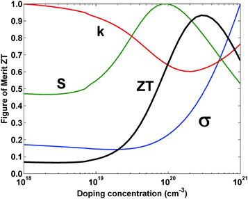 | ||
| Fig. 3 Normalized thermoelectric properties and ZTversus doping concentration at 300 K for n-type Si80Ge20. Curves are calculated from a numerical model developed by the authors. In the figure k refers to thermal conductivity, S refers to the Seebeck coefficient, and σ refers to the electrical conductivity. | ||
IV. Nanostructured materials
There have been two primary approaches taken to overcome these challenges. The first approach focuses on creating new materials: researchers try to synthesize complex solid solutions which have the desired properties. These materials have very complex crystal structures which can exhibit a low lattice thermal conductivity. An excellent review on this approach was recently published.27The other approach, which is the focus of this review, is to create nanostructured materials. By using the same materials but in a nanostructured form, it is possible to modify thermoelectric properties in ways that are not possible with bulk materials, which can lead to an enhancement in ZT.6,18,22,32–34
The idea of selectively modifying material properties using lower dimensional structures was introduced by Hicks and Dresselhaus in 1993.22 They theoretically showed that by using two-, one-, or even zero-dimensional structures one could obtain significant increases in electronic properties, far beyond what was believed possible in bulk materials. Others later theoretically showed a significant reduction in lattice thermal conductivity is possible by using nanostructures.33,34 Stimulated by these predictions, researchers were able to fabricate nanostructures such as superlattices (2D structures), nanowires (1D structures), and quantum dots (0D structures), forming thin-film materials for which thermoelectric properties could be measured. Soon thereafter, high ZTs were reported in a thin-film superlattice14 and a quantum dot superlattice.15Silicon nanowires were also reported to have a high ZT.16,17 All of these materials exhibited a decrease in lattice thermal conductivity. Others have reported that another type of nanostructure consisting of In0.53Ga0.47As with embedded ErAs nanoparticles can have a very low thermal conductivity below that of the corresponding bulk alloy.35 These researchers have also tried to use these particles to increase the Seebeck coefficient by filtering out low energy electrons,36 but a net increase in ZT from this method has not been confirmed.
These reports of enhanced ZT on thin film structures and nanowires have demonstrated the principle of nanostructuring to enhance ZT, although questions linger regarding the accuracy of the ZT reported due to experimental difficulties in measuring the properties accurately. However, even if these results can be confirmed, materials fabricated by atomic layer deposition techniques are not easily incorporated into commercial devices because they are slow and expensive to fabricate, and they cannot be fabricated in sufficient quantities. Fortunately, theoretical results obtained from studying superlattices provided a solution to this dilemma. Modeling of phonon transport in superlattices indicated that the primary benefit from nanostructures, a reduced lattice thermal conductivity, does not require an atomically perfect interface or an exact geometry.34 All that is required is a material with a high density of interfaces, which can be present in any geometry.37 This discovery led to the idea of a nanocomposite, which retains the high density of interfaces but does not have a special geometry or structure, significantly simplifying the fabrication process and allowing the material to be produced in large quantities.38 A nanocomposite is thus a type of bulk nanostructured material and will be the focus of this review.
V. Nanocomposites
A. Concept
The term “nanocomposite” has been used to describe several different types of structures. The original concept was for either nanoparticles embedded in a host or a heterostructure geometry with nanoparticles of different materials adjacent to each other.38,39 For the heterostructure geometry, when the two materials are the same the nanocomposite is essentially a material with nanometer sized grains. A TEM image of a typical Si80Ge20 nanocomposite20 is shown in Fig. 4. From the scale bars we can see that the grain size is only ten or twenty nanometers, much smaller than a typical Si80Ge20 grain size of one micron and larger.40–42 Because these nanostructures have a size smaller than the phonon mean free path but greater than the electron or hole mean free path, phonons are more strongly scattered by the interfaces than are electrons or holes, resulting in a net increase in ZT.![(a) TEM and (b) HRTEM images of a Si80Ge20 nanocomposite (from Ref. [20]).](/image/article/2009/EE/b822664b/b822664b-f4.gif)
As might be expected, because nanocomposites are not formed by atomic layer deposition methods, they are significantly quicker and cheaper to fabricate than superlattices or other nanostructures, yet retain the same enhancements in thermoelectric properties. The nanocomposite concept has been validated in several material systems: an increase in ZT for n-type Si80Ge20,20 p-type Si80Ge20,21 and p-type BixSb2−xTe318,19 has been experimentally demonstrated. Perhaps more importantly, the BixSb2−xTe3 nanocomposite was able to be incorporated into a macroscale device with record performance.18
B. Fabrication
When the nanocomposite concept was still being developed, nanostructured materials which exhibited enhanced thermoelectric properties had only been created using atomic layer deposition techniques, and it was unclear whether any bulk process could create a thermodynamically stable, nanostructured material with an improved figure of merit. The first challenge is to create a material with nanoscale structures throughout using only a bulk process. While several techniques are available to create nanoparticles,43,44 combining the nanoparticles into a fully dense solid is not as straightforward. Once the bulk material has been fabricated, the next challenge is to adjust the fabrication conditions so that the figure of merit is improved. This is more difficult because the effects of the fabrication conditions on the nanostructures formed and the material's thermoelectric properties are not always clear. A still unresolved question is why certain nanostructured materials exhibit improved properties while others do not. Some fabrication methods, while capable of creating a nanostructured material, cannot produce a material with an improved ZT no matter how the fabrication conditions are adjusted.The final challenge is to produce a thermodynamically stable material which can retain its nanoscale structures while being used in a practical device. If the nanostructures spontaneously dissolve during the course of operation the thermoelectric properties will return to those of the bulk material, removing any increase in efficiency that the nanostructured material was supposed to give. Creating a thermodynamically stable nanostructured material is difficult because the nanostructured form is not an equilibrium state of the material. Diffusion and energies associated with interfaces often act to remove nanoscale structures or variations in composition; in PbTe, for example, nanosized grains are not stable at elevated temperatures due to their high surface energy. Since in practice thermoelectrics must operate for years at high temperatures to maximize thermodynamic efficiency, thermal stability of nanostructured materials is an important issue and is a topic of ongoing research.
Despite these difficulties, several bulk processes have been developed in recent years which have successfully created stable nanocomposites with improved properties over those of their bulk counterparts. One method uses ball milling and hot pressing to create nanograined materials. In this technique, raw component elements, such as Bi and Te or Si and Ge, are ground into a nano-particle dust using a ball milling machine. The resulting mixture is then hot pressed at an appropriate temperature and pressure. If the pressing temperature and duration are adjusted correctly, the nanoparticles will fuse together but leave the interface between each particle intact, creating a fully dense solid material with nanosize grains, as shown in Fig. 4. This technique has been successfully implemented on n-type Si80Ge20,20 p-type Si80Ge20,21 and different types of BixSb2−xTe3.18,19 The advantages of this method are that it is simple and inexpensive to fabricate the materials, and the technique can be applied to any material system.
Another method to create a bulk nanocomposite is to use thermal processing techniques to induce the formation of nanoscale precipitates, an approach which has been successfully used by the Kanatzidis group in several material systems.23,24,45,46 By choosing the appropriate compounds and subjecting the material to a thermal processing procedure, a metastable solid solution of different elements can be made to undergo spinodal decomposition or nucleation and growth mechanisms to create nanoscale features.24 A related technique, known as matrix encapsulation, uses the fact that some materials are soluble in others in the liquid state but not in the solid state. By rapidly cooling the liquid mixture, the insoluble minority phase will precipitate, forming nanoparticles embedded in the host phase.45
These techniques have been applied with considerable success to several different solid solutions. High ZTs have been reported in n-type AgPbTe2/PbTe,46 n-type Pb1−xSnxTe/PbS,24 and p-type Na1−xPbmSbyTem+2.23 All of these materials achieved their high ZT values by exhibiting a markedly reduced thermal conductivity. To give an idea of the magnitude of the reduction, bulk PbTe has a thermal conductivity of about 2.4 W m−1K−1 at 300 K, while PbTe with two percent Sb that is matrix encapsulated has a thermal conductivity of about 0.8 W m−1K−1, a remarkable decrease.
VI. Challenges in understanding carrier transport
Nanocomposites have been successful in increasing ZT by reducing the thermal conductivity below that of the bulk material while allowing for large scale, quick, and inexpensive fabrication. The first generation of nanocomposites has been developed, and efforts to use the materials in commercial devices are currently under way. However, as discussed in the introduction, developing the second generation of nanocomposites will require a more controlled design process where the thermoelectric properties of different nanostructures can be predicted and the desired structure created using a bulk procedure. The current design process of trial and error will not be sufficient. This goal can only be achieved with a fundamental understanding of transport in these complex materials and how their nanoscale structure affects bulk properties.In the next section we discuss the difficulties in analyzing carrier transport in nanocomposites and what research is taking place to address these difficulties. While most of our discussion is focused on scattering processes caused by grain boundaries, it is important to note that as the grains become smaller and smaller the volume fraction of grain boundaries becomes comparable to the volume fraction of the material itself, making the grain boundaries essentially another phase inside a host material. The properties of the overall material are determined not just by scattering processes but by the presence of the grain boundary phase. Since the properties and composition of the grain boundary are almost completely unknown and not easily determined, transport in nanocomposites is usually explained in terms of grain boundary scattering processes, which is the approach we will follow. This dilemma already illustrates how much is unknown about carrier transport in nanocomposites.
A. Phonon transport
Since most nanocomposites to date have achieved their high ZT values by a reduction in lattice thermal conductivity (in this section just termed “thermal conductivity”), one might expect that phonon transport in nanocomposites is fairly well understood. However, the situation turns out to be just the opposite. Even in bulk materials, there is much uncertainty regarding the values of key quantities such as the phonon mean free path. Furthermore, the precise way in which interfaces affect phonon transport to reduce thermal conductivity in nanocomposites remains poorly understood. Theoretical predictions for the lower limit of thermal conductivity in nanostructured materials also turn out to be wrong, as was experimentally demonstrated by Cahill.47 This physical understanding is crucial to further reducing the thermal conductivity, however, and so here we highlight what is known about phonon transport and what we seek to understand.First, let us discuss what is known. Nanocomposites have shown that they are able to achieve a thermal conductivity lower than that of their bulk counterparts. Before the creation of nanostructured materials it was believed that the lower limit to the thermal conductivity was set by the value obtained by an alloy, as in Si1−xGex, and this lower value of the thermal conductivity was termed the “alloy limit.” While this “limit” remained for fifty years, recently nanocomposites have exhibited a lower thermal conductivity than that of their corresponding alloy.20,21 Why is this possible?
The reason is now fairly well understood. Phonons in a material have a spectrum of wavelengths, and phonons with different wavelengths contribute different amounts to the total thermal conductivity. Introducing the alloyed phase causes short wavelength phonons to be strongly scattered by impurity atoms, while mid- to long-wavelength phonons are less affected. This scattering process is very similar to Rayleigh scattering, where short wavelength light (high frequency blue light) is scattered preferentially by atmospheric molecules. Thus while short wavelength phonons are strongly scattered in alloys, mid- to long-wavelength phonons are still able to transport heat. Furthermore, it was shown previously that in bulk Si these mid- to long-wavelength modes can actually carry a substantial fraction of the heat.48 By incorporating structures with a larger characteristic length than that of an impurity atom, an interface scattering mechanism is introduced which scatters mid- to long-wavelength phonons, resulting in a further reduced thermal conductivity that is lower than the alloy limit.
This physical picture gives a good qualitative understanding of why nanocomposites are able to beat the alloy limit. Simple phonon models based on the Callaway model of thermal conductivity,49,50 which uses the Debye model, along with an additional interface scattering term have been able to explain thermal conductivity data for In0.53Ga0.47As/ErAs nanostructures35 and Si nanowires.16 However, while these models can fit the data by adjusting various fitting parameters, a more careful examination shows that many of the model's fundamental predictions are not correct. Figs. 5(a) and 5(b) show the cumulative distribution function of thermal conductivity with respect to phonon wavelength and mean free path for the Callaway model and a more exact molecular dynamics simulation48 in bulk, undoped Si at 300 K. From here we see that while the simple Callaway model can be adjusted to give the correct total thermal conductivity, the more quantitative results, such as phonon mean free path and wavelength, are not consistent even for the bulk case; in this case the spectral dependence of the thermal conductivity has only fair agreement with the molecular dynamics result, while the mean free path accumulation does not agree well. Crucially, the key result that long mean free path phonons carry a large fraction of the heat in undoped Si, which is an important fact to know when designing thermoelectric materials, is not predicted by the Callaway model. Thus even phonon transport in bulk materials is not well understood, and new discoveries are still taking place; Morelli et al. recently reported an unusually low thermal conductivity in bulk cubic AgSbTe2 due to extremely anharmonic bonds.51
![Cumulative distribution function of lattice thermal conductivity with respect to (a) phonon wavelength and (b) phonon mean free path predicted by the Callaway model and molecular dynamics simulations (Ref. [48]) in bulk, undoped Si at 300 K.](/image/article/2009/EE/b822664b/b822664b-f5.gif) | ||
| Fig. 5 Cumulative distribution function of lattice thermal conductivity with respect to (a) phonon wavelength and (b) phonon mean free path predicted by the Callaway model and molecular dynamics simulations (Ref. [48]) in bulk, undoped Si at 300 K. | ||
Nanocomposites add another layer of complexity to this problem because they contain many interfaces with a spacing smaller than the phonon mean free path, which introduces a thermal boundary resistance between different regions of the nanocomposite. While researchers have been able to use thermal boundary resistance to obtain a low thermal conductivity, there is currently limited ability to predict the thermal boundary resistance despite many years of research.52,53 Thermal boundary resistance has also been identified as the key mechanism for the low thermal conductivity in superlattices, rather than the periodicity of the superlattices.54–56 Such understanding led to the concept of a nanocomposite. Efforts have been made to calculate thermal boundary resistance using the Boltzmann equation57 and Monte Carlo simulations,58 and Minnich and Chen introduced a modified theory to analytically compute the thermal conductivity of nanocomposites.59
However, existing models cannot give an accurate prediction for the phonon transmissivity at a single interface, a fundamental parameter in predicting thermal boundary resistance. Nanoparticles inside the composites have multiple interfaces, raising questions about phonon scattering by these particles. In the past, scattering models based on Rayleigh scattering35 and acoustic Mie scattering theory60 have been used to treat nanoparticle scattering. These models, however, do not include interfacial roughness effects and the effects of scattering inside the particle. Although molecular dynamics61 may be a potential tool, available computation power at this stage limits the size of the nanoparticles that can be treated.
As discussed in the introduction to this section, this lack of understanding affects our ability to design and optimize nanostructured materials to have low thermal conductivity. For example, we are currently unable to answer questions such as which phonon modes are the dominant heat carriers in nanocomposites, what is the optimal size distribution of nanostructures, what type of interface leads to the strongest phonon scattering, or what is the interfacial resistance and reflectivity of a nanocomposite interface. In fact, it is not even clear what is the lower limit to the thermal conductivity in a nanostructure. For bulk materials, the criterion that the phonon mean free path must be at least half the phonon wavelength62,63 sets the lower limit. This might not be the case in nanostructured materials, however. Chen has suggested that the minimum thermal conductivity in nanostructures is likely lower than in bulk materials because the minimum thermal conductivity theory for bulk materials is based on isotropic scattering, while in nanostructures, interfacial scattering is highly anisotropic.34 Cahill has experimentally demonstrated that the thermal conductivity of layered WSe2 is six times lower than the value predicted by theory and only twice that of air, an experimental verification that nanostructures can affect phonon transport in ways that are not accounted for by current theories.47
It is clear there are many unanswered questions in phonon transport that critically affect how we design nanostructured materials to exhibit reduced thermal conductivity. Gaining a better understanding of the fundamentals of phonon transport in nanostructured materials is thus a key challenge. Despite the difficulties, some progress is being made, especially in theoretical analysis. Mingo and coworkers have used the non-equilibrium Green's function formalism for phonons64 to model phonon transport through nanotubes with defects, allowing the thermal conductivity to be calculated without any adjustable parameters.65 Molecular dynamics simulations are also being used to study phonon transport.66 Lukes and coworkers have employed this technique to calculate the thermal conductivity of various nanostructures,67–69 and Henry and Chen were able to extract phonon relaxation times in bulk Si from molecular dynamics calculations.48 Experimentally, Cahill was able to probe different parts of the phonon distribution by using a variable frequency time-domain thermoreflectance technique.70
These modeling and experimental efforts which help reveal the fundamental physics of phonon transport are key to further reducing the thermal conductivity. There is much work to be done, but it is expected that with a better understanding of phonon transport, further lattice thermal conductivity reductions should be possible.
B. Electronic transport
While we showed in the last section that the details of phonon transport are not well understood, researchers have nevertheless been able to engineer materials with low thermal conductivity based on a qualitative understanding. Unfortunately, this is not the case for electronic transport. In this case, the details of electronic transport in nanocomposites are not well understood, and only very few improvements in electronic properties have ever been achieved in either bulk or nanocomposite materials. This is a serious problem because creating the second generation of nanocomposites will most likely require some type of improvement in electronic properties.As in the case of phonons, the details of electron transport in both bulk and nanocomposite materials are extremely complex, and the usual theories often cannot be used to answer fundamental questions. The primary difficulty is that many of the characteristic lengths in both the bulk and nanocomposite material are smaller than the electron de Broglie wavelength, meaning that the standard analysis using the Boltzmann equation may not give accurate results.71,72 Some of these important length scales are illustrated in Fig. 6 for heavily doped bulk Si80Ge20, which shows a TEM image of a Si80Ge20 nanocomposite with numerically calculated length scales. The calculations show that in Si80Ge20 the electron wavelength is around five to ten nanometers, which is comparable to the grain size of ten to twenty nanometers, much larger than the inter-impurity distance of one to two nanometers, and longer than the electron's own mean free path, which is around two to five nanometers! This results in difficulties for theoretical analysis because the use of the Boltzmann equation requires that the mean free path be much larger than the wavelength, and as a result some predictions from the Boltzmann equation may not be correct, as was the case with the Callaway model for phonons. The prediction of the wavelength being longer than the mean free path may also be caused by the inaccuracy of scattering models, which are mostly derived assuming that the doping level is not too high. Thermoelectric materials are very highly doped and are usually degenerate, however, and their electrical properties are sometimes closer to those of metals than semiconductors. Hence, more careful examination of electron transport in bulk materials is needed.
![A TEM image (Ref. [20]) of a heavily doped Si80Ge20 nanocomposite along with some important numerically calculated characteristic lengths.](/image/article/2009/EE/b822664b/b822664b-f6.gif) | ||
| Fig. 6 A TEM image (Ref. [20]) of a heavily doped Si80Ge20 nanocomposite along with some important numerically calculated characteristic lengths. | ||
In addition to these difficulties, electron transport in nanocomposites is affected by the presence of the interfaces, in many cases significantly. In fact, for many years it was believed that nanocomposites could not exhibit enhanced ZT because of a large reduction in electrical conductivity caused by electron interface scattering.42,73 It was eventually realized that to minimize interfacial scattering of electrons, materials with similar band structures, or even the same material, should be used to reduce the bandedge offset.41 We now know that this strategy works because ZT enhancements have been demonstrated in nanograined n-type20 and p-type21Si80Ge20. However, both of these materials show a reduction in electrical conductivity, and it is difficult to determine how to minimize this reduction based on a simple qualitative understanding.
Clearly much remains unknown about electronic transport in nanocomposites, but if nanocomposites are ever to achieve an improvement in electrical properties, the details of the transport processes must be better understood. The focus of the current research is on modeling electronic transport with more sophisticated formalisms. While almost all analyses of transport in semiconductors use the Boltzmann equation in some form,42,71,74 modeling transport in nanocomposites will require more powerful tools such as non-equilibrium Green's functions, which explicitly take account of electron wave effects. Exactly how to use these methods is still being investigated because detailed results require detailed information about the structure of a nanocomposite grain boundary which is not currently available. Research in this field is only just beginning, and it will most likely take some time before a clearer picture of electron transport in nanocomposites emerges.
VII. Strategies for the next generation of nanocomposites
While the last section showed that there is much to be understood about phonon and electronic transport in nanocomposites, this also means that there is still much room for innovation and improvement. Since the lattice thermal conductivity in nanocomposites has already been reduced, further improved materials will most likely feature some type of improvement in electrical properties combined with a reduction in lattice thermal conductivity. In the final section, we discuss several strategies to improve electrical properties which might be used in the next generation of nanocomposite thermoelectric materials.A. Increasing the mobility
The first way in which electrical properties could be improved is simply by reducing the impact of grain boundaries on electron transport. The predominant model for the grain boundary region predicts that grain boundaries should have a minor effect on the mobility at high doping levels,75–77 but in practice the mobility is often substantially reduced. This is illustrated in Fig. 7, which shows the experimental electron mobility of heavily doped nanostructured n-type Si80Ge20 along with a theoretical calculation for a bulk material at the same doping level. The experimental mobility is about forty percent lower than the theoretical expectation at room temperature, meaning that if the mobility could be restored to closer to the theoretical value, ZT could be increased by up to forty percent for this case. Our group is currently investigating this problem by examining the microstructure of our nanocomposite samples and modeling carrier transport with grain boundary scattering models. We hope that by gaining a better understanding of the electron scattering process at grain boundaries we will be able to modify the fabrication process to produce materials with a minimum reduction in mobility.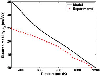 | ||
| Fig. 7 Theoretical prediction and experimental results for the mobility of n-type nano-Si80Ge20. Results from measurements and calculations by the authors. | ||
The Kanatzidis group recently made progress towards this goal with the introduction of “synergistic nanostructuring.”26 They found that nanostructured PbTe with encapsulated nanodots made of both Pb and Sb has an increased mobility over that of the bulk PbTe, resulting in a ZT a factor of two larger than that of bulk PbTe. This increase in mobility only occurs when both Pb and Sb are present together in the nanoparticle. So far there has been no explanation for this effect, but their result gives hope that a similar effect is possible in other material systems.
B. Energy filtering
While the previous section showed that grain boundaries can negatively affect the mobility, it is also possible for grain boundaries to play a positive role through energy filtering. The concept of energy filtering can be understood from Fig. 8, which shows the calculated normalized Seebeck distribution versus energy for heavily doped bulk n-type Si80Ge20. The Seebeck coefficient is proportional to the integral of this curve. From here we see that low energy electrons actually reduce the Seebeck coefficient because this portion of the Seebeck distribution is negative. This suggests a strategy, which is termed energy filtering, whereby an additional scattering mechanism is introduced which preferentially scatters low energy electrons, minimizing their contribution to transport properties and thus increasing the Seebeck coefficient. In nanocomposites, the obvious scattering mechanism is electron grain boundary scattering, which does reduce the mobility but also preferentially scatters electrons with energies less than the barrier height. Energy filtering has been investigated theoretically78 and experimentally by Shakouri and coworkers, who reported that a InGaAs/InGaAlAs superlattice exhibited an increase in power factor S2σ due to energy filtering effects.36 Increases in the Seebeck coefficient due to energy filtering in bulk nanostructured PbTe-based materials have also been reported, though the mobility was adversely affected.79,80 If a bulk fabrication process can be found which minimizes the degredation of the mobility while enhancing the Seebeck coefficient, the resulting material would have a net increase in power factor. This method is a good example of how nanostructuring can be used to improve electrical properties while still maintaining a low thermal conductivity.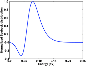 | ||
| Fig. 8 Calculated normalized Seebeck distribution versus energy for heavily doped bulk n-type Si80Ge20. Low energy electrons reduce the total Seebeck coefficient. Result from a numerical model developed by the authors. | ||
C. Resonant levels to enhance the density of states
A recent result which has resulted in a remarkable increase in ZT is the use of impurity band energy levels to increase the Seebeck coefficient.25 In most semiconductors, the addition of impurity atoms introduces states with energies in the band gap. If these states are very close to the conduction or valence band edges, as is the case for P or B in Si, the electrons (or holes) will be thermally activated into the conduction (or valence) bands and will be able to conduct. In some exceptional cases, however, the energy level created by the impurity can actually lie in the conduction or valence bands, creating a resonant level and a local maximum in the electronic density of states. This is qualitatively illustrated in Fig. 9. If the Fermi level is close to the distortion, it is theoretically expected that the Seebeck coefficient will increase. Enhancements in thermoelectric properties due to an increase in the electronic density of states were previously theoretically predicted by Mahan81 and Dresselhaus.22 Recently, an increase in Seebeck coefficient using the resonant level concept was experimentally demonstrated by Heremans and coworkers in bulk Tl-doped PbTe.25Tl introduces a resonant level near the valence band edge in PbTe, and since the Fermi level in p-type PbTe is also near the valence band edge the Seebeck coefficient increases significantly over that of the bulk. Just by introducing a small Tl concentration, these researchers were able to double ZT from ZT = 0.7 for bulk p-type PbTe to ZT = 1.5 for 2% Tl-doped PbTe.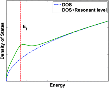 | ||
| Fig. 9 Schematic of the effect of a resonant level on the electronic density of states (DOS). | ||
It should be possible to create a material which uses both the resonant level and the nanocomposite concepts: one simply needs to add Tl to PbTe and generate the nanocomposite in the usual manner. The resulting material should have a lower thermal conductivity than the bulk value but significantly improved electrical properties due to the Tl doping. Our group has already started experimenting with this idea, and we have found that by simply mixing together Pb, Te, and Tl in the right proportions we are able to reproduce Heremans' result. We are currently working to stabilize the resulting nanocomposite, since small grains in PbTe tend to grow even at moderate temperatures. If grain stabilization can be achieved it is expected that the material will have a further improved ZT value.
The other area of research that suggests itself from this work is identifying other material systems in which the resonant level concept would be effective. While Tl-doped PbTe did show a remarkable increase in ZT, Tl itself is highly toxic, making the commercial use of this material undesirable. Though resonant levels are not common, it is reasonable to believe that there are at least a few other materials in which impurities can introduce resonant levels near the band edges. These might be able to be identified using density functional theory or spectroscopic techniques to determine the impurity energy levels. These techniques together will hopefully help clarify the origin of the resonant level and allow researchers to fully realize the potential of this approach towards both enhancing the power factor and reducing the thermal conductivity.
D. Reducing the bipolar effect
The major theme of nanocomposites has been a reduction of the lattice thermal conductivity. However, nanocomposites now have such a low lattice thermal conductivity that the other contributions to the thermal conductivity, the electronic thermal conductivity and the bipolar thermal conductivity, can be comparable in magnitude. This is illustrated in Fig. 10, which shows the calculated temperature dependence of the total, lattice, electronic, and bipolar thermal conductivities for heavily doped bulk n-type Si80Ge20. In this case the electronic thermal conductivity can account for almost 50% of the total thermal conductivity! While the bipolar thermal conductivity is not as large, often it can be a significant contribution to the thermal conductivity at high temperature, as is the case in Fig. 11(b). Here we focus on strategies to reduce the bipolar contribution; the final section will focus on the electronic contribution.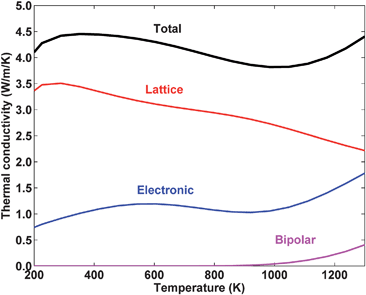 | ||
| Fig. 10 The calculated temperature dependence of the total, lattice, electronic, and bipolar thermal conductivities for heavily doped bulk n-type Si80Ge20. Results from a numerical model developed by the authors. | ||
![(a) Measured power factor and (b) measured thermal conductivity of a BixSb2−xTe3 nanocomposite (data from Ref. [18]). The solid lines are to guide the eye. The power factor of the nanocomposite is higher at elevated temperatures, and the reduced slope of the thermal conductivity for the nanocomposite case at high temperature indicates a reduced bipolar contribution.](/image/article/2009/EE/b822664b/b822664b-f11.gif) | ||
| Fig. 11 (a) Measured power factor and (b) measured thermal conductivity of a BixSb2−xTe3 nanocomposite (data from Ref. [18]). The solid lines are to guide the eye. The power factor of the nanocomposite is higher at elevated temperatures, and the reduced slope of the thermal conductivity for the nanocomposite case at high temperature indicates a reduced bipolar contribution. | ||
The bipolar effect is due to the fact that there are two types of carriers, electrons and holes. At high temperature many electrons are thermally excited from the valence band to the conduction band, leaving behind an equal number of holes. The presence of these two types of carriers allows heat conduction to take place even if the net electrical current is zero.1 Furthermore, since electrons and holes have opposite charges, the Seebeck coefficient is significantly suppressed if both electrons and holes are present. Thus reducing the bipolar effect can improve the figure of merit in two ways. While many thermoelectric materials are usually so highly doped that this effect is not strong, for some materials at elevated temperature the bipolar thermal conductivity can be a significant component of the total thermal conductivity and the Seebeck coefficient can be markedly reduced.
Clearly the way to reduce the bipolar effect is to somehow affect the minority carrier but not the majority carrier. But how can this be accomplished if the equilibrium concentrations of electrons and holes are an intrinsic property of the material? One way is to create a nanostructure which preferentially scatters minority carriers. A reduced bipolar effect was observed in a BixSb2−xTe3 nanocomposite alloy,18 and modeling indicates that the electrons in p-type BixSb2−xTe3 are more strongly scattered by the grain boundaries than the holes, resulting in a decreased electron contribution to the transport properties. As seen in Fig. 11(a) and 11(b), this approach increases the power factor S2σ in addition to maintaining a low total thermal conductivity, especially at high temperatures. This is why the BixSb2−xTe3 nanocomposite is able to retain its high figure of merit over the entire temperature range.
The reason why electrons are preferentially scattered, however, is currently not understood. Further enhancing this preferential scattering requires detailed knowledge of the electron and hole scattering processes at grain boundaries in BixSb2−xTe3, similar to that required to minimize the mobility reduction in nanocomposites discussed previously. If this technique can be better understood and improved, it will be a powerful way to maintain a high ZT at elevated temperatures.
E. Reducing the electronic thermal conductivity
The final strategy we consider to enhance ZT is reducing the electronic thermal conductivity. At first, it might seem impossible to reduce the thermal conductivity from electrons or holes: after all, charge carriers must travel through the thermoelectric material, and when they do so they will inevitably carry heat. This idea is embodied in the Wiedemann–Franz law,29 which states that the electronic thermal conductivity ke and electrical conductivity σ in a metal or degenerate semiconductor are related as:| ke = LσT | (2) |
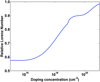 | ||
| Fig. 12 The calculated Lorenz number, relative to the theoretical value L = 2.45 × 10⁻⁸ W Ω K−2, versus doping concentration for Si at 300 K. The Lorenz number approaches the theoretical value as the semiconductor becomes degenerate. Result from a numerical model developed by the authors. | ||
It has been theoretically shown that in certain cases the Wiedemann–Franz law is violated and the Lorenz number is much smaller than its normal value, leading to a reduced electronic contribution to the thermal conductivity. Let us discuss how this can happen. Mahan and Sofo first showed that materials with a certain electronic structure will have a reduced electronic thermal conductivity.81 Based on their analysis, it can be shown that if one could obtain a material with a very sharply peaked electronic density of states approaching a delta function, the electronic thermal conductivity will go to zero, violating the Wiedemann–Franz law. Humphrey and Linke82 later showed that a delta function density of states along with a particular inhomogeneous doping profile allows electrons to travel reversibly through a material, which is the most efficient electron transport that is possible to achieve. In this case ZT is only limited by the lattice thermal conductivity, and as this becomes small ZT essentially goes to infinity. This is made possible by a violation of the Wiedemann–Franz law.
To implement this strategy it is necessary to search for materials with very strongly peaked density of states near the Fermi level. Mahan and Sofo suggested materials in which atoms have tightly bound electronic f levels, such as YbAl3, as these f levels have a Lorentzian density of states. Another approach is to use quantum dots, as these zero-dimensional structures inherently only have states at certain specific energies, giving a delta function density of states. The challenge here is to create quantum dots with the correct energy levels and in bulk quantities.
Another way one could implement this strategy is to use the resonant level concept discussed earlier. The mechanism by which the Seebeck coefficient is enhanced is by a local maximum in the density of states contributed by the resonant level, which we now see is precisely the same mechanism which reduces the Lorenz number. If this effect could be enhanced we will obtain a simultaneous increase in Seebeck coefficient and reduction in electronic thermal conductivity, leading to a dramatic increase in ZT.
There are other ways to reduce the electronic thermal conductivity besides using an increase in the electronic density of states. Bian et al. showed that the Lorenz number in superlattices can be tuned by varying the doping concentration and layer thickness, and in some cases a fifty percent reduction in Lorenz number is possible.83
A completely unrelated way in which one could obtain a reduced Lorenz number is by using strongly correlated materials. In this case, the fundamental assumption that carriers are uncorrelated is not valid and so the Wiedemann–Franz law is not expected to hold. Moore and coworkers have shown that the Hubbard model can explain the high Seebeck coefficient for certain values of the doping level in NaxCoO2.84 Cases have been identified where the Wiedemann–Franz law is violated in molecular junctions.85,86 Additionally, an enormous Seebeck coefficient of −45000 µV K−1 and record high power factor have been reported in the strongly correlated semiconductor FeSb2 at 10 K.87 While some of these concepts might not be feasible to implement for practical thermoelectric devices, the results show that there are still many unexplored phenomena in strongly correlated materials which might prove beneficial.
This section showed that it should be possible to reduce the heat carried by electrons while not impeding the electrical conductivity, a very unintuitive prediction. Materials which implement these ideas will most likely not be available in the near future; currently there is no simple way even to measure the electronic thermal conductivity, let alone manipulate it or reduce it. However, research focusing on obtaining fundamental information on electron transport is ongoing, and there is a good chance that this research will lead to a successful implementation of one of these strategies.
VIII. Conclusions
This review has described the principles and current achievements of bulk nanostructured materials. These materials have experimentally demonstrated a higher ZT than that of their bulk counterparts by reducing the thermal conductivity to values lower than were previously thought possible. More importantly for practical use, the materials can be fabricated cheaply, quickly, and in a form that is compatible with existing thermoelectric device configurations. The first generation of bulk nanostructured materials is currently being commercialized, and we are optimistic that thermoelectric devices which use these materials will soon find more widespread applications. However, creating the second generation will require a fundamental understanding of carrier transport in these complex materials which is presently lacking. We have detailed the challenges and current research in understanding carrier transport and identified several possible research directions which might lead to the next generation of bulk nanostructured materials. We hope that further research in this field will allow thermoelectrics to play a positive role in any future energy solution.Acknowledgements
A.M. would like to acknowledge the support of the NDSEG Graduate Fellowship. The authors are grateful for the support of the Department of Energy (DE-FG02-87ER46516), NSF (CMMI-0833150 and CMMI-0833084), and the MIT Energy Initiative.References
- G. S. Nolas, J. Sharp, and H. Goldsmid, Thermoelectrics: Basic Principles and New Materials Developments, Springer, New York, 2001 Search PubMed.
- D. Rowe, ed., Thermoelectrics Handbook: Macro to Nano, CRC Press, Boca Raton, 2006 Search PubMed.
- T. M. Tritt and M. A. Subramanian, MRS Bull., 2006, 31, 188.
- T. M. Tritt, ed., Recent Trends in Thermoelectric Materials Research, in Semiconductors and Semimetals, Academic Press, San Diego, 2001, vol. 69–71 Search PubMed.
- G. Chen, M. S. Dresselhaus, G. Dresselhaus, J. P. Fleurial and T. Caillat, Int. Mater. Rev., 2003, 48, 45 Search PubMed.
- M. Dresselhaus, G. Chen, M. Y. Tang, R. G. Yang, H. Lee, D. Z. Wang, Z. F. Ren, J. P. Fleurial and P. Gogna, Adv. Mater., 2007, 19, 1043 CrossRef CAS.
- L. E. Bell, Science, 2008, 321, 1457 CrossRef CAS.
- J. Yang, in 24th International Conference on Thermoelectrics, 2005, pp. 170–174 Search PubMed.
- http://www.research.philips.com/newscenter/archive/2006/060227-woodstove.html. Accessed November 2008.
- H. Scherrer, L. Vikhor, B. Lenoir, A. Dauscher and P. Poinas, J. Power Sources, 2003, 115, 141 CrossRef CAS.
- H. Xi, L. Luo and G. Fraisse, Renewable Sustainable Energy Rev., 2007, 11, 923 CrossRef CAS.
- S. Maneewan, J. Hirunlabh, J. Khedari, B. Zeghmati and S. Teekasap, Sol. Energy, 2005, 78, 495 CrossRef CAS.
- S. Maneewan, J. Khedari, B. Zeghmati, J. Hirunlabh and J. Eakburanawat, Renewable Energy, 2004, 29, 743 CrossRef CAS.
- R. Venkatasubramanian, E. Siivola, T. Colpitts and B. O'Quinn, Nature, 2001, 413, 597 CrossRef CAS.
- T. C. Harman, P. J. Taylor, M. P. Walsh and B. E. LaForge, Science, 2002, 297, 2229 CrossRef CAS.
- A. I. Hochbaum, R. Chen, R. D. Delgado, W. Liang, E. C. Garnett, M. Najarian, A. Majumdar and P. Yang, Nature, 2008, 451, 163 CrossRef CAS.
- A. I. Boukai, Y. Bunimovich, J. Tahir-Kheli, J.-K. Yu, W. A. Goddard Iii and J. R. Heath, Nature, 2008, 451, 168 CrossRef CAS.
- B. Poudel, Q. Hao, Y. Ma, Y. Lan, A. Minnich, B. Yu, X. Yan, D. Wang, A. Muto, D. Vashaee, X. Chen, J. Liu, M. S. Dresselhaus, G. Chen and Z. Ren, Science, 2008, 320, 634 CrossRef CAS.
- Y. Ma, Q. Hao, B. Poudel, Y. Lan, B. Yu, D. Wang, G. Chen and Z. Ren, Nano Lett., 2008, 8, 2580 CrossRef CAS.
- X. W. Wang, H. Lee, Y. C. Lan, G. H. Zhu, G. Joshi, D. Z. Wang, J. Yang, A. J. Muto, M. Y. Tang, J. Klatsky, S. Song, M. S. Dresselhaus, G. Chen and Z. Ren, Appl. Phys. Lett., 2008, 93, 193121 CrossRef.
- G. Joshi, H. Lee, Y. Lan, X. Wang, G. Zhu, D. Wang, R. W. Gould, D. C. Cuff, M. Y. Tang, M. S. Dresselhaus, G. Chen and Z. Ren, Nano Lett., 2008, 8, 4670 CrossRef CAS.
- L. Hicks and M. Dresselhaus, Phys. Rev. B, 1993, 47, 16631 CrossRef CAS.
- P. F. P. Poudeu, J. D'Angelo, A. D. Downey, J. L. Short, T. P. Hogan and M. G. Kanatzidis, Angew. Chem., Int. Ed., 2006, 45, 3835 CrossRef CAS.
- J. Androulakis, C. H. Lin, H. J. Kong, C. Uher, C. I. Wu, T. Hogan, B. A. Cook, T. Caillat, K. M. Paraskevopoulos and M. G. Kanatzidis, J. Am. Chem. Soc., 2007, 129, 9780 CrossRef CAS.
- J. P. Heremans, V. Jovovic, E. S. Toberer, A. Saramat, K. Kurosaki, A. Charoenphakdee, S. Yamanaka and G. J. Snyder, Science, 2008, 321, 554 CrossRef CAS.
- J. Sootsman, H. Kong, C. Uher, J. D'Angelo, C. I. Wu, T. Hogan, T. Caillat and M. Kanatzidis, Angew. Chem., Int. Ed., 2008, 47, 8618 CrossRef CAS.
- G. J. Snyder and E. S. Toberer, Nat. Mater., 2008, 7, 105 CrossRef CAS.
- F. J. DiSalvo, Science, 1999, 285, 703 CrossRef CAS.
- G. Chen, Nanoscale Energy Transport and Conversion, Oxford University Press, New York, 2005 Search PubMed.
- G. Slack, in CRC Handbook of Thermoelectrics, ed. D. M. Rowe, CRC Press, Boca Raton, 1995, pp. 407–440 Search PubMed.
- A. Ioffe, Semiconductors Thermoelements and Thermoelectric Cooling, Infosearch Ltd., London, 1957 Search PubMed.
- G. Chen and A. Shakouri, J. Heat Transfer, 2002, 124, 242 CrossRef CAS.
- R. Venkatasubramanian, Recent Trends in Thermoelectric Materials Research III, in Semiconductors and Semimetals, Academic Press, 2001, vol. 71, pp. 175–201 Search PubMed.
- G. Chen, Recent Trends in Thermoelectric Materials Research III, in Semiconductors and Semimetals, Academic Press, 2001, vol. 71, pp. 203–259 Search PubMed.
- W. Kim, J. Zide, A. Gossard, D. Klenov, S. Stemmer, A. Shakouri and A. Majumdar, Phys. Rev. Lett., 2006, 96, 045901 CrossRef.
- J. M. O. Zide, D. Vashaee, Z. X. Bian, G. Zeng, J. E. Bowers, A. Shakouri and A. C. Gossard, Phys. Rev. B: Condens. Matter Mater. Phys., 2006, 74, 205335 CrossRef.
- M.-S. Jeng, R. Yang, D. Song and G. Chen, J. Heat Transfer, 2008, 130, 042410 CrossRef.
- R. Yang, G. Chen and M. Dresselhaus, Phys. Rev. B, 2005, 72, 125418 CrossRef.
- R. Yang, G. Chen and M. Dresselhaus, Nano Lett., 2005, 5, 1111 CrossRef CAS.
- D. M. Rowe, V. S. Shukla and N. Savvides, Nature, 1981, 290, 765 CrossRef CAS.
- D. M. Rowe, L. W. Fu and S. G. K. Williams, J. Appl. Phys., 1993, 73, 4683 CrossRef.
- C. B. Vining, J. Appl. Phys., 1991, 69, 331 CrossRef CAS.
- W. Wang, B. Poudel, J. Y. Huang, D. Z. Wang, S. Kunwar and Z. F. Ren, Nanotechnology, 2005, 16, 1126 CrossRef CAS.
- W. Wang, B. Poudel, J. Yang, D. Z. Wang and Z. F. Ren, J. Am. Chem. Soc., 2005, 127, 13792 CrossRef CAS.
- J. R. Sootsman, R. J. Pcionek, H. Kong, C. Uher and M. G. Kanatzidis, Chem. Mater., 2006, 18, 4993 CrossRef CAS.
- K. F. Hsu, S. Loo, F. Guo, W. Chen, J. S. Dyck, C. Uher, T. Hogan, E. K. Polychroniadis and M. G. Kanatzidis, Science, 2004, 303, 818 CrossRef CAS.
- C. Chiritescu, D. G. Cahill, N. Nguyen, D. Johnson, A. Bodapati, P. Keblinski and P. Zschack, Science, 2007, 315, 351 CrossRef CAS.
- A. S. Henry and G. Chen, J. Comput. Theor. Nanosci., 2008, 5, 141 CAS.
- J. Callaway, Phys. Rev., 1959, 113, 1046 CrossRef CAS.
- E. F. Steigmeier and B. Abeles, Phys. Rev., 1964, 136, A1149 CrossRef.
- D. T. Morelli, V. Jovovic and J. P. Heremans, Phys. Rev. Lett., 2008, 101, 035901 CrossRef CAS.
- P. Kapitza, J. Phys. (Moscow), 1941, 4, 181 Search PubMed.
- E. Schwartz and R. Pohl, Rev. Mod. Phys., 1989, 61, 605 CrossRef.
- G. Chen, Phys. Rev. B, 1998, 57, 14958 CrossRef CAS.
- G. Chen, J. Heat Transfer, 1997, 119, 220 CrossRef CAS.
- G. Chen and T. Zeng, Microscale Thermophys. Eng., 2001, 5, 71 Search PubMed.
- R. Prasher, Int. J. Heat Mass Transfer, 2005, 48, 4942 CrossRef CAS.
- H. Zhong and J. R. Lukes, Phys. Rev. B: Condens. Matter Mater. Phys., 2006, 74, 125403 CrossRef.
- A. Minnich and G. Chen, Appl. Phys. Lett., 2007, 91, 073105 CrossRef.
- A. Khitun, K. L. Wang and G. Chen, Nanotechnology, 2000, 11, 327 CrossRef CAS.
- Z. Neil and R. L. Jennifer, Phys. Rev. B: Condens. Matter Mater. Phys., 2008, 77, 094302 CrossRef.
- G. Slack, Solid State Phys., 1979, 34, 1 CAS.
- D. G. Cahill, S. K. Watson and R. O. Pohl, Phys. Rev. B, 1992, 46, 6131 CrossRef CAS.
- W. Zhang, T. S. Fisher and N. Mingo, Numer. Heat Transfer, Part B: Fundam., 2007, 51, 333 Search PubMed.
- N. Mingo, D. A. Stewart, D. A. Broido and D. Srivastava, Phys. Rev. B: Condens. Matter Mater. Phys., 2008, 77, 033418 CrossRef.
- A. McGaughey and M. Kaviany, in Advances in Heat Transfer, ed. G. A. Greene, J. P. Hartnett, and Y. I. Cho,Academic Press, New York, 2006, vol. 39, pp. 169–255 Search PubMed.
- Y. Chen, D. Li, J. R. Lukes, Z. Ni and M. Chen, Phys. Rev. B: Condens. Matter Mater. Phys., 2005, 72, 174302 CrossRef.
- C. Yunfei, L. Deyu, J. R. Lukes and A. Majumdar, J. Heat Transfer, 2005, 127, 1129 CrossRef.
- Y. Chen, D. Li, J. Yang, Y. Wu, J. R. Lukes and A. Majumdar, Phys. Rev. B: Condens. Matter, 2004, 349, 270 CAS.
- K. Yee Kan and G. C. David, Phys. Rev. B: Condens. Matter, 2007, 76, 075207 CrossRef.
- M. Lundstrom, Fundamentals of Carrier Transport, Cambridge University Press, Cambridge, 2000, 2nd edn Search PubMed.
- J. Singh, Physics of Semiconductors and their Heterostructures, McGraw-Hill, Singapore, 1996 Search PubMed.
- N. Scoville, C. Bajgar, J. Rolfe, J. Fleurial and J. Vandersande, Nanostruct. Mater., 1995, 5, 207 CrossRef CAS.
- D. L. Rode, Phys. Rev. B, 1970, 2, 1012 CrossRef.
- C. R. M. Grovenor, J. Phys. C: Solid State Phys., 1985, 18, 4079 CrossRef CAS.
- J. Y. W. Seto, J. Appl. Phys., 1975, 46, 5247 CrossRef CAS.
- T. I. Kamins, J. Appl. Phys., 1971, 42, 4357 CrossRef CAS.
- D. Vashaee and A. Shakouri, Phys. Rev. Lett., 2004, 92, 106103 CrossRef.
- J. P. Heremans, C. M. Thrush and D. T. Morelli, Phys. Rev. B, 2004, 70, 115334 CrossRef.
- J. P. Heremans, C. M. Thrush and D. T. Morelli, J. Appl. Phys., 2005, 98, 063703 CrossRef.
- G. D. Mahan and J. O. Sofo, Proc. Natl. Acad. Sci. U. S. A., 1996, 93, 7436 CrossRef CAS.
- T. E. Humphrey and H. Linke, Phys. Rev. Lett., 2005, 94, 096601 CrossRef CAS.
- Z. Bian, M. Zebarjadi, R. Singh, Y. Ezzahri, A. Shakouri, G. Zeng, J. H. Bahk, J. E. Bowers, J. M. O. Zide and A. C. Gossard, Phys. Rev. B: Condens. Matter Mater. Phys., 2007, 76, 205311 CrossRef.
- S. Mukerjee and J. E. Moore, Appl. Phys. Lett., 2007, 90, 112107 CrossRef.
- M. Padraig, M. Subroto and M. Joel, Phys. Rev. B: Condens. Matter Mater. Phys., 2008, 78, 161406 CrossRef.
- K. Bjorn, K. Jurgen and P. Jukka, Phys. Rev. Lett., 2008, 100, 066801 CrossRef.
- A. Bentien, S. Johnsen, G. K. H. Madsen, B. B. Iversen and F. Steglich, Europhys. Lett., 2007, 80, 17008 CrossRef.
| This journal is © The Royal Society of Chemistry 2009 |