Random walk numerical simulation for solar cell applications
Juan A.
Anta
Departamento de Sistemas Físicos, Químicos y Naturales, Universidad Pablo de Olavide, 41013, Sevilla, Spain
First published on 23rd February 2009
Abstract
Numerical modelling based on random walk methods provides a very versatile tool to describe transport and recombination processes in solar cells made with disordered materials and nanostructured devices. These methods are especially suited to describe these systems since they are characterized by a wide dispersion of spatial and energy states.
 Juan A. Anta Juan A. Anta | Juan A. Anta is an Assistant Professor at the University “Pablo de Olavide”, Seville, Spain. He obtained a BA in Chemistry from the Universidad Complutense of Madrid, Spain and carried out his PhD research at the Physical Chemistry Institute of the National Research Council of Spain. In 1997 and 1998 he was a postdoctoral fellow in the Department of Theoretical Chemistry at the University of Oxford and from mid-1999 to mid-2000 he was research assistant in the Department of Chemistry at Imperial College, London. His research focuses on solar cell modelling, computer simulation and nanostructured solar cells. |
Broader contextCurrent research into new architectures for low-cost photovoltaic devices based on disordered materials and the boom in nanotechnology provides new and exciting opportunities for computer simulation methods. This paper is concerned with the application of stochastic simulation methods in solar cell modelling involving disordered materials. Numerical modelling based on random walk methods provides a very versatile tool to describe transport and recombination processes in solar cells made with disordered materials. These methods are especially suited to describe these systems since they are characterized by a wide dispersion of spatial and energy states. This review includes an historical perspective, describes the basic features of these techniques and provides key references to state of the art research. |
Introduction
The use of electronic computing machines to simulate processes of physical interest is well established. Computer simulations have been widely utilized since the first large-scale computers were introduced during and after World War II. The Metropolis Algorithm1 was one of first algorithms to improve the capability of computers to perform large-scale numerical calculations. Computer simulation is also closely related historically to the use of stochastic procedures. The Monte Carlo method, based on the massive generation of random numbers, has been extensively applied in Nuclear Physics, Condensed-Matter Physics and Theoretical Chemistry.2 The Monte Carlo method takes advantage of the law of large numbers to avoid the calculation of huge multidimensional integrals, such as those associated with the basic laws of Quantum Physics and Statistical Mechanics. In general, Computer Simulation methods provide a way to replace the solution to a particularly difficult analytical or numerical problem by proposing a suitable algorithm. This algorithm is then fed to a computer so that the difficult numerical work is done by the machine. The work of the researcher is to design the computer “experiment”, i.e. to write the algorithm, and then to analyse the results so that valuable physical information can be obtained.Current research on new architectures for low-cost photovoltaic devices based on disordered materials and the boom in nanotechnology provides new exciting fields in which to apply computer simulation methods. This paper is concerned with the application of stochastic simulation methods in solar cell modelling involving disordered materials. It must be noted that two different terminologies are used in the literature: either Random Walk (RW) or Monte Carlo. Nevertheless both are based on the same principles and lead to the same conclusions. In the following we will use RW to refer to these numerical approaches.
The use of RW methods in disordered and nanostructured solar cells is especially appealing due to the key role of the interplay between transport and recombination. Adequate solar cell operation is based on a combination of good visible light harvesting, efficient charge separation, fast transport and slow recombination. In novel solar cells based on disordered materials, this fortunate combination is achieved by interpenetrating, in the nanoscale, an electron-conducting material with a hole-conducting one. In typical Dye Sensitised Solar Cells (DSSC)3 the first is a nanostructured semiconductor oxide and the second a liquid electrolyte. In plastic4 and bulk heterojunction solar cells5 charge separation is achieved by combining polymers and organic molecules with different conducting properties. In both kinds of solar cells disorder favours light harvesting (and decreases the fabrication costs) but contributes to a slow down of transport and enhances recombination. Hence, a good understanding of the transport and recombination properties of these materials (both for electrons and holes) is very important to achieve efficient devices.
The use of RW methods to study charge transport in disordered materials goes back to the early eighties, mainly due to the works of Movaghar, Bässler, Baranovskii and coworkers6–10 who used this simulation technique to test the validity of analytical results to describe hopping and trapping processes. The famous 1993 work of Bässler8 illustrates the utility of the RW method to describe conduction in organic semiconductors. The applications to modelling of nanostructured TiO2 solar cells were pioneered in 1999 by Nelson.11 Nelson adapts the Continuous Time Random Walk (CTRW) theory of Scher and Montroll12 to design a RW simulation algorithm that samples efficiently the trap energy distribution characteristic of nanocrystalline titanium dioxide.13,14
The seminal works of Nelson11 for nanocrystalline semiconductor oxides, and Bässler8 for organic semiconductors were followed by a plethora of applications in solar cell modelling. Hence, RW simulation15 has been employed to describe diffusion-limited recombination,16–19 morphological and percolation effects,20–22 photoconductivities,23,24 electron diffusion coefficients,25–27 and photocurrent26 and photovoltage transients28 in DSSCs. RW simulation techniques have also been applied to model transport and electron–hole recombination in plastic solar cells.29–33 The stochastic approach proves very powerful to ascertain the key effect of the morphology on the efficiency in this kind of nanostructured solar cells.34–36RW numerical approaches exploit the potentiality of using random numbers to compute hopping probabilities between sites or traps. The stochastic procedure is especially suited to describe charge transport in a disordered material, where the traps are randomly located and possess a broad dispersion in energies.22 This is the case in devices based on mesoporous materials and nanocomposites, which are very interesting for building low-cost optoelectronic and photovoltaic devices.3,37
In disordered mesoscopic materials anomalous or dispersive transport7,12,38 is usually observed. Anomalous features appear in the form of extremely slow transport when compared with compact crystalline materials. These materials also exhibit size- and density-dependent diffusion coefficients and power-law photocurrent and photovoltage decays (instead of exponential).12 These anomalous features can be explained by the effect of electron traps38–41 which are thought to correspond to intra-band localized states.41 The role of the electron traps is to place the conductivity and the diffusion coefficient several orders of magnitude below their bulk values. Moreover, the progressive filling of the traps (as a consequence of increased illumination or applied bias) make these transport coefficients strongly dependent on electron concentration.42 These features are crucial to understand the transport and recombination processes that control the performance of nanostructured optoelectronic devices and DSSCs.3,43 As it will be shown in this paper, RW simulation has reproduced all these experimental effects starting from basic assumptions about the transport and recombination mechanisms.
Application of RW simulation methods in disordered media requires the implementation of a transport model. Two alternatives are traditionally applied in this context:44multiple-trapping and hopping. In the first model transport is assumed to occur via extended states combined with a succession of trapping and detrapping events in localized states.45,46 In the hopping model, charge transport occurs by direct jumps between the traps, where hopping the rates depend on the difference in energies and distance.47,48 Both models are a representation of two different mechanisms of transport. In multiple-trapping this is solely determined by thermal activation from energy potential wells to the conduction band. The hopping mechanism implies that transfer of charge occurs by tunnelling combined with thermal activation, so that the jumping rate is determined by the overlap between the wave functions of the starting and the target site and their energy difference. In any case RW simulation allows one to implement a specific mechanism of transport (the model) and check, from first principles, how the dynamic properties (diffusion coefficient, conductivity, electron populations, recombination rates, etc.) do depend on the microscopic structure of the material, that is, the trap energy distribution and the morphological features.
Basic features of a random walk simulation and the multiple trapping model
In a typical RW numerical simulation a number of carriers are allowed to move at random in a three dimensional network of sites (see Fig. 1). Depending on the application, the carriers can represent electrons, holes, ions, molecules, etc., whereas the sites can correspond to electron traps, energy potential wells, intra-band localized states etc. According to the selected transport model, each site in the network is given a certain release time that determines the jumping rate or probability for a carrier to jump to another site. If we assume a multiple-trapping mechanism of charge transport, the release time depends only on the energy of the starting site according to the expression11,23,25| ti = −ln(R)·t0·e(Ei + q·Vi − E0)/kBT | (1) |
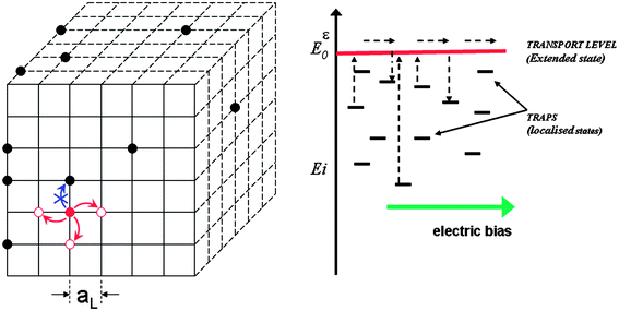 | ||
| Fig. 1 RW numerical simulation on a simple cubic lattice of sites with a multiple-trapping mechanism of transport. Carrier occupying traps are represented by ●. The red circle is the carrier with the minimum waiting time selected to move to a nearest neighbour. Jumps to occupied sites are not allowed. aL is the distance between the traps, which can be related to the total trap concentrations. Waiting times are determined by the difference between the energy of the trap and the energy of the transport level as stated in Eqn (1). | ||
Alternatively, hopping transport can be implemented in a RW simulation31,48,49
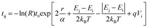 | (2) |
RW simulation based on time is organized as follows. Carriers are given release times according to Eqn (1) or (2) for the energies and positions of the sites they visit. Waiting times are defined as the difference between the release time of the carrier and the time already spent by the carrier in a particular site. For each simulation step the carrier with the shortest waiting time (tmin) is allowed to move. The waiting times for the rest of the carriers are then reduced by tmin and the process is repeated so the simulation advances by time steps of length tmin. This time increment is a variable quantity that depends on the current configuration of the system and the sites occupied at each particular moment. Hence, a RW numerical simulation is an adaptive time-step simulation procedure. The broad dispersion in energies of the sites in nanocomposites, leads to a variation in waiting times of various orders of magnitude, so an adaptive time-step is very convenient to describe transport adequately. In addition, RW simulation is carried out with the restriction that no more than one carrier is allowed per site. As we will see below, this condition is very important to ensure that the model can reproduce basic experimental features like density-dependent diffusion coefficients and conductivities.
The RW method with multiple-trapping transport, particularized for a simple cubic lattice of sites with jumps between nearest neighbours only, was applied by Nelson11 to reproduce dispersive transport in nanocrystalline TiO2. Nelson's simulations were based on the ubiquitous exponential distribution of trap energies14
 | (3) |
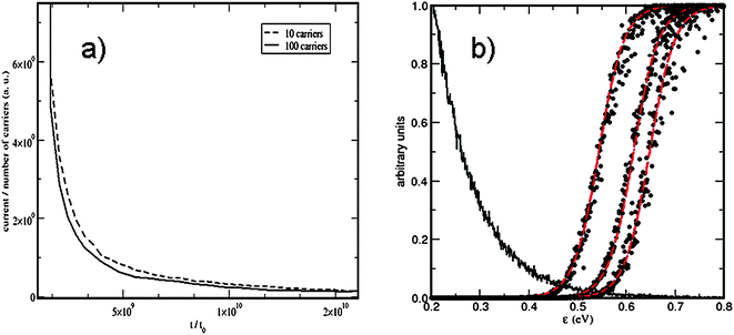 | ||
| Fig. 2 Trap-filling effects in RW simulations. (a) Normalized photocurrent decays in RW simulations in a 40 × 40 × 40 simple cubic lattice with multiple-trapping transport. When the carrier density in the sample is larger the photocurrent decays more quickly (reproduced from Ref. 11). (b) Probability that a trap of energy ε is occuppied in the RW simulation (●). The red lines show the fit to Fermi–Dirac distributions. From left to right the data correspond to calculations with 10 carriers in lattices of 18 × 18 × 18, 24 × 24 × 24 and 28 × 28 × 28 sites (from Ref. 23). | ||
Random walk simulation and dynamics: recombination mechanisms and photovoltage transients
The RW method has been extensively used to understand the molecular mechanism of the back reaction in nanocrystalline solar cells. Recombination losses are important because they determine the open-circuit photovoltage and the overall efficiency of the device. The numerical computation allows one to fit experimental transients and to establish the most likely mechanism of charge recombination. Hence, it has been established16 that the multiple-trapping model can reproduce accurately the charge recombination kinetics in dye-sensitised mesoporous TiO2electrodes. In contrast, the alternative hopping model predicts a different shape of the electron density decays. The good performance of the multiple-trapping RW approach has been also confirmed by experiments and calculations in the presence of an active electrolyte.52,53 The results obtained seem to indicate that the pseudo second order observed in the recombination kinetics is due to trap-limited transport rather than to a true bimolecular mechanism. A different RW application that goes beyond the nearest neighbour approximation18 confirms this conclusion and also, that the energetic disorder is the main factor controlling electron recombination. Despite this, hopping transport can still explain the observed phenomenology if the energy–transport approximation holds for electron transport in nanocrystalline materials.54 The correct transport mechanism also influences the time evolution of the diffusion coefficient and the mobilities.25,55RW simulation shows that the system relaxes in a very peculiar way, in which the whole electron population adopts a “transient” Fermi level that moves steadily towards its equilibrium value.25Recently, the RW method has been applied to model surface photovoltage decays in dye-sensitised nanocrystalline films.28 In this case, experimental data account for the interplay between transport and recombination of electrons with dye molecules. The observed transients reveal anomalous diffusion features. RW simulations can describe the transients over many orders of magnitude. By tuning the characteristic temperature of the trap energy distribution (T0 in Eqn (2)) it is possible to fit the transients accurately (see Fig. 3). Assuming that the true distribution is exponential, the results suggest that the depth of the distribution becomes smaller when the temperature is decreased. The same conclusion has been obtained by other authors.24,56 The crucial influence of the sensitive kinetic balance between charge generation, transport and recombination has been also modelled by RW methods in polymer nanocomposites.34,35
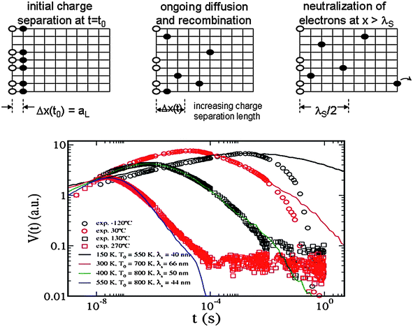 | ||
| Fig. 3 RW simulation of surface photovoltage transients (from Ref. 28). Above: The positive charge (○) is fixed at the surface, whereas the electrons (●) are mobile. The electrons move between neighbouring traps in a simple cubic lattice. Below: experimental photovoltage transients and RW fits. The values of the characteristic temperatures and the screening length λS are shown in the graph. | ||
Towards sophisticated applications: combining energetic and spatial disorder
Although most of the applications of RW simulation have focused on the influence of the energetic disorder on the transport and dynamic properties of disordered materials, interesting work has been done to take into account percolation and morphological effects. Benkstein and coworkers21 carried out RW simulations on ensembles of nanoparticles with fractal geometry. Their model makes it possible to reproduce the reduction of the diffusion coefficient when the porosity of nanocrystalline films is increased. This somehow expected result is attributed to the limitation that the connections between the particles impose on electron transport and can be explained approximately by percolation theory.57 Percolation effects revealed by RW simulation have recently been confirmed experimentally.58The effect of the degree of particle connections, i.e. the coordination number, in combination with electron trapping have been studied thoroughly by Cass and coworkers.20,59 These authors carry out RW simulations with an exponential distribution of traps energies on 3D networks of spheres arranged on an ordered cubic lattice. The results show the key role of connectivity on the charge collection efficiencies in mesoporous electrodes. This work has been extended recently22 to realistic packings of nanoparticles generated from cluster models.60 The new model provides the means to compute the diffusion coefficient, in the presence of electron trapping, for different porosities and nanoparticle sizes (see Fig. 4). The simulated data reproduce the observed porosity dependence and suggest that only if the traps are located on the surface of the nanoparticles is it possible to reproduce the experimental decrease of the diffusion coefficient with grain size.61
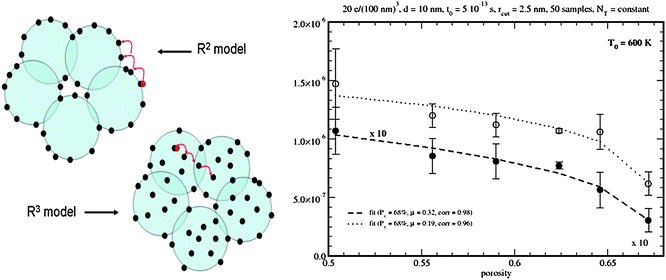 | ||
| Fig. 4 RW models with spatial disorder (from Ref. 22). In the so called R2 model electron traps are located on the surface of the nanoparticles, whereas in the R3 model the traps occupy the whole volume. Results for the diffusion coefficient as a function of the porosity of the film are shown (left). | ||
The effect of geometry and morphology has also been studied in plastic solar cells using RW stochastic techniques.34,35 These studies conclude that there is an optimum size (20 nm) of the domains for which the ratio charge generation/charge separation is maximum. The simulation description opens the way to introduce the combined effect of the mobility ratio and the microscopic geometry32 so that the design and composition of the polymer blend can be optimized for higher efficiencies.62 Recent RW simulations for different geometries and thicknesses36 have shown that nanocrystalline organic solar cells optimize both exciton diffusion and carrier collection, thus providing for highly efficient devices.
Conclusions
RW simulation (also called Monte Carlo) is a potent and versatile technique especially suited to model transport and dynamic processes in solar cells based on disordered and nanostructured materials. The availability of powerful computers in combination with stochastic techniques facilitates the understanding of fundamentals and helps in the design of better performing devices. The possibility of describing the transport process from first principles paves the way for exploring interesting issues such as ascertaining the correct mechanism of transport (hopping or multiple-trapping) or the influence of trap energy distribution. The advent of new architectures such as nanowires and nanotubes and novel devices like those based on quantum dots and extremely thin adsorbers pose challenging problems for the RW technique. Hence, it is interesting to explore how electron diffusion length depends on the morphology of the device, or how the rate and nature of the recombination reactions limit efficiency in solar cell devices.Acknowledgements
The work was supported by Ministerio de Educación y Ciencia of Spain under projects ENE2004–01657/ALT and HOPE CSD2007–00007 (Consolider–Ingenio 2010). JAA also thanks Junta de Andalucía for funding under projects P06–FQM–01869, P07–FQM–02595 and P07–FQM–02600References
- N. Metropolis, A. W. Rosenbluth, M. N. Rosenbluth, A. H. Teller and E. Teller, J. Chem. Phys., 1953, 21, 1087 CrossRef CAS.
- D. Frenkel and B. Smit, Understanding molecular simulation, Academic Press, San Diego, 2002 Search PubMed.
- M. Gratzel, Prog. Photovoltaics, 2006, 14, 429 CAS.
- C. J. Brabec, N. S. Sariciftci and J. C. Hummelen, Adv. Funct. Mater., 2001, 11, 15 CrossRef CAS.
- P. Peumans, S. Uchida and S. R. Forrest, Nature, 2003, 425, 158 CrossRef CAS.
- B. Movaghar, M. Grunewald, B. Ries, H. Bassler and D. Wurtz, Phys. Rev. B, 1986, 33, 5545 CrossRef.
- M. Silver, G. Schoenherr and H. Baessler, Phys. Rev. Lett., 1982, 48, 352 CrossRef.
- H. Bassler, Phys. Status Solidi B, 1993, 175, 15 CrossRef.
- S. D. Baranovskii, A. L. Efros, B. L. Gelmont and B. I. Shklovskii, J. Phys. C: Solid State Phys., 1979, 12, 1023 CrossRef CAS.
- B. I. Shklovskii, H. Fritzsche and S. D. Baranovskii, Phys. Rev. Lett., 1989, 62, 2989 CrossRef CAS.
- J. Nelson, Phys. Rev. B, 1999, 59, 15374 CrossRef CAS.
- H. Scher and E. W. Montroll, Phys. Rev. B, 1975, 12, 2455 CrossRef CAS.
- J. van de Lagemaat and A. J. Frank, J. Phys. Chem. B, 2000, 104, 4292 CrossRef CAS.
- J. Bisquert, F. Fabregat-Santiago, I. Mora-Sero, G. Garcia-Belmonte, E. M. Barea and E. Palomares, Inorg. Chim. Acta, 2008, 361, 684 CrossRef CAS.
- J. Nelson and R. E. Chandler, Coord. Chem. Rev., 2004, 248, 1181 CrossRef CAS.
- J. Nelson, S. A. Haque, D. R. Klug and J. R. Durrant, Phys. Rev. B, 2001, 6320 Search PubMed.
- S. A. Haque, Y. Tachibana, R. L. Willis, J. E. Moser, M. Gratzel, D. R. Klug and J. R. Durrant, J. Phys. Chem. B, 2000, 104, 538 CrossRef CAS.
- A. V. Barzykin and M. Tachiya, J. Phys. Chem. B, 2002, 106, 4356 CrossRef CAS.
- R. L. Willis, C. Olson, B. O'Regan, T. Lutz, J. Nelson and J. R. Durrant, J. Phys. Chem. B, 2002, 106, 7605 CrossRef CAS.
- M. J. Cass, A. B. Walker, D. Martinez and L. M. Peter, J. Phys. Chem. B, 2005, 109, 5100 CrossRef CAS.
- K. D. Benkstein, N. Kopidakis, J. van de Lagemaat and A. J. Frank, J. Phys. Chem. B, 2003, 107, 7759 CrossRef CAS.
- J. A. Anta and V. Morales-Florez, J. Phys. Chem. C, 2008, 112, 10287 CrossRef CAS.
- J. A. Anta, J. Nelson and N. Quirke, Phys. Rev. B, 2002, 65 Search PubMed.
- A. Petrozza, C. Groves and H. J. Snaith, J. Am. Chem. Soc., 2008, 130, 12912 CrossRef CAS.
- J. A. Anta, I. Mora-Sero, T. Dittrich and J. Bisquert, Phys. Chem. Chem. Phys., 2008, 10, 4478 RSC.
- J. van de Lagemaat and A. J. Frank, J. Phys. Chem. B, 2001, 105, 11194 CrossRef CAS.
- J. van de Lagemaat, N. Kopidakis, N. R. Neale and A. J. Frank, Phys. Rev. B, 2005, 71 Search PubMed.
- J. A. Anta, I. Mora-Sero, T. Dittrich and J. Bisquert, J. Phys. Chem. C, 2007, 111, 13997 CrossRef CAS.
- T. Offermans, S. C. J. Meskers and R. A. J. Janssen, J. Chem. Phys., 2003, 119, 10924 CrossRef CAS.
- T. Offermans, S. C. J. Meskers and R. A. J. Janssen, Chem. Phys., 2005, 308, 125 CrossRef CAS.
- J. Nelson, Phys. Rev. B, 2003, 67 Search PubMed.
- C. Groves, R. A. Marsh and N. C. Greenham, J. Chem. Phys., 2008, 129 Search PubMed.
- R. A. Marsh, C. Groves and N. C. Greenham, J. Appl. Phys., 2007, 101 Search PubMed.
- P. K. Watkins, A. B. Walker and G. L. B. Verschoor, Nano Lett., 2005, 5, 1814 CrossRef CAS.
- C. R. McNeill, S. Westenhoff, C. Groves, R. H. Friend and N. C. Greenham, J. Phys. Chem. C, 2007, 111, 19153 CrossRef CAS.
- F. Yang and S. R. Forrest, ACS Nano, 2008, 2, 1022 CrossRef CAS.
- M. Gratzel, Nature, 2003, 421, 586 CrossRef.
- F. W. Schmidlin, Bull. Am. Phys. Soc., 1977, 22, 346 Search PubMed.
- M. Silver and L. Cohen, Phys. Rev. B, 1977, 15, 3276 CrossRef CAS.
- A. Solbrand, A. Henningsson, S. Sodergren, H. Lindstrom, A. Hagfeldt and S. E. Lindquist, J. Phys. Chem. B, 1999, 103, 1078 CrossRef CAS.
- R. Konenkamp, Phys. Rev. B, 2000, 61, 11057 CrossRef CAS.
- L. M. Peter and K. G. U. Wijayantha, Electrochem. Commun., 1999, 1, 576 CrossRef CAS.
- A. J. Frank, N. Kopidakis and J. van de Lagemaat, Coord. Chem. Rev., 2004, 248, 1165 CrossRef CAS.
- J. Bisquert, Phys. Chem. Chem. Phys., 2008, 10, 1 RSC.
- J. Bisquert and V. S. Vikhrenko, J. Phys. Chem. B, 2004, 108, 2313 CrossRef CAS.
- T. Tiedje and A. Rose, Solid State Commun., 1981, 37, 49 CrossRef CAS.
- D. Monroe, Phys. Rev. Lett., 1985, 54, 146 CrossRef CAS.
- A. Miller and E. Abrahams, Phys. Rev., 1960, 120, 745 CrossRef CAS.
- S. D. Baranovskii, H. Cordes, F. Hensel and G. Leising, Phys. Rev. B, 2000, 62, 7934 CrossRef CAS.
- S. V. Novikov, D. H. Dunlap, V. M. Kenkre, P. E. Parris and A. V. Vannikov, Phys. Rev. Lett., 1998, 81, 4472 CrossRef CAS.
- C. Uebing and R. Gomer, J. Chem. Phys., 1991, 95, 7626 CrossRef CAS.
- A. N. M. Green, R. E. Chandler, S. A. Haque, J. Nelson and J. R. Durrant, J. Phys. Chem. B, 2005, 109, 142 CrossRef CAS.
- N. Kopidakis, K. D. Benkstein, J. van de Lagemaat and A. J. Frank, J. Phys. Chem. B, 2003, 107, 11307 CrossRef CAS.
- J. Bisquert, J. Phys. Chem. C, 2007, 111, 17163 CrossRef CAS.
- J. van de Lagemaat, K. Zhu, K. D. Benkstein and A. J. Frank, Inorg. Chim. Acta, 2008, 361, 620 CrossRef CAS.
- I. Abayev, A. Zaban, V. G. Kytin, A. A. Danilin, G. Garcia-Belmonte and J. Bisquert, J. Solid State Electrochem., 2007, 11, 647 CrossRef CAS.
- S. Kirkpatr, Rev. Mod. Phys., 1973, 45, 574 CrossRef.
- A. Ofir, S. Dor, L. Grinis, A. Zaban, T. Dittrich and J. Bisquert, J. Chem. Phys., 2008, 128 Search PubMed.
- M. J. Cass, F. L. Qiu, A. B. Walker, A. C. Fisher and L. M. Peter, J. Phys. Chem. B, 2003, 107, 113 CrossRef CAS.
- V. Morales-Florez, M. Pinero, N. De La Rosa-Fox, L. Esquivias and J. A. Anta, J. Non-Cryst. Solids, 2007 Search PubMed In Press.
- N. Kopidakis, N. R. Neale, K. Zhu, J. van de Lagemaat and A. J. Frank, Appl. Phys. Lett., 2005, 87 Search PubMed.
- C. Muller, T. A. M. Ferenczi, M. Campoy-Quiles, J. M. Frost, D. D. C. Bradley, P. Smith, N. Stingelin-Stutzmann and J. Nelson, Adv. Mater., 2008, 20, 3510 CrossRef CAS.
| This journal is © The Royal Society of Chemistry 2009 |