Copper sulfide as a light absorber in wet-chemical synthesized extremely thin absorber (ETA) solar cells†
Miles
Page‡
,
Olivia
Niitsoo‡
,
Yafit
Itzhaik
,
David
Cahen
* and
Gary
Hodes
*
Department of Materials & Interfaces, Weizmann Institute of Science, Rehovot, 76100, Israel. E-mail: david.cahen@weizmann.ac.il; gary.hodes@weizmann.ac.il; Fax: +972-8934-4137; Tel: +972-8934-2076
First published on 12th November 2008
Abstract
We demonstrate an extremely thin absorber (ETA) solar cell using a copper sulfide (Cu2−xS) light absorber. We compare the cell performance with that of a CdS absorber, to demonstrate the potential and the challenges associated with using low-cost, low-band gap absorber materials to fully exploit the thin-absorber concept.
Broader contextCopper sulfide is in many ways an ideal absorber for solar PV devices, because it combines very good light-absorption characteristics with low cost and non-toxicity, and is one of the few absorber materials (along with silicon) that have sufficient terrestrial abundance to provide a large proportion of future world energy demand. However, its high electron–hole recombination rate makes solar cells based on copper sulfide especially challenging to fabricate.Here we demonstrate a low-energy, low-cost fabrication of an “Extremely Thin Absorber” (ETA) metal oxide (TiO2)–copper sulfide solar cell, using only wet-chemical synthetic techniques (except for the evaporated gold contact). A semiconducting buffer layer between the TiO2 and copper sulfide, and selective application of an insulating surfactant (dodecylphosphonate) monolayer on regions of TiO2 that would otherwise be exposed directly to CuSCN, strongly reduce electron–hole recombination between the electron-conducting TiO2 and hole-conducting CuSCN phases. This interfacial engineering dramatically increases the efficiency of the metal oxide–copper sulfide PV cells, and illustrates a general route to improving ETA solar cells. |
Nanocrystalline thin-film solar cells based on mesoporous metal oxides, especially TiO2 and ZnO, are gaining momentum as potential low-cost photovoltaic cells, due to the availability of their constituent materials and relatively cheap construction process.1,2 One promising concept is the extremely thin absorber (ETA) class of solar cells,2 in which an ultra-thin, light-absorbing semiconductor layer is deposited on the large internal surface of the oxide film, completed with an appropriate pore-filling hole conductor.
The stated goal of the ETA concept is to allow relatively low-quality materials to be employed, due to the short distance through which photogenerated carriers need to be transported before being separated into the respective electron- and hole-conducting phases. Most of the ETA cells up to now have used relatively good quality absorbers (i.e., with relatively low recombination rates), such as CdS,3CdSe,4 PbS5 and In2S3.6
The earliest thin-film solar cells were based on a CdS|Cu2S junction, for which efficiencies of up to ∼10% were reached in the early 1980s.7 Research into these cells was subsequently abandoned due to a combination of factors caused by diffusion of Cu+ ions from the chalcocite (Cu2S) phase into the CdS layer.8,9 The electronic characteristics of copper sulfides (Cu–S) are generally very poor (in particular, fast electron–hole recombination times): the many possible phases, ranging from CuS2 to Cu2S, tend to coexist resulting in a very high propensity for the material to be degenerate, with near-metallic behaviour.
Importantly however, since the non-stoichiometric Cu2−xS (for x < ∼0.2), has similar absorption characteristics to Cu2S (see ESI†), the stoichiometric stability of the Cu–S phase should be less relevant in a copper sulfide ETA cell, if the poor electronic performance is indeed less important.
Copper sulfides can be considered in some ways ideal absorber materials – being non-toxic, cheap and, importantly, abundant, and with good absorption characteristics. Cu2S in particular has a bandgap of 1.2 eV, which is nearly ideal for solar photovoltaic applications. An ETA cell is one of the few configurations with potential to exploit the favourable qualities of Cu–S in a low-cost solar cell. Additionally, Cu–S can be considered a model electronically ‘poor’ semiconductor, and construction of a good solar cell with it would be clear proof of the above-stated ETA principle.
The only reported Cu–S|(flat) MO solar cell, from Cu1.8S|TiO2,10 gave a Jsc of 30 µA cm−2, and Voc of 200 mV at ∼2.8 sun, in spite of favourable theoretical predictions for the similar Cu2S|ZnO combination.11
Here we demonstrate an ETA solar cell using Cu2−xS as an absorber. It is constructed almost exclusively using low-cost materials and low-energy synthetic methods, and gives the best reported performance for a Cu–S|MO solar cell.
The design is illustrated in Fig. 1 (see ESI†for a detailed description). Briefly, a transparent conducting oxide (fluorine-doped tin oxide, FTO) is coated with a dense layer of TiO2,12,13 onto which a mesoporous titania film (P25, Degussa: 25 nm particle size) is applied and sintered.
 | ||
| Fig. 1 SEM image of an ETA cell cross-section, with a schematic illustration of cell components. | ||
CdS is formed on the TiO2 surface by aqueous chemical bath deposition (CBD).14 For Cu2−xS cells, the CdS-coated film is immersed in a hot bath (90 °C) of CuI in 1M aqueous KI, typically for ∼20 s. This results in a solution exchange process converting CdS to Cu2−xS. This exchange process is thought to be topotactic15 and gives a copper sulfide close to Cu2S if Cu2+ ions can be substantially excluded from the Cu+ exchange bath,16 which is achieved in the present system by adding a few drops of hydroxylamine to the CuI–KI bath.
The cell is completed by dipping in aqueous 0.5M LiSCN,3 drying on a hot surface (∼80 °C), and depositing CuSCN from propyl sulfide solution17 by evaporation of the solvent. CuSCN fills pores in the TiO2, and coats the electrode with a layer of CuSCN, preventing shorting of the back contact to the TiO2. Finally a ∼1 cm2gold back contact is added by either electron-beam evaporation or sputtering.
In the case of the Cu2−xS absorber, a buffer layer – a thin layer of material that limits back electron transport, reducing charge carrier recombination – of Inx(OH)ySz,18,19 (In–OH–S), is required for good cell performance. Note that In–OH–S, whether or not treated in the Cu-exchange solution, does not give any appreciable photocurrent, and we therefore discount this buffer layer as a possible source of the photoresponse. The In–OH–S layer is also deposited by CBD on the bare TiO2 surface, followed by CdS and Cu-exchange.
Transmission Electron Microscopy (TEM) characterization of the In–OH–S, CdS and Cu2−xS layers is given in ESI†. By gravimetric analysis, using a specific surface area of 50 m2g−1 for the P25 particles, the CdS|Cu2−xS layer is of 1–2 nm average thickess, and the In–OH–S layer substantially less. Although these values are only a rough guide, as the overall surface coverage of the layers is unknown, they are in agreement with the TEM results. Analysis by energy-dispersive X-ray spectroscopy shows that the sulfides are primarily Cu–S, with much smaller amounts of Cd and In detected. Varying the CdS–Cu2−xS exchange time and temperature, in the case of large (micron-sized) CdS crystals in flat CdS–Cu2S thin film solar cells, resulted in effects on the obtained Cu2−xS phase.16 In the present system however, as might be expected with the very small copper sulfide particles, we observe only a proportionality between reaction time or temperature and the degree of exchange.
The I–V characteristics of Cu2−xS cells, both with and without the In–OH–S buffer layer, and a CdS ‘control’ cell, are shown in Fig. 2. For CdS cells, we obtain lower performance than Larramona et al.,3 with about half the JSC, and a lower VOC (although we have obtained VOC up to 800 mV, but with lower currents). Those authors found their data to be highly dependent on TiO2 particle size, and the best presented data were obtained with particles averaging 50 nm diameter. Solid-state ETA solar cells with the 25 nm particles used herein have not previously been successful.3,20 The reasons for the particle size sensitivity are still not clear, and in our own experiments with larger (∼100 nm) TiO2 particles, no improvement in performance was observed. We suggest that the performance depends sensitively on the degree of percolation in both the TiO2 and CuSCN phases of the bicontinuous network (see below). Careful tuning of the CuSCN deposition process is required to achieve a balance between filling the pores in the TiO2 film with CuSCN, and maintaining the integrity of the TiO2 network: Unfilled pores reduce the effective interfacial area, whereas over-filling appears to result in a mechanical separation of TiO2 domains by growing CuSCN crystals, thus electronically isolating some of the TiO2, and strongly reducing percolation in this phase.
 | ||
| Fig. 2 I–V curves showing the photovoltaic performance of ETA cells with Cu2−xS absorber. Dotted line: no buffer layer; solid line: In–OH–S buffer layer; dashed line: In–OH–S + dodecylphosphonate buffer layers. Inset: An equivalent cell with CdS absorber. | ||
Without a buffer layer, the Cu2−xS absorber under ∼1 sun illumination gives a maximum open circuit voltage (VOC) of 240 mV, with a short circuit current density (JSC) of about 50 µA cm−2 and poor rectification, resulting in fill factors of around 25%. The In–OH–S layer causes a large improvement in the Cu2−xS cell. Though the efficiency (Fig. 2) of 0.06% is still well below that of the CdS absorber (for which we achieve up to 0.4%), it is well in excess of the best reported Cu–S|TiO2 solar cell. Also shown is an equivalent cell in which a dodecylphosphonate monolayer21 is applied to the TiO2 after deposition of the In–OH–S and CdS; and prior to exchange of the CdS to Cu2−xS. This results in a further improvement in JSC at the cost of some voltage, yielding a slightly improved efficiency of 0.07%. This is discussed further below.
While buffer layers improve the performance of DSSCs22 and CIGS thin-film solar cells,23–25 an Al2O3 coating3 on the TiO2 particles in CdS ETA cells has no significant effect. However, CdS has a high bandgap, with a conduction band well above that of TiO2, and thus we suggest that a CdS absorber also acts as a good buffer layer. It can be considered a ‘surface passivating’ material, for which further buffering is not necessarily helpful. Copper sulfide, though, at least on a MO interface, is clearly a ‘surface activating’ (or ‘poor’) absorber material and an effective buffer layer is critical.
It is crucial to stress that our cells were measured through an illumination mask. We found that for both CdS and Cu2−xS-based cells, no assumption of a direct line of current flow could be made, especially for the Cu2−xS cell. When the same (Cu2−xS|In–OH–S) cell as presented in Fig. 2 was measured using a 2 mm diameter contact and no illumination mask, an astonishing 10 mA cm−2 of photocurrent was obtained – more than 20× greater than with a mask. This is an artifact of drawing photocurrent from up to 200 mm2 (the approximate total cell size) surrounding the contact. The final current density of 0.4 mA cm−2 was obtained from a 30 mm2 contact, with illumination through an equal-sized mask. A range of Jsc ∼0.1–0.4 mA cm−2, and VOC ∼300–400 mV was typically found for these cells. This value increases to 0.4–0.6 mA cm−2 with the addition of the alkylphosphonate layer, with a VOC of ∼300 mV.
The incident wavelength-dependent photocurrent (Fig. 3), for several different cell designs, serves to demonstrate the potential for improvement of the Cu2−xS cell. The presented results were calculated from the raw photocurrent data using a calibrated, commercial photodiode as a reference. In Fig. 3(a), they have also been scaled to the saddle in the photoresponse (at ∼405 nm) between the TiO2 peak (∼370 nm) and the onset of the visible light response. Scaling is necessary for the direct comparison of these cells of varying overall performance. External quantum efficiencies, measured in the presence of background white light,14,26 are shown in Fig. 3(b) for two cells. The peak quantum efficiencies were 16.1% for the CdS cell, and 5.7% for the Cu2−xS/phosphonate cell. These values are underestimated; due to slow electron diffusion in the TiO2, very low chopper frequencies (<1 Hz, not attainable in our setup) are necessary to determine absolute quantum efficiency as has been previously shown for DSSCs.26
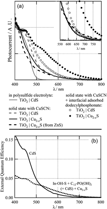 | ||
| Fig. 3 (a) Relative photocurrent as a function of wavelength of CdS cell in polysulfide electrolyte.14 The plots are scaled to allow comparison between cells of varying performance (see text). Inset: Zoomed view of photocurrent over the 550–800 nm range. (b) External quantum efficiency of a solid-state CdS cell (solid line) and Cu2−xS cell with In–OH–S and dodecylphoshonate buffer layers (dotted line). | ||
A reference curve (Fig. 3(a), solid grey line) is given from an identical TiO2|CdS electrode, coupled with a polysulfide electrolyte to form a photoelectrochemical cell14 with no copper present, giving a photoresponse up to around 500 nm. The equivalent solid-state cell (dashed grey line), shows a significant tailing effect, out to ∼700 nm. This can also be identified in ref. 2, and we attribute this to a Cd–Cu exchange process occurring during deposition of the CuSCN, leaving a small amount of Cu–S in the absorber layer. Because of this Cu–S already present in the solid-state CdS cell, the photoresponse range of the regular Cu2−xS cell (solid black line) is not appreciably affected (Fig. 3, inset).
A Cu2−xS cell was also made from a CBD ZnS film, (including an In–OH–S layer), and Cu-exchanged as for the CdS-based cell. Unlike CdS, ZnS does not absorb visible light and cannot be responsible for the photoresponse. Its spectral response (dashed black line) is very similar, particularly in the long wavelength region, to that of a CdS-based cell, confirming that Cu2−xS is the primary absorber in these cells. The alternative possibility, that the response arises from Cu-doped ZnS, would require the unlikely coincidence that it gives a near-identical spectral response to either Cu2−xS or Cu-doped CdS. We do not rule out the possibility of a contribution from unexchanged CdS.
The spectral response of both these cells is still poor compared with their visible absorption spectra (see ESI†). However, the additional buffer layer of alkylphosphonate (dotted line; see also Fig. 2, dashed line) gives a very strong improvement in the red response, out to 800 nm with a much broader quantum efficiency peak. It also gives a substantial, although lesser, improvement in the CdS cell, open circles in Fig. 3(a). This is expected in view of our assumption that some Cu–S is already present after CuSCN deposition onto CdS.
The effect of the alkylphosphonate is presumably the result of passivation of the TiO2 surface by the monolayer. Dark I–V measurements (ESI†) show a decrease in current passed in both bias directions for alkylphosphonate-treated films, independent of which of the various absorber and buffer layers are present (ESI†). The passivation appears to lead to a longer electron diffusion length in the TiO2 phase – the absolute quantum efficiencies at long wavelengths are greater than those of cells without the molecular layer, as shown in Fig. 3(b). This allows current collection further from the FTO substrate, where longer wavelength absorption is favoured. In the solar spectrum, these longer wavelengths (500![[thin space (1/6-em)]](https://www.rsc.org/images/entities/char_2009.gif) –∼1000 nm) are more intense than the shorter wavelengths, but with TiO2 being the limiting charge transport phase,27 the resulting electrons are more likely to be lost to recombination in the absence of the molecular layer.
–∼1000 nm) are more intense than the shorter wavelengths, but with TiO2 being the limiting charge transport phase,27 the resulting electrons are more likely to be lost to recombination in the absence of the molecular layer.
Such a passivation effect should normally result also in an increase in the VOC of the cell, in the absence of other effects, contrary to our results (Fig. 2). Contact Potential Difference measurements on the TiO2 film showed that the alkylphosphonate layer decreased the work function of the system by 0.2 eV in the dark, and by 0.3 eV under illumination from a tungsten halogen lamp. This could explain the loss in VOC if, for example, the Fermi level of the TiO2 has been raised relative to the conduction band after adsorption of the electron-rich phosphonate group. The origin of effects imparted by the molecular layer is currently under further investigation.
To summarize, despite the thin layer configuration, the electronic quality of the absorber clearly cannot be neglected. However, already these first results indicate that an electronically poor semiconductor such as Cu2−xS may be able to give a good quality ETA solar cell. The increased performance from a simple In–OH–S buffer layer suggests that a larger improvement is possible. The critical challenge is effective surface passivation; some care to optimize the In–OH–S layer was taken, but full coverage of the mesoscopically rough surface is unlikely, and a large contribution to charge recombination in this buffered cell probably arises from intermittent TiO2–Cu2−xS contact. This was reduced by adding the molecular dodecylphosphonate layer, further increasing the photocurrent.
Both the choice of buffer layer, and achieving conformal coverage of the interface, are obvious routes to improving performance. Molecular monolayers have been investigated also in DSSCs, to control interfacial energy level alignment.28 We are pursuing the use of these monolayers in ETA cells further.
Effective percolation in both phases probably remains another primary loss mechanism, at least in very small (<30 nm) particle cells. Combining percolation and buffering into a cheap solar cell construction remains a significant technological challenge which nevertheless, if it can be overcome, will allow a very large library of potential absorber materials to be exploited in low-cost metal oxide-based solar cells.
Acknowledgements
This work was supported by the Israel Ministry of Science, Culture and Sport and by the International Copper Association + Center for Advanced Interdisciplinary Research in Materials (ICA/CIMAT). DC thanks 21 Ventures and Jack Halpern for research grants. DC and ON thank the Nancy and Stephen Grand Center for Sensors and Security and the NATO Science for Peace program for partial support. We acknowledge the Harold Perlman family's historic generosity. We are also happy to acknowledge Hal Emmer, Alexander D. Kraus and Christopher A. Zimmerman for experimental assistance and Jacques Vedel and Michael Kokotov for invaluable discussions.References
- L. M. Peter, Phys. Chem. Chem. Phys., 2007, 9, 2630 RSC.
- C. Levy-Clement in Nanostructured materials for solar energy conversion, Elsevier 2006, ed. T. Soga, ch. 14, p. 447 Search PubMed.
- G. Larramona, C. Chone, A. Jacob, D. Sakakura, B. Delatouche, D. Pere, X. Cieren, M. Nagino and R. Bayon, Chem. Mater., 2006, 18, 1688 CrossRef CAS.
- C. Levy-Clement, R. Tena-Zaera, M. A. Ryan, A. Katty and G. Hodes, Adv. Mater., 2005, 17, 1512 CrossRef CAS.
- R. Bayon, R. Musembi, A. Belaidi, M. Bär, T. Guminskaya, M.-C. Lux-Steiner and T. Dittrich, Sol. Energy Mater. Sol. Cells, 2005, 89, 13 CrossRef CAS.
- D. Kieven, T. Dittrich, A. Belaidi, J. Tornow, K. Schwarzburg, N. Allsop and M. Lux-Steiner, Appl. Phys. Lett., 2008, 92, 153107 CrossRef.
- J. A. Bragangolo, A. M. Barnett, J. E. Phillips, R. B. Hall, A. Rothwarf and J. D. Meakin, IEEE Trans. Electron Devices, 1980, 27, 645 CrossRef.
- K. Moitra and S. Deb, Sol. Cells, 1983, 9, 215 CrossRef CAS.
- L. H. Allen and E. Buhks, J. Appl. Phys., 1986, 59, 1360 CrossRef CAS.
- L. Reijnen, B. Meester, A. Goossens and J. Schoonman, Mater. Sci. Eng., C, 2002, 19, 311 CrossRef.
- M. Burgelman and H. J. Pauwels, Electron. Lett., 1981, 17, 224 CrossRef CAS.
- Y. Ohya, H. Saiki, T. Tanaka and Y. Takahashi, J. Am. Ceram. Soc., 1996, 79, 825 CrossRef CAS.
- Y. Takahashi and Y. Matsuoka, J. Mater. Sci., 1988, 23, 2259 CAS.
- O. Niitsoo, S. K. Sarkar, C. Pejoux, S. Rühle, D. Cahen and G. Hodes, J. Photochem. Photobiol., A, 2006, 181, 306 CrossRef CAS.
- F. Pfisterer, Thin Solid Films, 2003, 431–432, 470 CrossRef CAS.
- A. Stanley, Appl. Solid State Sci., 1975, 5, 251 Search PubMed.
- B. O'Regan, F. Lenzmann, R. Muis and J. Wienke, Chem. Mater., 2002, 14, 5023 CrossRef CAS.
- D. Braunger, D. Hariskos, T. Walter and H. W. Schock, Sol. Energy Mater. Sol. Cells, 1996, 40, 97 CrossRef CAS.
- R. Bayon, C. Guillen, M. A. Martinez, M. T. Gutierrez and J. Herrero, J. Electrochem. Soc., 1998, 145, 2775 CrossRef CAS.
- R. O'Hayre, M. Nanu, J. Schoonman and A. Goossens, Nanotechnology, 2007, 18 Search PubMed 055702.
- G. Nesher, H. Shpaisman and D. Cahen, J. Am. Chem. Soc., 2007, 129, 734 CrossRef CAS.
- E. Palomares, J. N. Clifford, S. A. Haque, T. Lutz and J. R. Durrant, J. Am. Chem. Soc., 2002, 125, 475.
- F. Lenzmann, M. Nanu, O. Kijatkina and A. Belaidi, Thin Solid Films, 2004, 451, 639 CrossRef.
- D. Hariskos, S. Spiering and M. Powalla, Thin Solid Films, 2005, 480–481, 99 CrossRef CAS.
- S. Siebentritt, Sol. Energy, 2004, 77, 767 CrossRef CAS.
- J. Hohl-Ebinger, A. Hinsch, R. Sastrawan, W. Warta and U. Würfel, 19th EUPVSEC (Paris, France, June 11–19), 2004, 173 Search PubMed.
- B. O'Regan and F. Lenzmann, J. Phys. Chem. B, 2004, 108, 4342 CrossRef CAS.
- S. Rühle, M. Greenshtein, S. G. Chen, A. Merson, H. Pizem, C. S. Sukenik, D. Cahen and A. Zaban, J. Phys. Chem. B, 2005, 109, 18907 CrossRef.
Footnotes |
| † Electronic supplementary information (ESI) available: Experimental, TEM characterization, copper sulfide phases, optical spectra and passivation. See DOI: 10.1039/b813740d |
| ‡ These authors contributed equally to the research. |
| This journal is © The Royal Society of Chemistry 2009 |