Impedance spectroscopy characterisation of highly efficient silicon solar cells under different light illumination intensities
Iván
Mora-Seró
a,
Germà
Garcia-Belmonte
a,
Pablo P.
Boix
a,
Miguel A.
Vázquez
b and
Juan
Bisquert
*a
aPhotovoltaics and Optoelectronic Devices Group, Departament de Física, Universitat Jaume I, 12071, Castelló, Spain. E-mail: bisquert@fca.uji.es
bIsofoton, S.A. Avda. Severo Ochoa, 50, 29590, Málaga, Spain
First published on 17th March 2009
Abstract
Highly efficient silicon solar cells have been characterised by impedance spectroscopy and current–potential characteristic in the dark and with different illumination intensities. For each illumination the impedance behaviour has been analysed at different applied bias potentials, in the forward and reverse region, comparing the results with the current–potential characteristic. Different cell parameters, as series and parallel resistances, capacitance, diode factor, minority carrier lifetime, acceptor impurities density and depletion layer charge density have been obtained as a function of bias voltage for different light illumination intensities. The effect of light-generated carriers and applied bias in the behaviour of the solar cell under illumination is discussed.
Broader contextDetermining the characteristics of the performance of solar cells is essential to improve their optimization for sunlight energy conversion. Impedance spectroscopy is a valuable tool in many areas of materials science and devices and is applied here to several highly efficient commercial monocrystalline silicon solar cells. We provide a perspective of the connection between models for different classes of solar cells. The analysis of experimental results shows that in Si solar cells it is possible to separate the physical components of the capacitance, as well as to monitor the variation of the different internal resistances over different conditions of bias voltage and illumination. |
1. Introduction
The impedance spectroscopy technique consists of the frequency analysis of ac behaviour and is widely applied in a broad class of materials systems and devices, including inorganic, organic and biological systems. In solar cell science and technology the most commonly applied frequency technique is admittance spectroscopy. It should be remarked that impedance and admittance are reciprocal functions, so that they give exactly the same information. However, by tradition admittance spectroscopy denominates a special method that operates at reverse voltage and evaluates the energy levels of the majority of carrier traps (in general, all those that cross the Fermi level) as well as trap densities of states.1 In contrast to this, in electrochemistry one is usually more interested in injecting electronic charge into the electrode, and the term generally adopted is impedance spectroscopy. In solar cells it is clearly important to perform frequency analysis in the reverse region of the diode characteristics, since this probes the selectivity of the contacts. However even more critical is to determine the mechanisms governing the photovoltaic performance between short-circuit and open-circuit conditions, which is the operation range for extracting energy (Fig. 1). In this range we probe a variety of situations, from strong carrier accumulation at open circuit, towards rapid extraction at short-circuits. In these conditions, we prefer to denominate the voltage-to-current frequency domain analysis impedance spectroscopy (IS).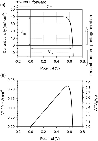 | ||
| Fig. 1 (a) Theoretical calculation of the current density–voltage characteristic of a solar cell (ideal diode model) with Jsc = 40 mA cm−2, and Voc = 0.65 V. Also indicated are the different regions of the applied bias voltage and of the dominant current. (b) The power output of the solar cell. The left vertical axis is normalized to the incident power of 1 sun and gives the conversion efficiency, and the right axis normalization gives the fill factor (FF = 0.84 at maximum power). | ||
By exploring the forward bias range, both in dark and under illumination with different light intensities, a variety of properties can be separately investigated, including transport in the photoactive layer, contacts, bulk and surface capacitance, etc. This approach has been amply used in recent years for dye-sensitized solar cells (DSC)2–8 and organic solar cells,9,10 while there are only a few works to date on solid state devices, such as those based on nanocrystalline/amorphous Si,11–13 thin-film CdTe/CdS,14 GaAs/Ge15,16 and CdS/Cu(In,Ga)Se2 solar cells.17
In this work we present the result of IS characterization of highly efficient silicon solar cells in both forward and reverse bias in dark and under different light intensities. We apply the methods and models that have been extensively used in recent years in the DSC area.2,8 The motivation of this work is twofold. Monocrystalline Si cells stand as a reference in the market and in performance, therefore we believe it is quite useful to describe the IS properties of such solar cells, so that results of IS on new concepts of solar cells can be compared to these. The Si layer is homogeneous so there is a unique medium without complications of grain boundaries, multiple phases, etc., and in addition the selective contacts at the junctions have been optimized for optimal electrical (as well as optical) performance. Thus we expect to obtain IS responses close to ideal theoretical solar cell models.18,19
In addition IS is a very promising method for improving the performance of already very efficient solar cells helping to detect the origin of limitations to energy conversion and stability, and some of these applications have been shown in a number of instances in Si solar cells by our group.12,13 Therefore it is also practical to provide a general outline of the highly efficient Si solar cell impedance response over a broad range of conditions so that specific technical work can be later based on the general characteristics described here.
2. Experimental
The solar cells used in this study are the BP “Saturn” solar cell manufactured by BP Solar in Spain,20 based on the laser-grooved buried grid (LGBP) cell concept, and Isofoton monocrystalline silicon solar cell. The Isofoton cell structure is npp+ and it is built from p-type monocrystalline silicon wafer by aluminium BSF and POCl3 diffusion, the electrical contacts are made by screen-printing technology.The BP solar cell is made of p-silicon wafer (typical minority carrier lifetime is 25 µs21) and incorporates several optical engineering elements such as random textured surface to reduce reflectance, and a back surface field to reduce recombination. Buried in the laser-carved grooves of LGBP cells are narrow deep metal fingers, made of silver-covered electroless copper, which provide excellent electrical conductivity with minimised ohmic losses and low light obscuration. From the original solar cells from BP (156 cm2) and Isofoton (95 cm2) smaller pieces of 0.49 cm2 and 1.20 cm2 were cut following its crystalline cleavage planes, in order to obtain a homogeneous illumination in all the cell surface. The cut cells will be denoted as small cells in the discussion part. Characteristic photovoltaic parameters for the BP solar cells are:21 Short-circuit current Jsc = 37 mA cm−2, open-circuit voltage Voc = 0.66 V, fill factor FF = 0.81, and power conversion efficiency at 1 sun illumination intensity Eff = 20.0%.
The structure of the Isofoton solar cell, made from boron doped p-type Cz–Si, is shown in Fig. 2. The substrate has been textured in alkaline solution to reduce the surface damage from the wire-sawing process and to decrease the reflectivity, after that the phosphorous diffusion process is carried out to manufacture the p–n diode. A silicon nitride layer is used as an antireflective coating to reduce the reflectivity and to passivate the frontal surface and the volume wafer. Electrical contacts to extract the electrical current are made by screen-printing technology. These solar cells come from production line and their characteristic electrical parameters are the following: Jsc = 36 mA cm−2, Voc = 621 mV, FF = 78.4% and Eff = 17.4%.
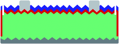 | ||
| Fig. 2 Scheme of ISOFOTON Si solar cell. The green area is the p-type silicon substrate, the red area represent the phosphorus diffused n-type silicon, the blue one is the antireflective coating and the grey areas are the metal contacts. | ||
Impedance measurements and current–potential curves were made with an Autolab PGSTAT-30 equipped with a frequency analyzer module. These measurements were carried out in the dark and under different illumination intensities employing a halogen lamp. No system to control the cell temperature under illumination was used, as a consequence lower values for Voc than the nominal ones have been measured due to the heating by the illumination system. Bias potentials ranged between 0.6 and −0.6 V while 10 mV ac perturbation was applied in impedance measurements ranging between 1 MHz and 1 Hz. All the experiments have been achieved inside a Faraday's box. The contribution of the setup to the measured impedance spectra has been measured short-circuiting the measurement system obtaining a setup resistance of Rsetup = 0.46 Ω. Additionally the connecting wires also introduce an inductive behavior at high frequencies. These contributions have been taken into account in order to obtain the correct cell parameters.
3. Theory of steady-state and impedance behaviour
It is well established that the main processes governing carrier extraction in solid state crystalline solar cells are minority carrier diffusion and recombination.22,23 Schematic energy diagrams of the silicon solar cell are provided in Fig. 3. The diagrams qualitatively illustrate the main concepts and are not drawn to scale, in particular the depletion layer is exaggerated, see below. Note that the space–charge layer in the p semiconductor, characterized by the potential Vsc (defined positive), decreases width w at increasing forward bias. The bias potential in the solar cell can be written| V = Vs + VF | (1) |
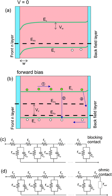 | ||
| Fig. 3 (a) and (b) show energy schemes of the p-doped semiconductor with electron-extracting contact (front p–n junction) at the left and electron blocking contact (back p+ region) at the right. Ec is the edge of the conduction band, Ev is the edge of the valence band, EFn is the electron Fermi level and EFp = EF0 is the whole Fermi level. Vbi is the built-in potential, VF is the potential associated to separation of the Fermi levels, and w the size of the depletion region at the front side. In (b) are shown the processes of (1) electron transport and (2) bulk and (3) back surface recombination. Below are shown the transmission line representation of the diffusion–recombination impedance, being rtr the distributed transport resistance, rrec the bulk recombination resistance, and cµ the chemical capacitance, two cases, (c) corresponds to the blocking (reflecting) boundary condition at the back layer, and (d) with the surface recombination resistance rs, that gives an ohmic contact boundary condition for rs → 0. | ||
Here Vs is the potential in the series resistance and
| VF = Vsc − Vbi | (2) |
| EFn − EF0 = qVF | (3) |
 | (4) |
In this last equation we used the Boltzmann statistics
| n = Nce−(Ec − EFn)/kBT | (5) |
 | (6) |
When the cell is reverse biased, the electron Fermi level becomes low, Fig. 3(a), and the space–charge region increases. The thickness of the depletion layer relates to the voltage as
| w = w0Vsc1/2 | (7) |
 | (8) |
 | (9) |
 | (10) |
Hence Cdl−2 depends linearly on Vsc. Eqn (10) is valid insofar as the space charge region is much larger than the Debye length.
In IS analysis of solar cells, the interpretation of the capacitance is essential as a primary step to determine the right model that describes carrier transport and recombination. Associated with the model of Fig. 3 is the observation of the Mott–Schottky (MS) characteristic in the homogeneous semiconductor, eqn (10), that indicates clearly the presence of excess majority carrier of one kind. In addition, the observation of the chemical capacitance directly indicates accumulation of minorities by the displacement of the Fermi level with respect to the respective band edge, Fig. 3(b). In these conditions it is most likely that extraction of photogenerated minority carriers occurs by diffusion, in addition to a drift component from the space–charge region, where the electrical field is large. Then the major considerations that must be established are: (1) the size of the depletion region and (2) the size of the diffusion length, both with respect to bulk semiconductor size, L.
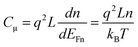
Fig. 4(a) illustrates the dependence on potential (VF) of the total capacitance that should be measured,12 and its components, the chemical capacitance, and the depletion layer capacitance, according to the model expressions outlined above. Parameter values are similar to those obtained in the experimental results, see below. An important point is the exponential dependence of the chemical capacitance, which makes Cµ dominate the total capacitance at sufficient forward bias. We note also the temperature dependence (via equilibrium statistics of carrier occupation in band levels) of Cµ, which delays the prevalence of Cµ to higher bias at higher temperatures. Fig. 4(c) displays the MS linear plot of the capacitance of the space charge region, and Fig. 4(b) shows that the width of the depletion layer is insignificant with respect to the bulk semiconductor size, which is about L = 200 µm. This highlights the fact that photon collection in the space–charge region can be totally neglected with respect to that in the neutral region.
 | ||
| Fig. 4 Theoretical calculation of: (a) capacitances in the solar cell: chemical capacitance Cµ (calculated at two different temperatures, as indicated), capacitance in the depletion layer Cdl, and total capacitance (thick line). (b) Width of the space charge region. (c) Mott–Schottky plot. Parameters used in the simulation: L = 300 µm, T = 300 K, Vbi = 0.65 V, εr = 1, NA = 1016 cm−3, n0 = 1 × 108 cm−3. | ||
The diffusion length, is obtained from electron diffusion coefficient, Dn, and electron lifetime, τn, as  , and indicates the average distance that generated or injected electrons travel before recombining. Influence of Ln in the carrier distribution is illustrated in Fig. 5, for a solar cell in forward bias in dark conditions. For long diffusion length and reflecting boundary (1), the carrier profile is nearly homogeneous. For short diffusion length (2), a gradient of carriers of the size of the diffusion length is built from the injection point. Another crucial factor is the rate of recombination at the back surface. If the rate is large (3), excess carriers cannot be maintained at this boundary, and a gradient of the size of the semiconductor layer is built.
 | ||
| Fig. 5 Concentration in diffusion-recombination model for electrons injected at the left boundary with concentration ns in excess of equilibrium concentration n0. Curve (1) represents the case Ln ≫ L, where Ln is the diffusion length and L the thickness of the layer, for reflecting boundary condition at the back contact. Curve (2) is the case of a short diffusion length, Ln << L, as indicated. Curve 3 corresponds to long diffusion length with strong recombination at the back contact. | ||
An estimation of the diffusion length from the values of electron diffusion coefficient, Dn = 36 cm2 s−1, crystalline silicon typical electron lifetime τn = 2.5 ms gives Ln = 0.3 cm.22 Instead, electron lifetime of τn = 25 µs, caused by surface recombination in p-silicon solar cells, reduces the diffusion length to Ln = 300 µm. This means that gradients of electron distribution should be very low, because the diffusion length results of the order of absorber thickness. Therefore, in a first approximation, the p-Si solar cell operates by accumulating carriers homogeneously in the crystalline semiconductor layer, that are separately extracted by the selective contacts at both sides.18 As a contrasting case, we may mention amorphous silicon solar cells with a pin structure and a very low carrier mobility.26 In this case Ln is very short, and thus the extraction of carriers requires, besides the n and p layers that function as selective contacts, a strong space charge region, formed by accumulation of the slow carrier.
Having summarized the main models of capacitance and steady-state behaviour of homogeneous inorganic semiconductor solar cells, let us discuss the general characteristics of such models in IS technique.
We consider first the properties of the impedance associated with diffusion coupled with recombination. The impedance model has been amply described previously.2,27 The model may be represented as a distributed equivalent circuit, a transmission line shown in Fig 3(c) and (d). Note that the series resistance has not been included in this representation, and it will be added later on. It should be mentioned that a series resistance does not change the spectral features in IS, since it only causes a horizontal displacement of the spectra in the complex plane representation.
The model corresponding to the reflecting boundary condition is shown in Fig. 3(c) and contains three main elements. The first is the chemical capacitance Cµ already discussed above. The second is the recombination resistance
 | (11) |
| Rtr = Lσn−1 | (12) |
Using the Einstein relation,28 the conductivity relates to the free electrons diffusion coefficient as
| σn = CµDn/L | (13) |
It is important to remark the following property2
 | (14) |
Therefore for a long diffusion length it is obtained that Rrec ≫ Rtr. Thus the transport resistance rtr in the upper transport channel looses relevance with respect to the recombination resistance, and the transmission line is reduced to the equivalent circuit shown in Fig. 6(a). The complex plane representation of the impedance model in Fig. 3(c) is shown in Fig. 7(a). It features a major arc that corresponds to the parallel combination of Rrec and Cµ, Fig. 6(a). Note that by eqn (11) the frequency at the top of the arc corresponds to minority carrier lifetime, which can be thus very readily determined by IS. The validity of this technique was confirmed in comparison with quasi-steady-state photoconductance measurements.13
 | ||
| Fig. 6 The ac equivalent circuits for a solar cell. (a) Reduced circuit from the general transmission line of Fig. 2(c) in the case rtr << rrec. (b) The reduced circuit with additional elements: series resistance, back surface recombination resistance, and depletion layer capacitance. (c) Basic circuit for fitting experimental data of the silicon solar cell. | ||
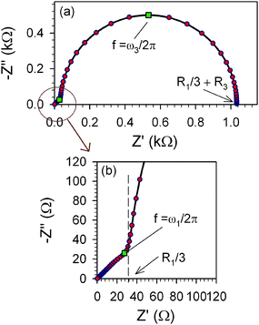 | ||
| Fig. 7 Simulation of the diffusion–recombination impedance with reflecting boundary condition at the back contact and Ln = 3.1L. Parameters Rtr = 1 × 10² Ω cm−2, Rrec = 1 × 10³ Ω cm−2, Cµ = 5 × 10⁻⁶F cm−2. Shown are the characteristic frequency of the low frequency arc (square point), related to the angular frequency ωn = τn−1 = 1/RrecCµ, where τn is the carrier lifetime; the low frequency resistance; and the characteristic frequency of the turnover from Warburg behaviour to low frequency recombination arc (square point), related to the angular frequency ωtr = Dn/L2 = 1/RtrCµ, where Dn is the minority carrier diffusion coefficient. | ||
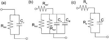
From the point of view of the individual solar cell performance at steady state, the capacitances in the equivalent circuit vanish, and the crucial components are the resistances. It should also be mentioned that in the ac equivalent circuit of Fig. 6(a), the (bias dependent) resistance Rrec, represents the diode behaviour in dc conditions.19 Additional important components of the solar cell equivalent circuit are shown in Fig. 6(b), including a series resistance (usually associated to contacts) and the depletion layer capacitance. Cµ and Cdl are connected in parallel, since both are governed by the same potential, VF, see Fig. 3(a) and (b). Taking into account the combinations in the equivalent circuit of Fig. 6(b), we arrive at that in Fig. 6(c) for the analysis of experimental data.
We have already described above the general properties of the capacitance, which increases at forward bias potential, Fig. 4. From a technical perspective, the capacitance is also significant in some respects. When several panels are connected the increased capacitance has considerable effect on the design of the switching regulators used to control the voltage of the solar panels. Usually, measurement of C-V characteristics does not take into account the series resistance and can provide an erroneous potential dependence of the capacitance, specially at high forward bias where the potential drop at the series resistance could be important due to the high electric current. In this respect, IS is an excellent technique to achieve the capacitance characterization because it can discriminate between series and parallel resistances, at the same time that the capacitance is measured, as it is indicated in Fig. 6(c).
So far, we have neglected the influence of diffusion in the impedance response of Fig. 6. But in addition to the semicircle feature, when Ln ≈ L, the transport resistance plays an important role in the impedance. As shown in Fig. 7(b), diffusion gives a 45° feature in the high frequency part of the complex plot (often called a “Warburg” part, although strictly speaking this term denominates the semi-infinite diffusion impedance). The size of the semicircle is Rrec but that of the Warburg part is Rtr/3. For example taking Ln = 300 µm in a L = 200 µm cell, we expect Rtr = 0.44 Rrec, so the contribution of the Warburg part resistance is 0.15 Rrec, and this should be clearly observable in the impedance spectra. In contrast with the same Ln, for a short solar cellL = 10 µm, the contribution of diffusion in the impedance, Rtr = 1 × 10⁻³Rrec, becomes a very minor feature. In dye-sensitized solar cells, the diffusion length is of the order of the thickness of the diffusion layer, 10 µm, and the Warburg part is routinely measured.8 Another reason for not observing the transport resistance is the presence of other features at high frequency that overlap the Warburg part, as inductive behaviour at high frequency due to the connecting wires, or the observation of the chemical capacitance of the majority carrier (holes).12
Another very important feature, from the technical point of view, is the recombination rate at the back surface. It is widely admitted that the dominating loss mechanism in heterojunction thin-film solar cells is the Shockley–Read–Hall (SRH) recombination at states on the device interfaces.29 In the solar cells of the present study the back contact is formed of a p+ layer that blocks electrons. Such a layer for reducing surface recombination (and in addition, for improved optical reflection) is the most critical step in the preparation of high efficiency industrial cell.30 In IS this feature is represented by the surface recombination resistance Rsur. Since surface recombination is a boundary condition, Rsur appears as a final resistance in the transmission line, as shown in Fig. 3(d). These more general boundary conditions for diffusion impedance have been analysed previously.31,32 However, Fig. 3(d) should be considered a simplification of the circuit models corresponding to SRH recombination in steady-state conditions that were proposed some decades ago by Chan and Sah,33 with a high degree of generality.
In the simplified circuit for fast diffusion, Fig. 6(b), we obtain that bulk and surface recombination resistances are connected in parallel, and could not be distinguished by spectral features. However, the presence of surface recombination requires a very careful analysis of the impedance spectra. First, it was shown in heterojunction solar cells with thin a-Si:H films deposited on c-Si wafers, that description of the surface recombination requires the use of separate components for both electrons and holes chemical capacitance and recombination resistance.12 Second, if transport resistance is observed, the surface recombination resistance introduces a strong modification of the spectra of Fig. 7.32
4. Results and discussion
Very similar results have been obtained for both BP and Isofoton solar cells. Classical current–potential analysis at different light intensities, Fig. 8, reflects a good performance of the small BP cell studied with high efficiency of 12% under 1 sun illumination conditions (Jsc = 35 mA cm−2, Voc = 0.48 V, FF = 0.7). The reduction of efficiency compared to the nominal values are due to the decreased Voc with the increase of temperature and to the reduction of the FF as a consequence of the increase of the series resistance in the small cell, see below for a further discussion of this point. A set of the impedance spectra obtained for different illumination intensities for both forward and reverse bias voltage in the BP small cell are plotted in Fig. 9(a) and (b), respectively. The impedance pattern observed in all the cases consist basically in a semicircle. It can be described by means of the simple equivalent circuit shown in Fig. 6(c), where Rs is a series resistance and Rp is a parallel resistance that should be identified with the recombination resistance Rrec (i.e., this Rp already represents the diode characteristic and not a separate “shunt” resistance). It has been checked experimentally that these resistances scale linearly with the inverse of the cell area, consequently higher values are obtained for the small cells. C in Fig. 6(c) represents the parallel association of the chemical capacitance, Cµ,24 and the depletion-layer capacitance, Cdl, due to space–charge region. As discussed above, Fig. 4, these capacitances depend on bias voltage; Cdl dominates at reverse bias, while at forward bias the chemical capacitance must finally dominate when the concentration of minorities is large. For higher forward potentials an inductive behaviour is observed at the high frequency range (not shown in Fig. 9), and a series inductance, due to the connecting wires, must be added in the equivalent circuit of Fig. 6(c) to fit the whole impedance spectra. This inductance has no meaning for the solar cell operation but the use of such elements in the equivalent circuit improves the determination of the physical parameters. Additionally at high forward bias, the observed semicircle for small cells is distorted at high frequencies and a combination of two semicircles is observed, see Fig. 9(a). For the complete cell this additional arc is not observed (not shown). The origin of this additional arc is the chemical capacitance of holes.12 The Rrec associated with this arc is significantly smaller than the recombination resistance associated with the electrons (arc at lower frequencies), but as this resistance also scales with the inverse of the area for cells with large area, its value is lower than the Rsetup and it could not be discriminated. In the aim of clarity and because it does not affect complete cells, we are not going to further consider this arc in the discussion. We refer to a previous study for a description of this additional effect.12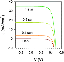 | ||
| Fig. 8 Experimental current density–voltage characteristics measured under different light intensities (small BP solar cell). | ||
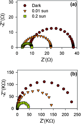 | ||
| Fig. 9 Impedance spectra for three different illumination intensities. (a) Forward bias V = −0.2 V; (b) Reverse bias V = 0.5 V (small BP solar cell). | ||
The impedance pattern corresponding to our solar cells should be similar to that of Fig. 7(a) derived from the equivalent transmission line for blocking conditions of the Fig. 3(b). However, an inspection of the experimental impedance spectra in the high frequency region does not reveal a Warburg behaviour, that could be disguised by the inductance or the hole capacitance at high frequency in the case of small samples. In conclusion the weight of this part with respect to the semi arc due to the distributed rrec − cµ elements of Fig 3(b), is very small, and so these elements can be fitted by means of the simple equivalent circuit consisting on lumped elements, Fig. 6(c). This is a consequence of high electron mobility in monocrystalline silicon that reduces dramatically the diffusion resistance Rtr, making it negligible. In this sense the performance of the analyzed cell is not limited by minority carrier diffusion.
The impedance spectra obtained for different cell illumination intensities and at different applied bias have been fitted considering this simple circuit, Fig. 6(c), and the circuit parameters have been obtained for each case. Fig. 10(a) shows the dc resistance, Rdc, determined from impedance measurements at different illumination intensities as a function of the applied bias potential, V, to the small BP Solar cell. Rdc is obtained from IS as:
| Rdc = Rs + Rp | (15) |
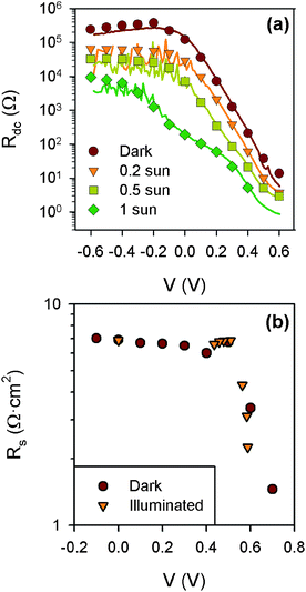 | ||
| Fig. 10 (a) Total cell resistance, Rdc, as a function of applied bias V. The solid line for each data set represents the Rdc value obtained from the derivative of the potential–current characteristic for each illumination respectively (small BP solar cell), and the points are obtained from impedance spectroscopy measurement. (b) Rs measured by impedance spectroscopy using two experimental configurations: (i) at dark applying different DC bias and (ii) under different illuminations applying a bias equal to Voc (small Isofoton solar cell). | ||
It can be seen that the Rdc obtained is analogous to that obtained from the current–potential characteristic, (dI/dV)−1. We remark that impedance characterisation allows to discriminate between the two contributions indicated in eqn (15). The small Isofoton solar cellRs has been measured using two experimental configurations, and the results are shown in Fig. 10(b): (i) at dark applying different DC bias with the Fermi level fixed by the applied bias and (ii) under different illuminations applying a bias voltage equal to Voc. In the latter case the illumination fixes the working conditions.12,13 The Rs values normalized by area present the same behaviour for both experimental conditions, indicating that series resistance depends of Fermi level position. That means that Rs should not be only ascribed to the connections leads, as we discuss below. On the other hand the variation of Rdc, see Fig. 10(a), by several orders of magnitude, is due to Rp variation. In this context Rp can be seen as a recombination resistance, its value will decrease as n increases, obtaining consequently decaying values as illumination intensity is increased.
As we have seen in Fig. 5, the reflecting back contact produces accumulation of electron minority carriers in the bulk, consequently the solar cell capacitance increases substantially. Note that for obtaining accurate results of the capacitance variation it is important to use the voltage VF which is a fraction of the total applied voltage V. To obtain VF we have subtracted the potential drop in Rs employing the current, I, measured in the current–potential characterisation at each experimental condition, considering that Rs behaves as an ohmic resistance:
| VF = V − IRs | (16) |
In Fig. 11(a), C is plotted as function of VF for different incident light intensities. The behaviour of C is divided in two regions, for high forward bias, VF > 0.4 V, capacitance increases exponentially with the absolute VF value, in this region C ≈ Cµ as described in eqn (6). It should be observed that Cµ remains invariant with respect to applied illumination intensity, and this is because the Fermi level position is fixed by the applied bias. An alternative measurement to analyze the role of illumination in the chemical capacitance is the measurement at zero current conditions under different illumination (applying a bias equal to Voc), as it has been commented elsewhere.12,13 In Fig. 10(b) the Rs presents a constant value (7 Ω cm2) for VF < 0.4 V, while for VF > 0.4 V its values decreases with the applied bias. This transit occurs at the same point at which C ≈ Cµ. When Cµ governs the capacitance of the device the density of minority carriers in the bulk region, outside depletion region, increases exponentially, see eqn (4) and (6). Consequently the conductivity of this region increases, reducing its resistance, as a consequence Rs is to be attributed mainly to the bulk part of the device.
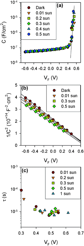 | ||
| Fig. 11 (a) Device capacitance as a function of Fermi-level potential, VF, for different light intensities. Solid line represents the fit of C in the potential region where Cµ is dominant. (b) Mott–Schottky C−2vs.VF plot, considering only the values of capacitance where Cdl is the main contribution to the cell capacitance (small BP solar cell). (c) Minority carrier lifetime as a function of Fermi level potential. | ||
Fitting the data in the region where C ≈ Cµ, see Fig. 11(a), to eqn (6), the diode factor can be calculated, η = 1.18, near the ideal unity value as should be expected from a good performance solar cell. From the product of C and Rp values the minority carrier lifetime can be calculated19 in the region of voltages where the capacitance is governed by the chemical capacitance (VF> 0.4 V). The results shown in Fig. 11(c) provide a nearly constant value of 10 µs for both kinds of cell, BP and Isofoton, when small samples are measured. The values obtained from the product of C and Rp at VF < 0.4 V have no physical meaning because in this region the cell capacitance is governed by the depletion capacitance. As Cµ scales linearly with cell area and Rp scales linearly with the inverse of the area, a constant value for the lifetime is expected independently of the cell area, but for complete cells a higher lifetime of 20 µs is obtained because complete cells have the edges passivated, while the small cells do not.
For reverse bias the behaviour of C with VF is smoother, and in this region C ≈ Cdl. Studying the Mott–Schottky plots of capacitance in this region, Fig. 11(b), it is possible, from the measurement in dark conditions, to obtain the acceptors density on p side of the cell, NA = 3.92 × 1016 cm−3. Under illumination it is assumed that additional carriers of each kind and in equal numbers, Δn = Δp, are added to each side of the junction. The additional majority carriers are assumed to be removed to form the depletion region, reducing the depletion region size. This leaves the ionised impurities plus the additional minority carriers, from light generation, ND + Δp and NA + Δn, to form the depletion region.34 Analysing the MS plots obtained under light illumination conditions, Fig. 11(b), the values of NA + Δn, considering NA + Δn << ND + Δp, can be calculated, for different light intensities. They are compiled in Table 1. The density of charge in the depletion region only improves by 20% for 1 sun illumination, and as a consequence the carrier density n in the bulk is mainly controlled by the applied bias rather than by illumination, explaining the similar behaviour of Cµ obtained from different illumination intensities, Fig. 11(a).
| Light Intensity (sun) | V 0 (V) | N A + Δn (NA) |
|---|---|---|
| 0 | 0.713 | 1.000 |
| 0.01 | 0.735 | 1.079 |
| 0.2 | 0.705 | 1.086 |
| 0.3 | 0.716 | 1.114 |
| 0.4 | 0.693 | 1.133 |
| 0.5 | 0.684 | 1.155 |
| 1 | 0.616 | 1.195 |
4. Conclusions
Impedance spectroscopy is a very powerful technique for solar cell characterization. We have employed this technique in the study of high performance silicon monocrystalline solar cells, relating the impedance pattern obtained with the theory of the impedance of electron diffusion and recombination in a semiconductor layer. Different cell parameters, as series and parallel resistances, capacitance, diode factor, minority carrier lifetime, acceptor impurities density and depletion layer charge density have been obtained as function of applied bias for different light illumination intensities. The behaviour of cell capacitance under illumination is determined by the applied bias rather than by the light carrier generation when measurement at fixed bias are carried out.Acknowledgements
The authors are grateful to BP-Solar Spain for providing solar cells. The work was supported by MEC project MAT2007-62982.References
- D. L. Losee, J. Appl. Phys., 1975, 46, 2204 CrossRef CAS.
- J. Bisquert, J. Phys. Chem. B, 2002, 106, 325 CrossRef CAS.
- F. Fabregat-Santiago, J. Bisquert, G. Garcia-Belmonte, G. Boschloo and A. Hagfeldt, Sol. Energy Mater. Sol. Cells, 2005, 87, 117 CrossRef CAS.
- F. Fabregat-Santiago, J. Bisquert, E. Palomares and J. R. Durrant, J. Appl. Phys., 2006, 100, 034510 CrossRef.
- Q. Wang, J.-E. Moser and M. Grätzel, J. Phys. Chem. B, 2005, 109, 14945 CrossRef CAS.
- T. Hoshikawa, R. Kikuchi and K. Eguchi, J. Electroanal. Chem., 2006, 588, 59 CrossRef CAS.
- M. Adachi, M. Sakamoto, J. Jiu, Y. Ogata and S. Isoda, J. Phys. Chem. B, 2006, 110, 13872 CrossRef CAS.
- Q. Wang, S. Ito, M. Grätzel, F. Fabregat-Santiago, I. Mora-Seró, J. Bisquert, T. Bessho and H. Imai, J. Phys. Chem. B, 2006, 110, 19406 CrossRef.
- G. Garcia-Belmonte, A. Munar, E. M. Barea, J. Bisquert, I. Ugarte and R. Pacios, Org. Electron., 2008, 9, 847 CrossRef CAS.
- J. Bisquert, G. Garcia-Belmonte, A. Munar, M. Sessolo, A. Soriano and H. J. Bolink, Chem. Phys. Lett., 2008, 465, 57 CrossRef CAS.
- L. Raniero, E. Fortunato, I. Ferreira and R. Martins, J. Non-Cryst. Solids, 2006, 352, 1880 CrossRef CAS.
- I. Mora-Seró, Y. Luo, G. Garcia-Belmonte, J. Bisquert, D. Muñoz, C. Voz, J. Puigdollers and R. Alcubilla, Sol. Energy Mater. Sol. Cells, 2008, 92, 505 CrossRef CAS.
- G. Garcia-Belmonte, J. García-Cañadas, I. Mora-Seró, J. Bisquert, C. Voz, J. Puigdollers and R. Alcubilla, Thin Solid Films, 2006, 514, 254 CrossRef CAS.
- Y. Y. Proskuryakov, K. Durose, B. M. Taele and S. Oelting, J. Appl. Phys., 2007, 102, 024504 CrossRef.
- R. Anil-Kumar, M. S. Suresh and J. Nagaraju, Sol. Energy Mater. Sol. Cells, 2000, 60, 155 CrossRef CAS.
- R. Anil-Kumar, M. S. Suresh and J. Nagaraju, Solar Energy, 2004, 76, 417 CrossRef.
- H. Bayhan and A. S. Kavasoglu, Solar Energy, 2000, 361, 303.
- J. Bisquert, D. Cahen, S. Rühle, G. Hodes and A. Zaban, J. Phys. Chem. B, 2004, 108, 8106 CrossRef CAS.
- I. Mora-Seró, J. Bisquert, F. Fabregat-Santiago, G. Garcia-Belmonte, G. Zoppi, K. Durose, Y. Y. Proskuryakov, I. Oja, A. Belaidi, T. Dittrich, R. Tena-Zaera, A. Katty, C. Lévy-Clement, V. Barrioz and S. J. C. Irvine, Nano Lett., 2006, 6, 640 CrossRef CAS.
- M. C. Morilla, M. J. Fernández, I. Antón, D. Pachón and G. Sala, in Proceedings of the 20th European PV Solar Energy Conference, Barcelona, Spain, 2005 Search PubMed.
- T. Burton, N. Mason, S. Roberts, O. N. Hartley, S. Gledhill, J. Femandez, R. Russell, W. Warta, S. Glunz, O. Schultz, M. Hermle and G. Willeke, in 3rd World Conference on Photovoltaic Energy Conversion, Osaka, Japan, 2003 Search PubMed.
- S. M. Sze, Physics of Semiconductor Devizes, John Wiley and Sons, New York, 1981 Search PubMed.
- J. Nelson, The Physics of Solar Cells, Imperial College Press, London, 2003 Search PubMed.
- J. Bisquert, Phys. Chem. Chem. Phys., 2003, 5, 5360 RSC.
- C.-T. Sah, Fundamentals of Solid State Electronics, World Scientific, Singapore, 1991 Search PubMed.
- E. A. Schiff, Sol. Energy Mater. Sol. Cells, 2003, 78, 567 CrossRef CAS.
- J. Bisquert, Phys. Rev. B, 2008 Search PubMed in press.
- J. Bisquert, Phys. Chem. Chem. Phys., 2008, 10, 3175 RSC.
- R. Brendel, Thin-film Crystalline Cilicon Colar Cells. Physics and Technology, Wiley -VCH Verlag, Wheinheim, 2003 Search PubMed.
- S. W. Glunz, Adv. Optoel., 2007, 97370 Search PubMed.
- J. Bisquert, G. Garcia-Belmonte, F. Fabregat-Santiago and P. R. Bueno, J. Electroanal. Chem., 1999, 475, 152 CrossRef CAS.
- J. Bisquert, Phys. Chem. Chem. Phys., 2000, 2, 4185 RSC.
- P. C. Ho Chan and C. T. Sah, IEEE Transactions on Electron Devices, 1979, ED-26, 924 CrossRef.
- W. B. Berry, Appl. Phys. Lett., 1974, 25, 195 CrossRef CAS.
| This journal is © The Royal Society of Chemistry 2009 |