Ultrathin Sb2S3nanowires and nanoplatelets†
R.
Malakooti‡§
a,
L.
Cademartiri‡
a,
A.
Migliori
b and
G. A.
Ozin
*a
aMaterials Chemistry and Nanochemistry Research Group, Lash Miller Chemical Laboratories, Department of Chemistry, University of Toronto, 80, St. George Street, Toronto, Ontario M5S 3H6, Canada. E-mail: gozin@chem.utoronto.ca
bCNR-IMM, Area della Ricerca di Bologna, via Gobetti 101, 40126, Bologna, Italy
First published on 26th September 2007
Abstract
Ultrathin (thickness < 2.2 nm) colloidal Sb2S3nanowires and nanoplatelets were synthesized via a simple solution synthesis. The nanowires and platelets were stable in solution for months and were characterized viaSAED, XRD, UV-VIS spectroscopy, SAXS, XPS and EDAX.
Introduction
The quest for nanoscale thermoelectric materials is luring more and more scientists from the field of materials chemistry.1 The promise is to create a material which would enable a device possessing enough thermoelectric efficiency to be competitive with modern refrigeration technologies and to allow efficient heat recovery as electrical current. Such ambition is well in line with the needs of a future of sustainable energy.Nanoscale thermoelectric elements have already demonstrated in theory and in practice the ability to substantially increase the thermoelectric figure of merit beyond what is achievable with the bulk counterparts,2,3 but still much work needs to be done in order to obtain nanostructures which possess the right characteristics. And these would be, according to theory, nanowires of the best thermoelectric compounds, with the smallest diameter possible.4,5 This would bring forth quantum confinement effects which would increase the density of states at the band edge (thus increasing the electrical conductivity) and increase the amount of surface area (thus decreasing the thermal conductivity due to boundary scattering).1 The simultaneous reduction of thermal conductivity and increase of electrical conductivity is the major requirement for thermoelectric performance. It is predicted theoretically though that in very specific cases excessively thin structures can display an increase of thermal conductivity, which was explained as an effect of phonon confinement.6
With this in mind we started our exploration of pnictide chalcogenide nanostructures. Pnictide chalcogenides are in fact the best thermoelectric materials known but are fairly unexplored when it comes to their reduction to the nanoscale;7–13 especially in the present case of Sb2S3nanostructures the exploration has been fairly limited. Qian's group reported nanowires between 20 and 100 nm in diameter14 while Son and coworkers very recently reported the solution synthesis of Sb2S3nanotubes15 obtained from rolled Sb2S3 layers.
In this work, we will show the synthesis of ultrathin Sb2S3 colloidal nanowires and nanoplatelets with a simple fast injection technique.
Experimental
All chemicals were purchased from Aldrich and used without further purification.Sb2O3 (3.4 mmol) was dispersed in 8.8 ml of 1-octadecene and 8.7 ml of oleic acid in a 50 ml three-necked flask equipped with a condenser and thermocouple held by a septum. The third neck of the flask was closed. The flask was flushed three times with N2 and then left under vacuum to remove water produced by the reaction between antimony oxide and the acid. The solution was stirred and heated to 200 °C in the course of 30 min and then kept at that temperature for 30 min, always under vacuum. The flask was then flushed with N2 and kept under inert conditions for the rest of the reaction. A solution of 34 mmol of sulfur dissolved in 33.6 ml of oleylamine was then swiftly injected into the flask. The solution turned orange immediately after injection and the nanostructures were allowed to grow for 5 min at 130 °C and then 5 min at 150 °C. The reaction was then quenched with 50 ml cold toluene. Unsolubilized materials were removed by centrifugation, and ethanol was added dropwise to the supernatant until it became turbid. The mixture was centrifuged, the supernatant discarded and the precipitated nanostructures re-dispersed in chloroform. This procedure was repeated twice to clean the nanostructures.
In order to separate the wires from the platelets a 5 ml solution of as prepared product was precipitated with 3 ml of ethanol. The precipitate consisted of nanowires.
Results and discussion
The obtained materials were imaged with STEM (Fig. 1).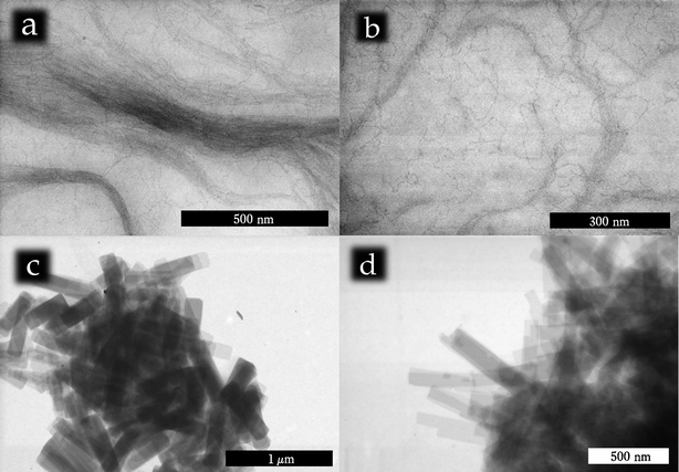 | ||
| Fig. 1 STEM analysis of Sb2S3 ultrathin nanowires and nanoplatelets: a) a bundle of colloidal Sb2S3nanowires; b) a higher magnification image of the Sb2S3nanowires which already allows appreciation of the degree of fragmentation of the nanowires due to the electron beam; c–d) STEM images of typical nanoplatelet assemblies. | ||
The typical diameter of the nanowires ranged between 1.8 and 2.2 nm. It is noteworthy that the wall thickness of the recently reported Sb2S3nanotube (1.8 nm) was very similar to this value.15 A precise measurement of the nanowire thickness and thickness distribution is complicated by the susceptibility of the wires to electron irradiation. The electron beam fragments the wires thus impeding a rigorous evaluation of the size as well as a thorough HRTEM analysis. Whatever product would be imaged in HRTEM would in fact probably be altered by the e-beam-induced degradation. For the same reasons it was impossible to measure a reliable number representing the length of the wires which was anyway well exceeding 1 μm.
The size of the platelets was widely varying (∼100 nm ×∼500 nm) but their shape was always found to be rectangular. Jagged edges and corners were found to be made exclusively of 90° angles testifying to their crystallinity and consistently with the orthorhombic symmetry of the Sb2S3 lattice. Also in this case, due to the fracturing of the platelets in solution and during sample preparation it is meaningless to attempt to calculate a number for the polydispersity as that would be inevitably incorrect. The pictures in Fig. 1c–d give a much more reasonable way to evaluate the uniformity of the platelets. The high uniformity in size is consistent with the possibility they might come from exfoliating Sb2S3 microcrystals. Larger Sb2S3 crystals were never observed but they were likely separated during the purification process. The growth medium of hot alkyl amines is consistent with this picture as amines are traditionally used as exfoliating agents.16 Moreover the layered nature of Sb2S3 has already been reported and used for example to fabricate inorganic nanotubes.15
The structural characterization had to be performed uniquely with SAED and XRD. SAED in fact allows electron diffraction data to be obtained at low magnification with no risk of damaging the sample. XRD, while at the limits of its reliability due the minuscule size of these nanostructures, can perform macroscopic average measurements which are obviously impossible for ED. No representative lattice imaging from HRTEM could be obtained under any imaging conditions due to the sensitivity of the material to e-beam irradiation.
In Fig. 2a you can observe an SAED pattern obtained from a bunch of Sb2S3nanowires. The crystalline nature is evident and the ring position is consistent with the lattice parameters of Sb2S3. In Fig. 2b the XRD pattern from Sb2S3nanowires shows the typical features of XRD patterns from ultrathin nanowires: some reflections, associated with planes perpendicular to the length of the wire, are sharp, while the reflections associated with planes across the wires are basically non-existent. Also, the crystal planes along which the nanowires grow shouldn't be visible since the nanowires are likely to be mostly lying down on the sample holder thus eliminating those reflections due to preferential orientation.
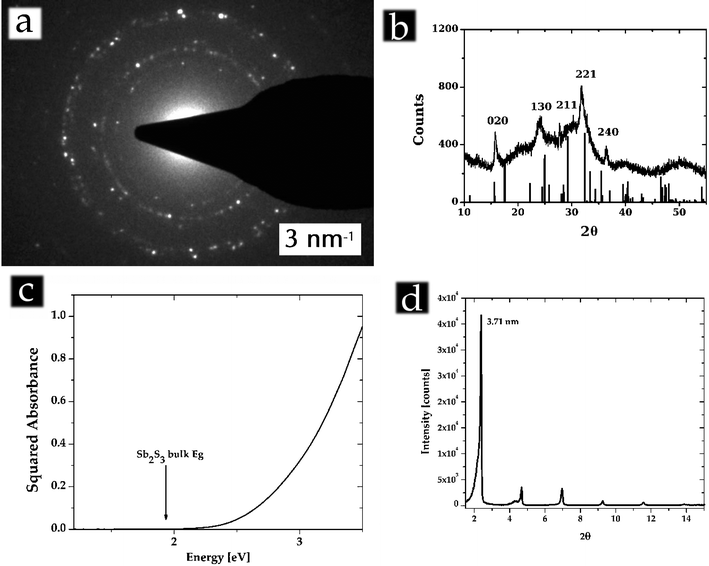 | ||
| Fig. 2 a) SAED pattern obtained from a number of Sb2S3nanowires; b) XRD pattern obtained from Sb2S3nanowires, compared with the bulk peaks; c) UV-VIS absorbance spectra (in units of squared absorbance), the position of the bulk bandgap is indicated with an arrow; d) SAXS data from an assembly of platelets. | ||
EDAX analysis gave an [Sb]/[S] ratio of 0.65 ± 0.39 which is consistent with Sb2S3 but also, in theory, with the less common Sb2S5. The synthesis conditions in excess of S make it very likely for S to be in excess on the surface thus altering sensibly the overall stoichiometry, without this meaning that the lattice structure or the Sb oxidation states are different from the Sb2S3 bulk structure. The XPS analysis (see electronic supplementary information (ESI)†) confirms this picture by showing the main Sb 3d5/2 peak at 529.71 which is perfectly consistent with an Sb3+ oxidation state and with a Sb2S3 lattice. The quantitative analysis from XPS also gave an [Sb]/[S] ratio of 0.74 which is consistent with EDAX and very close to the stoichiometric 0.67.
In Fig. 2c is plotted the optical absorbance of the nanowires (in units of squared absorbance vs. eV) evidencing the remarkable blue shift of the observed band-edge from the bulk band-edge. The featurelessness of the curve doesn't allow the conclusion that the observe blue shift is entirely due to quantum confinement effects as wide (∼0.6 eV) stoichiometry-induced shifts in the bandgap energy have been reported for the isostructural and more explored Bi2S3. The absence of excitonic features moreover does not allow testing of the consistency of the peak positions with effective mass approximation predictions. In such tiny structures stoichiometry becomes much more flexible than in bulk materials and that might account in itself for the blue-shift observed.
In Fig. 2d is shown instead the SAXS pattern obtained from assemblies of purified Sb2S3 nanoplatelets as shown in Fig. 1c–d. The remarkable emergence of a single set of extremely sharp peaks points to the long range order present in these assemblies which is a direct consequence of the uniformity in thickness of the platelets. From the first observed peak we calculate that the period length of such an ordered layered structure has to be 3.71 nm.
If we assume the platelets to be capped on their facets by oleylamine ligands and that such oleylamine ligands successfully interdigitate (as observed in other nanocrystal systems) then the platelet thickness results as being ∼1.8 nm which is very close to the thickness we measured from the parent wires and that was measured in nanotube walls.15
The ubiquity of this dimension strongly convinces us that it must correspond to some features in the Sb2S3 lattice.
In Fig. 3 we propose a possible structure for the wires. It is just a model which though seems to be the only one consistent with the measured nanowires size, the obtained characterization data and with the building blocks of the stibnite lattice. Sb2S3 (stibnite) is a layered structure composed of ribbons of composition [Sb4S6]n running along the c axis and kept together by weak interactions along the b axis.17 The layers, parallel to the ac plane, are corrugated due to the fact that the ribbons are not lying flat on them but at an angle. The shortest distances between atoms in different ribbons are 1.5 times larger than the equivalent distances within one ribbon. As shown in Fig. 3 the thickness of 3 layers of ribbons accounts for 1.6 nm and a nearly round nanowire section can be easily composed of 4 groups of a pair of ribbons in order to minimize the surface curvature. We exclude that the nanowires have a rectangular cross-section as no change in thickness along their length has been observed in the TEM. If these nanostructures were ribbon-like the inevitable twisting of the ribbons on the TEM grid would emerge as variations of thickness in the measured projection. The platelets could instead easily be formed by extending the structure shown in Fig. 3 along the b axis. This model also accounts for an excess of sulfur on the surface (Sb/S = 0.56 in the shown model) which would be consistent with the synthetic route. Given the extremely high percentage of atoms on the surface, the inevitable surface reconstruction, Laplacian pressure and lattice strain are likely to sensibly change the positions of the atoms and the quantitative accuracy of this model.
![Representation of Sb2S3 structure viewed along the [Sb4S6]n ribbons. The light grey spheres are Sb atoms while the dark grey spheres represent S atoms. The structure is visualized as a hypothesized wire cross-section, consistent with experimental data.](/image/article/2008/JM/b713383a/b713383a-f3.gif) | ||
| Fig. 3 Representation of Sb2S3 structure viewed along the [Sb4S6]n ribbons. The light grey spheres are Sb atoms while the dark grey spheres represent S atoms. The structure is visualized as a hypothesized wire cross-section, consistent with experimental data. | ||
It is for this reason that it is at this point premature to draw conclusions on the mechanism of formation of such wires and platelets. The remarkable uniformity in size of the wires and its constancy during growth hints at a possible oriented attachment mechanism, which is further supported by the highly anisotropic lattice structure of Sb2S3.
Conclusion
We have here presented a simple synthetic route which allows the reproducible synthesis of ultrathin Sb2S3nanowires and nanoplatelets. The colloidal nature of such nanostructures makes them amenable to solution processing and deposition on flexible substrates. The interest in thermoelectric materials with reduced dimensionality motivates this work and further encourages the exploration of synthetic routes towards thermoelectric nanostructures.Acknowledgements
G. A. O. is Canada Research Chair in Materials Chemistry. The authors are deeply indebted to NSERC for financial support. L. C. thanks the University of Toronto for a scholarship. R. M. thanks the Iranian Ministry of Science, Research and Technology for a scholarship and F. Farzaneh for support.Notes and references
- M. S. Dresselhaus, G. Chen, M. Y. Tang, R. G. Yang, H. Lee, D. Z. Wang, Z. F. Ren, J. P. Fleurial and P. Gogna, Adv. Mater., 2007, 19, 1043–1053 CrossRef CAS.
- R. Venkatasubramanian, E. Siivola, T. Colpitts and B. O'Quinn, Nature, 2001, 413, 597–602 CrossRef CAS.
- T. C. Harman, P. J. Taylor, M. P. Walsh and B. E. LaForge, Science, 2002, 297, 2229–2232 CrossRef CAS.
- L. D. Hicks and M. S. Dresselhaus, Phys. Rev. B, 1993, 47, R16631.
- T. E. Humphrey and H. Linke, Phys. Rev. Lett., 2005, 94.
- I. Ponomareva, D. Srivastava and M. Menon, Nano Lett., 2007, 7, 1155–1159 CrossRef CAS.
- M. B. Sigman, Jr. and B. A. Korgel, Chem. Mater., 2005, 17, 1655–1660 CrossRef CAS.
- E. J. Menke, Q. Li and R. M. Penner, Nano Lett., 2004, 4, 2009–2014 CrossRef CAS.
- C. G. Jin, X. Q. Xiang, C. Jia, W. F. Liu, W. L. Cai, L. Z. Yao and X. G. Li, J. Phys. Chem. B, 2004, 108, 1844–1847 CrossRef CAS.
- M. Martin-Gonzalez, G. J. Snyder, A. L. Prieto, R. Gronsky, T. Sands and A. M. Stacy, Nano Lett., 2003, 3, 973–977 CrossRef CAS.
- C. G. Jin, G. Q. Zhang, T. Qian, X. G. Li and Z. Yao, J. Phys. Chem. B, 2005, 109, 1430–1432 CrossRef CAS.
- R. Malakooti, L. Cademartiri, Y. Akcakir, S. Petrov, A. Migliori and G. A. Ozin, Adv. Mater., 2006, 18, 2189–2194 CrossRef CAS.
- J. Tang and A. P. Alivisatos, Nano Lett., 2006, 6, 2701–2706 CrossRef CAS.
- H. M. Hu, M. S. Mo, B. J. Yan, X. J. Zhang, Q. W. Li, W. C. Yu and Y. T. Qian, J. Cryst. Growth, 2003, 258, 106–112 CrossRef CAS.
- K. H. Park, J. Choi, H. J. Kim, J. B. Lee and S. U. Son, Chem. Mater., 2007, 19, 3861–3863 CrossRef CAS.
- T. Lan, P. D. Kaviratna and T. J. Pinnavaia, Chem. Mater., 1995, 7, 2144–2150 CrossRef CAS.
- S. Scavnicar, Z. Kristallogr., 1960, 114, 85 CAS.
Footnotes |
| † Electronic supplementary information (ESI) available: HR XPS spectra of the Sb 3d5/2 peaks. See DOI: 10.1039/b713383a |
| ‡ These authors contributed equally to the work. |
| § On leave from Department of Chemistry, University of Birjand, Birjand, South Khorasan, Iran. |
| This journal is © The Royal Society of Chemistry 2008 |