Optically addressable single molecule magnet behaviour of vacuum-sprayed ultrathin films†
Riccardo
Moroni
a,
Renato
Buzio
a,
Andrea
Chincarini
b,
Ugo
Valbusa
a,
Francesco Buatier
de Mongeot
*a,
Lapo
Bogani
c,
Andrea
Caneschi
c,
Roberta
Sessoli
*c,
Lucia
Cavigli
d and
Massimo
Gurioli
d
aDipartimento di Fisica and CNISM, Università di Genova, 16146, Genova, Italy. E-mail: buatier@fisica.unige.it
bINFN, Sezione di Genova, 16146, Genova, Italy
cLa.M.M. and INSTM research unit, University of Florence, Via della Lastruccia 3, 50019, Sesto Fiorentino (Fi), Italy. E-mail: roberta.sessoli@unifi.it; Fax: +39-0554573372; Tel: +39-0554573268
dL.E.N.S., University of Florence, Via N. Carrara 1, 50019, Sesto Fiorentino (Fi), Italy
First published on 8th November 2007
Abstract
Films of the molecular nanomagnet Mn12ac with thicknesses spanning the nm to μm range have been deposited using a customised vacuum spray deposition technique. The films have been characterized by AFM, XPS, magnetic and magneto-optical measurements, indicating that the deposition procedure does not damage the Mn12ac molecules. As a result, the films show magnetic properties similar to those of the parent molecular material down to the nm thickness range, as revealed by magneto-optical methods. Vacuum spray deposition therefore represents a promising approach for the preparation under controlled vacuum conditions of ultrathin films of molecular nanomagnets supported on transparent dielectric substrates, making possible the magneto-optical readout of the magnetisation state of the Mn12ac film.
Introduction
In the past ten years paramagnetic molecules characterized by a large ground spin state and a strong easy-axis magnetic anisotropy have been widely investigated because they show magnetic hysteresis without long-range magnetic order.1 This phenomenon is due to the fact that the relaxation time of the magnetisation for each single molecule follows a thermally-activated law and becomes extremely long at low temperatures. Each molecule then behaves as a single-domain magnetic particle and thus they have been attributed the evocative name Single Molecule Magnets (SMMs).2 The interest in this novel class of magnetic materials resides in their complex behaviour that combines classic features, like the hysteresis loop, to quantum effects,3 like the Landau–Zener tunneling of the magnetisation4 and the topological interference of the tunnel pathways.5 Thanks to these features SMMs have been proposed for a number of possible future applications, as ultra-high density magnetic recording media or quantum-bits for logic devices.6 Recently their quantum properties have attracted great attention also for magneto-electronic systems in the emerging field of molecular spintronics where SMMs seem to be extremely appealing candidates for single molecule addressing in break-junction devices7 or in the novel nanoSQUID junctions.8 As the full exploitation of the potentiality of SMMs in such systems requires the addressing of individual molecules, several studies to organise them at the nanoscale have appeared in the past few years. These attempts have been mainly focused on the archetypal SMM [Mn12O12(CH3COO)16(H2O)4]·2CH3COOH·4H2O, Mn12ac.9This dodecanuclear mixed-valence manganese cluster, whose structure is schematized in Fig. 1, comprises four Mn(IV) and eight Mn(III) ions, bridged by oxide and carboxylate ligands. These last ones can be easily exchanged with other carboxylates or bidentate ligands,10 and this feature has been exploited either to functionalize the cluster to graft it on native gold substrates11 to form a Self Assembled Monolayer (SAM) or to graft the cluster on a surface (Au or Si) pre-functionalized with a SAM of carboxylate groups.12 Several reports on the deposition of monolayers on Au or Si have recently appeared, but in many cases a significant modification of the redox state13 or of the magnetic properties14 has been observed.
![Molecular structure of [Mn12O12(CH3COO)16(H2O)4] with the manganese atoms represented by large grey spheres, oxygen atoms by black spheres and carbon ones by small grey spheres. Hydrogen atoms of the methyl groups and crystallization molecules of water and of acetic acid are not shown for the sake of clarity.](/image/article/2008/JM/b712913k/b712913k-f1.gif) | ||
| Fig. 1 Molecular structure of [Mn12O12(CH3COO)16(H2O)4] with the manganese atoms represented by large grey spheres, oxygen atoms by black spheres and carbon ones by small grey spheres. Hydrogen atoms of the methyl groups and crystallization molecules of water and of acetic acid are not shown for the sake of clarity. | ||
All the aforementioned examples require solution-based techniques and this prevents their use in combination with in situ ultra-high vacuum (UHV) deposition techniques, particularly useful for the creation of multilayer nanostructures based on SMMs, which represent the fundamental building block of present and future devices. Moreover, at variance with solution-based chemical deposition techniques, UHV-compatible physical deposition techniques do not rely on the chemical properties of the surface, allowing for less restricted choice of the substrates. This last issue is particularly relevant for the creation of SMM-based magneto-optical (MO) devices where the organisation of SMMs onto substrates with proper optical properties may lead to the creation of multifunctional MO materials exploiting their unusual magnetic properties and allowing the addressing and/or the manipulation of the magnetic information by optical means.
In this respect, previously reported attempts of depositing SMMs by physical methods had only partial success. Thermal evaporation of Mn12 materials is not feasible due to thermal lability of the compounds. Alternative techniques, like pulsed laser deposition (PLD)15 or matrix-assisted pulsed laser evaporation (MAPLE),16 have been used. The second strategy seems to provide films of better quality, but in both cases a significant fraction of the molecules appear to be fragmented, as evidenced by the presence of a magnetic phase that strongly resembles the Hausmannite phase of Mn3O4, a common by-product in the degradation of manganese clusters.17 From this perspective, the exploration of alternative deposition routes, able to provide deposition of films in the nanometre thickness regime of unaltered Mn12 clusters under controlled vacuum conditions is very important for the further development of this promising research field.
To this aim we implemented a novel custom-made set-up for the deposition of SMM films in a vacuum chamber through direct injection of a spray containing a solution of the SMM (see Experimental for details). For our study we have focused on the archetype Mn12ac, due to the fact that it displays one of the highest blocking temperatures and that previous attempts were also based on this molecule. In the following we show that this novel deposition technique allows the preparation of thin SMM films with an accurate control of their thickness down to the nanometre range. Films of Mn12ac have been deposited on different substrates and characterized by atomic force microscopy (AFM), X-ray photoelectron spectroscopy (XPS), magnetic and magneto-optical measurements. Quantitative analyses of the XPS spectra of the Mn12ac powders and of the as-deposited films allow the assignment of the observed photoemission features, providing evidence that no degradation of Mn12ac molecules takes place in the film. This result is also confirmed by the reported magnetic measurements, conducted by standard vibrating sample and SQUID magnetometry, providing direct evidence that the magnetic features of the SMMs are preserved also for thin films. More interestingly, in view of application in MO devices, we also show that it is possible to prepare optical quality nanometre-thick Mn12ac films preserving the magnetic behaviour of the SMMs and addressable by the use of a MO set-up sensitive to the magnetic circular dichroism of the film.
Results and discussion
AFM characterization
The morphology of the films grown by vacuum spray deposition has been investigated by means of non-contact AFM measurements18 (Park Instruments). The thickness of the deposited films is monitored during deposition by means of a quartz-crystal microbalance (QCM). The frequency shift of the quartz was correlated to the actual thickness of the film by means of AFM measurements on scratched samples (as shown in Fig. 2a). As substrates we chose LiF(001) cleaved immediately prior to introduction into the deposition chamber, since this substrate ensures a very low initial roughness.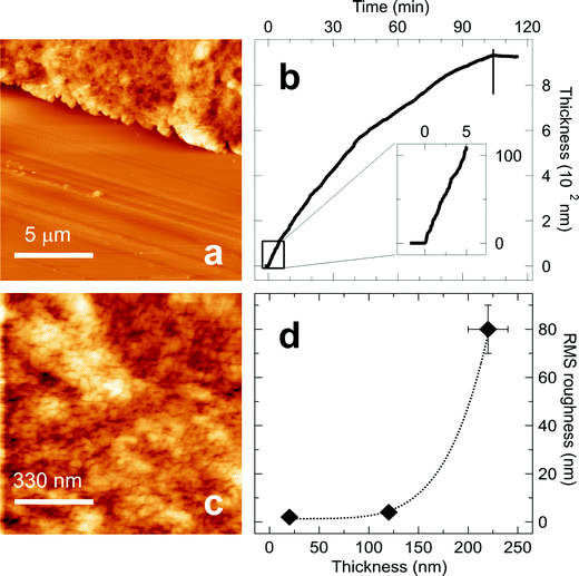 | ||
| Fig. 2 Morphological characterization of the sample. (a) AFM image (vertical range 476 nm) of a scratched sample used for calibrating the QCM reading. (b) Calibrated QCM uptake curve recorded during deposition. The inset shows an expanded view of the QCM uptake curve in the low-thickness region. The vertical scale of the inset is expressed in nm. (c) AFM image (vertical range 13 nm) showing the morphology of the 120 nm thick Mn12ac film deposited on LiF(001). (d) Evolution of rms roughness as a function of film thickness. The line is a guide for the eye. Error bars for film thickness below 150 nm are smaller than the marker size. | ||
In Fig. 2b a typical QCM uptake curve during deposition is shown. The thickness of the deposited films grows regularly during the operation of the source and can be controllably scaled down to the 10 nm range (see inset). Optical microscopy analysis of the deposited films shows that the films are continuous and uniform except for less regular portions, which amount to about 20% of the whole film area and are probably due to excess solvent reaching the substrate during spray deposition.
AFM images acquired in macroscopically uniform regions show the formation of continuous films. No preferential nucleation of extended crystalline domains is observed in the AFM images. On the other hand, the present results cannot provide conclusive evidence about the occurrence of short-range crystallization in regions of size below the lateral resolution of the AFM tipi.e. about 10 nm. Films with a thickness above 150 nm exhibit a significant average root mean square (rms) roughness. In Fig. 2a we report the morphology of a typical 220 nm thick Mn12ac film showing an rms roughness of about 80 nm. Such a roughness is sufficient for most optical operations, but certainly hinders the creation of optical devices, where a significantly improved quality of the surface is necessary. In order to check whether films of improved morphological properties could be obtained, in particular concerning the rms roughness, we investigated the growth of Mn12ac overlayers in the nanometre thickness regime. Fig. 2c (scan size 1 μm × 1 μm) represents the AFM morphology of a 120 nm thick Mn12ac film, which reveals a significantly reduced rms roughness of about 4 nm. The film morphology is dominated by aggregation of small Mn12ac clusters with diameters comparable to or smaller than the tip curvature radius (i.e. less than 10 nm). As revealed by statistical analysis of AFM images corresponding to films of different thickness (Fig. 2d), relatively smooth Mn12ac overlayers (rms roughness in the nm range) are grown for thicknesses just below 150 nm, while a remarkable increase of the rms roughness is observed for thicker films. These results indicate that vacuum spray deposition is an effective alternative for the growth of molecular nanomagnet films of controlled morphology in the nanometre thickness range thus providing a way to achieve films endowed with an optical quality otherwise unavailable with other techniques. We stress here that the relative residual rms roughness of the Mn12ac films grown by vacuum spray deposition is significantly low and corresponds to about four molecular diameters. This figure is of the same order of magnitude of the typical height distribution observed in molecular beam epitaxy (MBE) growth of metallic films at similar thicknesses and temperatures, where, even in the case of homoepitaxial growth, an unavoidable residual roughness in the growth front appears due to the presence of kinetically induced roughening and restricted thermally-activated diffusion.19 The low roughness observed in the thinner Mn12ac films is thus a particularly relevant result because, given the thermal lability of the Mn12ac compounds, it is not possible to improve the flatness and crystallinity of the films by thermal annealing cycles.
XPS characterization
XPS experiments have been performed ex situ on Mn12ac films grown on conductive Al substrates in order to ensure proper grounding. Reference spectra of the parent molecular material have been obtained by pounding Mn12ac powders into an In foil. Since pounding into the In foil does not provide sufficient grounding, a neutralizer was operated during the acquisition of the XPS spectra of the powder sample in order to prevent charging of the crystallites. In the survey XPS spectra of both the powder and film samples, with the exception of the chemical species present in the Mn12ac (i.e.Mn, O, and C), no traces of contaminants were detected. In the case of the film, the absence of N peaks rules out the presence of residual acetonitrile solvent in the film.In Fig. 3 we show the C1s, O1s and Mn2p core-level spectra of the reference powder sample (upper panels) and the film (lower panels). Vertical axes are scaled to allow direct comparison of the corresponding peaks of the two samples on a “per-Mn-ion” basis.
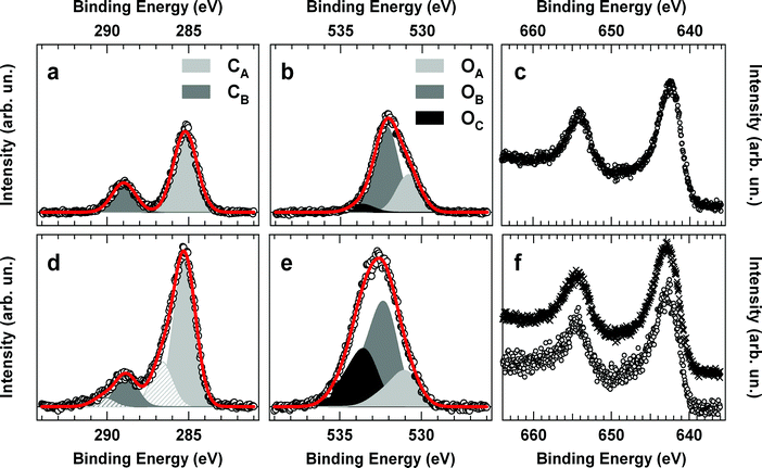 | ||
| Fig. 3 XPS spectra of the C1s (left panels), O1s (middle panels) and Mn2p (right panels) regions for a powder sample of Mn12ac (top panels) and for a Mn12ac film on Al foil (bottom panels). In panel d, the principal (shaded) and satellite (hatched) peaks are also shown. In the panel f, the film (○) and the corrected powder spectra (×) are shown. See text for details. | ||
The analysis of the C1s signal of the powder sample (panel a) reveals the presence of two main Gaussian peaks of equal FWHM (1.6 eV) at 285.2 eV (CA) and 289 eV (CB). We assign CA to the methyl group and to the presence of adventitious carbon, i.e.carbon mainly due to amorphous hydrocarbons ubiquitous in ex situ prepared substrates. CB is assigned to the carboxylic carbon of acetate ligands and acetic acid molecules. The observed C1s signal agrees well with the one reported in ref. 15 but, at variance with the one of ref. 20, no shoulder at low binding energy (BE) was observed. This discrepancy might be attributed to charging effects due to the insulating nature of the single crystal sample used in ref. 20. With regard to the O1s spectral region, reported in panel b of Fig. 3, the powder spectrum is characterized by the presence of a broad asymmetric peak. As in the case of the C1s spectral region, we do not observe the low BE shoulder observed in ref. 20, while good agreement with spectra reported in ref. 15 is obtained. Three Gaussian functions (FWHM = 1.7 eV) were used to fit the experimental data. The maxima of the Gaussian functions are located at 530.8 eV (OA), 532.2 eV (OB) and 533.7 eV (OC). The peak binding energies of OA and OB agree with the peaks already observed in ref. 20 and correspond to oxygen atoms acting as μ-oxo bridges and carboxylate oxygens, respectively. The high BE peak (OC) is assigned to water molecules. The assignment of CB and OB peaks to carboxylic carbon and oxygen atoms is also supported by the comparative analysis of the intensity of the two peaks, which affords a C to O relative atomic ratio of 1 : 2, as expected for the carboxylic group. In panel c of Fig. 3, the Mn2p doublet is shown. Due to the relatively small chemical shift observed for Mn ions in different valence states,21 no attempt to resolve the peaks corresponding to Mn(III) and Mn(IV) in Mn12ac was made. The maximum of the Mn2p3/2 peak was found at a BE of 642.3 eV, in agreement with the mixed-valence state of the Mn ions in the Mn12ac molecule.
In the bottom panels of Fig. 3, the XPS data for the film of Mn12ac are shown. At variance with the case of the powder sample, XPS spectra were recorded without the neutralizer. In fact, the close contact with the conducting Al substrate ensures efficient grounding of most parts of the film thus allowing a direct calibration of the energy scale and also minimizing possible damage of the molecules by low-energy electrons. The presence of insulating domains induces however satellite peaks, shifted by about 1.5 eV and with intensity corresponding to about one third of the principal peak (panel d), whose presence was taken into account in the analysis.
As shown in Fig. 3 (panel d), the C1s signal of the film was fitted with two pairs of Gaussian functions (principal and satellite peaks) corresponding to the methyl group and adventitious carbon (CA), and the carboxylic group (CB). Proceeding analogously to the analysis of the C1s signal, the O1s signal was fitted with three pairs of Gaussian functions (panel e). The analysis reveals the presence of oxygen in μ-oxo bridges, carboxylic groups and water molecules, in agreement with the analysis of the powder sample. With regard to the Mn2p signal, in order to compare the film and powder spectra, the latter has been corrected by including the contribution of insulating domains (panel f). This correction has been performed by adding to the original powder spectrum the same powder spectrum shifted in energy and scaled according to the energy position and intensity of satellite peaks observed in the C1s and O1s spectral regions.
Comparison of the powder and film XPS data sets reveals the presence of larger amounts of adventitious carbon and water molecules in the film spectra, an observation which is not surprising for films in the tens of nanometres thickness range due to the high surface/volume ratio. Apart from this, the analysis of the Mn2p spectral region and the agreement between the film and the corrected powder spectra indicate that no change occurred in the valence state of the Mn ions. In particular, at variance with more energetic laser-based deposition techniques,16 no shift of the Mn2p is observed and the formation of relevant quantities of Hausmannite can be excluded due to the lack of the Mn(II) shake-up satellites (BE = 645.5 eV) observed in Mn3O421 and heated Mn12ac.22
These findings suggest that the vacuum spray technique can be used as an alternative to solution methods23, 24 to deposit intact Mn12 molecules assembled into supported films. It represents a promising approach for the preparation of SMM films which preserve the properties of the parent molecular material, at variance with more energetic deposition techniques such as thermal evaporation, PLD and MAPLE. In particular, the relatively low energy involved in these experiments suggests that the energy scale implied by the deposition technique is of paramount importance for the preservation of the SMM behaviour.
Magnetic characterization
In order to test that the films exhibit the same peculiar magnetic properties as the Mn12ac molecules, we performed magnetic characterization of the samples using different instrumental set-ups. In order to compare with available reference data based on standard vibrating sample and SQUID magnetometry, which require a significant amount of magnetic material to provide reliable data, we have prepared films with thicknesses in the micrometre regime. Cleaved LiF(001) substrates have been chosen because they exhibit a low residual magnetic signal, an essential feature for detecting the weak signal originating from the thin Mn12ac films. Moreover the optical transparency and low roughness of the LiF substrate allows checking of the desired multifunctionality of the materials by performing MO measurements in transmission mode.Zero field cooled (ZFC) and field-cooled (FC) measurements in a field of 500 Oe have been performed to assess the presence of irreversibility, typical of Mn12ac. In Fig. 4, the magnetisation of a 1 μm thick Mn12ac film measured with a SQUID magnetometer is shown as a function of temperature. The measured magnetisation values agree with that expected for this film thickness. A clear irreversibility is observable below 2.75 K, which compares well with the blocking temperature (TB) previously observed for Mn12ac, and attributed to the characteristic slowing down of the relaxation of pure molecular origin without any cooperative effect.1,25 Above TB the sample has a paramagnetic behaviour with no evidence of the Hausmannite phase detected in ref. 15 and 16.
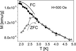 | ||
| Fig. 4 Temperature dependence of the magnetisation of a 1 μm thick Mn12ac film on LiF(001). The measurement is reported per gram of sample (LiF + Mn12ac) and is performed by cooling in zero field (grey triangles) and cooling in the applied field of 500 Oe (black circles) was used for both measurements. Lines are guides to the eye. | ||
The magnetisation has then been measured as a function of the applied magnetic field with the SQUID magnetometer. As shown in Fig. 5 (open circles), the opening of a hysteresis loop at low temperatures has been observed. The same measurements have been performed with an Oxford Instrument Vibrating Sample Magnetometer (VSM) which allows uniform fast ramping of the field at controllable sweep rates.26 The comparison of the two measurements confirms the typical sweep rate and temperature dependence of the hysteresis loop. The large steepness observed in zero field suggests the presence of faster relaxing clusters, as are often observed in the crystal phase of most Mn12 derivatives and attributed to the flipping of the Jahn–Teller elongation axis of a Mn(III).27 The small amount of magnetic material on the thick substrate has not allowed a characterization through ac susceptibility.
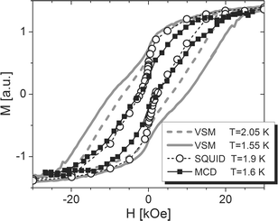 | ||
| Fig. 5 Field dependence of the magnetisation of 1 μm thick Mn12ac film on LiF(001) measured with a SQUID magnetometer at small sweep rate (<5 Oe s−1) (open circles) and with a VSM at the sweeping rate of 167 Oe s−1 and at 1.55 K (grey line) and 2.05 K (grey dashed line). MCD signal (solid squares) of a 20 nm thick film recorded with the same sweeping rate. The data have been linearly corrected for the diamagnetic contribution of the substrate and for the contribution of the optical components. | ||
We have then directly probed the multifunctional properties of the material by optically addressing the magnetisation of the films. In the present case the magnetisation state has been deduced by the dichroic signal, defined as the difference between the absorption coefficients of the right and left circularly polarised light, which was recorded at 1.6 K as a function of the magnetic field, swept at 167 Oe s−1.
The poor optical quality of the 1 μm thick film resulted in excessive light scattering due to the roughness of its surface, thus preventing the characterization of the sample by the MO technique. It is then evident that the control of the roughness achieved with the deposition technique is of fundamental importance in view of application in SMM-based magneto-optical devices. On the contrary the very low roughness achieved for thin films (see Fig. 2), allowed the MO characterization of the samples, indicating that the vacuum spray deposition technique can afford systems of sufficient quality for the future development of SMM-based heterostructures suitable for optical applications. In Fig. 5 (open circles), we report the results obtained for a 20 nm thick film, which would be otherwise undetectable with standard magnetometric techniques. The opening of the hysteresis is clearly visible. The observed coercive field Hc = 2.3 kOe, is however smaller than that measured with the VSM instrument operating at the same sweeping rate. These discrepancies between inductive and optical measurements are to be assigned to the different measuring techniques employed. In fact, using the MO techniques, depending on the employed wavelength, different parts of the absorption spectrum characterized by different polarisation of the electronic transitions are monitored. From reported data a reduced coercive field can be expected for a Mn12ac sample at the wavelength used.28
Conclusions
Summing up, we have demonstrated that fabrication of Mn12ac films, with thicknesses spanning the nm to μm range, can be achieved by means of vacuum spray deposition. In the thickness range from 10 to 100 nm, the technique allows films to be grown with very low rms roughness. At variance with previously reported deposition techniques that rely on more energetic methods and have revealed partial degradation of the clusters, the present vacuum spray technique allows the deposition of unaltered Mn12ac molecules. The chemical integrity of the Mn12ac molecules has been assessed by quantitative XPS analysis of the films and of the reference powders. Correspondingly, the fingerprint SMM behaviour of Mn12ac has been observed both in the thick as well as in the thin-film regime by standard and magneto-optical magnetometry. These results open the perspective to extend this vacuum compatible technique for in situ preparation of supported (sub)monolayers of SMMs as well as for the fabrication of multilayered nanostructures combining magnetic or conducting layers with thin film of SMMs. More important for potential applications appears the possibility to use the vacuum spray technique to grow high quality, nanometre-thick, SMMs films supported on transparent dielectric substrates whose magnetisation state can be addressed by adopting magneto-optical detection schemes.Experimental
Sample preparation
Microcrystalline powders of Mn12ac have been prepared following the literature9 and magnetically characterized before their use in the deposition experiments. For the preparation of Mn12ac films a saturated solution of Mn12ac in acetonitrile was used.The custom-made deposition source consists of a reservoir containing the solution, separated from the vacuum chamber by a fast-acting pulsed valve with a nozzle diameter of 0.8 mm.29 The vacuum chamber is pumped by a 70 l s−1 turbo-molecular pump and has a base pressure of the order of 1 × 10⁻⁷ mbar. At the opening of the valve, a pulsed beam of spray is injected into the vacuum chamber. The solvent droplets behave as carriers for the dissolved SMM molecules. After the valve, a focusing nozzle is inserted in order to focus the expanding beam onto the substrate. The focusing nozzle allows a uniform deposition rate to be obtained over a spot of about 1 cm in diameter and increases the flux by a factor of four with respect to the unfocused beam. The focused beam is led along a 30 cm long heated flight tube in order to enhance solvent evaporation. The temperature of the flight tube is stabilised at about 80 °C in order to prevent thermal fragmentation of the Mn12ac molecules.30 The valve is operated with pulses of 500 μs at a frequency of 0.1 Hz. During the operation of the valve, the average pressure rises up to the 1 × 10⁻³ mbar range. The films have been deposited onto high-purity Al foils for XPS measurements while for AFM measurements and magnetic characterization we have used LiF substrates obtained by a single crystal freshly cleaved along the (001) planes and rapidly inserted into the vacuum chamber.
Sample characterization
XPS measurements have been performed ex situ using a Perkin-Elmer PHI 5602 CI system with monochromatic Al Kα source (hν = 1486.6 eV). Spectra of the pristine molecular materials have been obtained by pounding the powders into an In foil. Since pounding does not provide sufficient grounding, a neutralizer was operated during the acquisition of the XPS spectra of the powder samples in order to prevent charging of the crystallites.The morphology of the evaporated films has been investigated by means of non-contact AFM measurements (Autoprobe CP, Park Instruments). Operation of the AFM in contact mode was avoided in order to prevent the modification of the film morphology due to tip–surface interactions.
The magnetic properties have been characterized using a Cryogenic S600 SQUID magnetometer and a vibrating sample magnetometer based on the MAGLAB2000 Oxford Instrument platform.
The magneto-optical characterization has been performed with a homemade MO set-up described in detail elsewhere.31 We briefly report here its salient characteristics for convenience. It allows reaching temperatures down to 1.5 K and high-fields (up to 115 kOe), with a maximum sweep rate of 167 Oe s−1. During the measurement the sample is kept immersed in superfluid He and all measurements were performed using a monochromatic laser light at a wavelength of 632.8 nm, generated by a stabilised He–Ne Melles Griot laser source. The dichroic signal, defined as the difference between the absorption coefficients of the right and left circularly polarised light, is recorded as a function of the magnetic field. To increase the sensitivity the incoming beam passes through a photo-elastic modulator (PEM), placed in front of the sample, which modulates its polarisation state at a frequency of 50 kHz. The signal is then recorded using a lock-in amplifier.
Acknowledgements
The financial support of Italian MIUR through PRIN 2005 and FIRB04-RBNE-033KMA projects and of EC for NMP3-CT-2005-515767 MAGMANet funds are acknowledged. Technical assistance from G. Firpo is acknowledged.References
- D. Gatteschi, R. Sessoli and J. Villain, Molecular Nanomagnets, Oxford University Press, Oxford, 2006 Search PubMed.
- G. Christou, D. Gatteschi, D. N. Hendrickson and R. Sessoli, MRS Bull., 2000, 25, 66 CAS.
- D. Gatteschi and R. Sessoli, Angew. Chem., Int. Ed., 2003, 42, 268 CrossRef CAS.
- (a) J. R. Friedman, M. P. Sarachik, J. Tejada and R. Ziolo, Phys. Rev. Lett., 1996, 76, 3830 CrossRef CAS; (b) L. Thomas, F. Lionti, R. Ballou, D. Gatteschi, R. Sessoli and B. Barbara, Nature, 1996, 383, 145 CrossRef CAS.
- W. Wernsdorfer and R. Sessoli, Science, 1999, 284, 133 CrossRef CAS.
- M. N. Leuenberger and D. Loss, Nature, 2001, 410, 789 CrossRef CAS.
- (a) H. B. Heersche, Z. De Groot, J. A. Folk, H. S. J. Van Der Zant, C. Romeike, M. R. Wegewijs, L. Zobbi, D. Barreca, E. Tondello and A. Cornia, Phys. Rev. Lett., 2006, 96, 206801 CrossRef CAS; (b) M. H. Jo, J. E. Grose, K. Baheti, M. M. Deshmukh, J. J. Sokol, E. M. Rumberger, D. N. Hendrickson, J. R. Long, H. Park and D. C. Ralph, Nano Lett., 2006, 6, 2014 CrossRef CAS.
- J.-P. Cleuziou, W. Wernsdorfer, V. Bouchiat, T. Ondrarçuhu and M. Monthioux, Nature Nanotechnol., 2006, 1, 53 Search PubMed.
- T. Lis, Acta Crystallogr., Sect. B, 1980, 36, 2042 CrossRef.
- (a) H. J. Eppley, H.-L. Tsai, N. de Vries, K. Folting, G. Christou and D. N. Hendrickson, J. Am. Chem. Soc., 1995, 117, 301 CrossRef CAS; (b) M. Soler, P. Artus, K. Folting, J. C. Huffman, D. N. Hendrickson and G. Christou, Inorg. Chem., 2001, 40, 4902 CrossRef CAS; (c) P. Artus, C. Boskovic, J. Yoo, W. E. Streib, L. C. Brunel, D. N. Hendrickson and G. Christou, Inorg. Chem., 2001, 40, 4199 CrossRef CAS.
- (a) A. Cornia, A. C. Fabretti, M. Pacchioni, L. Zobbi, D. Bonacchi, A. Caneschi, D. Gatteschi, R. Biagi, U. Del Pennino, V. De Renzi, L. Gurevich and H. S. J. Van Der Zant, Angew. Chem., Int. Ed., 2003, 42, 1645 CrossRef CAS; (b) L. Zobbi, M. Mannini, M. Pacchioni, G. Chastanet, D. Bonacchi, C. Zanardi, R. Biagi, U. Del Pennino, D. Gatteschi, A. Cornia and R. Sessoli, Chem. Commun., 2005, 1640 RSC; (c) A. Naitabdi, J.-P. Bucher, P. Gerbier, P. Rabu and M. Drillon, Adv. Mater., 2005, 17, 1612 CrossRef CAS; (d) S. Phark, Z. G. Khim, B. J. Kim, B. J. Suh, S. Yoon, J. Kim, J. M. Lim and Y. Do, Jpn. J. Appl. Phys., 2004, 43, 8273 CrossRef CAS.
- (a) G. G. Condorelli, A. Motta, I. L. Fragala, F. Giannazzo, V. Raineri, A. Caneschi and D. Gatteschi, Angew. Chem., Int. Ed., 2004, 43, 4081 CrossRef CAS; (b) J. S. Steckel, N. S. Persky, C. R. Martinez, C. L. Barnes, E. A. Fry, J. Kulkarni, J. D. Burgess, R. B. Pacheco and S. L. Stoll, Nano Lett., 2004, 4, 399 CrossRef CAS; (c) B. Fleury, L. Catala, V. Huc, C. David, W. Z. Zhong, P. Jegou, L. Baraton, S. Palacin, P. A. Albouy and T. Mallah, Chem. Commun., 2005, 2020 RSC.
- (a) M. Mannini, D. Gatteschi, R. Sessoli, L. Zobbi, A. Cornia, C. C. dit Moulin, P. Sainctavit and J.-P. KapplerBESSY Highlights 2005, Berliner Elektronenspeicherring-Gesellschaft für Synchrotronstralung m.b.H – BESSY, Berlin, Germany, p. 14, available from http://www.bessy.de/publicRelations/publications/files/Highlights2005.pdf Search PubMed; (b) S. Voss, M. Fonin, U. Rudiger, M. Burgert, U. Groth and Y. S. Dedkov, Phys. Rev. B, 2007, 75, 133104.
- (a) A. N. Abdi, J. P. Bucher, P. Rabu, O. Toulemonde, M. Drillon and P. Gerbier, J. Appl. Phys., 2004, 95, 7345 CrossRef CAS; (b) Z. Salman, K. H. Chow, R. I. Miller, A. Morello, T. J. Parolin, M. D. Hossain, T. A. Keeler, C. D. P. Levy, W. A. MacFarlane, G. D. Morris, H. Saadaoui, D. Wang, R. Sessoli, G. G. Condorelli and R. F. Kiefl, Nano Lett., 2007, 7, 1551 CrossRef CAS.
- J. Means, V. Meenakshi, R. V. A. Srivastava, W. Teizer, A. Kolomenskii, H. A. Schuessler, H. Zhao and K. R. Dunbar, J. Magn. Magn. Mater., 2004, 284, 215 CrossRef CAS.
- V. Meenakshi, W. Teizer, D. G. Naugle, H. Zhao and K. R. Dunbar, Solid State Commun., 2004, 132, 471 CrossRef CAS.
- A. L. Barra, A. Caneschi, D. Gatteschi, D. P. Goldberg and R. Sessoli, J. Solid State Chem., 1999, 145, 484 CrossRef CAS.
- Operation of the AFM in contact mode was avoided since the tip–surface interaction resulted in a modification of the film morphology.
- F. B. de Mongeot, W. Zhu, A. Molle, R. Buzio, C. Boragno, U. Valbusa, E. G. Wang and Z. Zhang, Phys. Rev. Lett., 2003, 91, 016102 CrossRef.
- J. S. Kang, J. H. Kim, Y. J. Kim, W. S. Jeon, D. Y. Jung, S. W. Han, K. H. Kim, K. J. Kim and B. S. Kim, J. Korean Phys. Soc., 2002, 40, L402 Search PubMed.
- S. Ardizzone, C. L. Bianchi and D. Tirelli, Colloids Surf., A, 1998, 134, 305 CrossRef CAS.
- R. Moroni, R. Buzio, U. Valbusa, F. Buatier de Mongeot, A. Chinchiarini, A. Lascialfari, A. Caneschi and R. Sessoli, to be published.
- K. Kim, D. M. Seo, J. Means, V. Meenakshi, W. Teizera, H. Zhao and K. R. Dunbar, Appl. Phys. Lett., 2004, 85, 3872 CrossRef CAS.
- M. Cavallini, F. Biscarini, J. Gomez-Segura, D. Ruiz and J. Veciana, Nano Lett., 2003, 3, 1527 CrossRef CAS.
- R. Sessoli, D. Gatteschi, A. Caneschi and M. A. Novak, Nature, 1993, 365, 141 CrossRef CAS.
- W. Wernsdorfer, Adv. Chem. Phys., 2001, 118, 99 CAS.
- S. M. J. Aubin, Z. M. Sun, H. J. Eppley, E. M. Rumberger, I. A. Guzei, K. Folting, P. K. Gantzel, A. L. Rheingold, G. Christou and D. N. Hendrickson, Inorg. Chem., 2001, 40, 2127 CrossRef CAS.
- (a) M. R. Cheesman, V. S. Oganesyan, R. Sessoli, D. Gatteschi and A. J. Thomson, Chem. Commun., 1997, 1677 RSC; (b) E. J. L. Mcinnes, E. Pidcock, V. S. Oganesyan, M. R. Cheesman, A. K. Powell and A. J. Thomson, J. Am. Chem. Soc., 2002, 124, 9219 CrossRef CAS; (c) N. Domingo, B. E. Williamson, J. Gomez-Segura, P. Gerbier, D. Ruiz-Molina, D. B. Amabilino, J. Veciana and J. Tejada, Phys. Rev. B, 2004, 69, 052405 CrossRef.
- H. Tanaka and T. Kawai, J. Vac. Sci. Technol., B, 1997, 15, 602 CrossRef CAS.
- J. Larionova, R. Clérac, B. Boury, J. Le Bideau, L. Lecrenb and S. Willemina, J. Mater. Chem., 2003, 13, 795 RSC.
- L. Cavigli, C. de Julián Fenández, D. Gatteschi, M. Gurioli, C. Sangregorio, G. Mattei, P. Mazzoldi and L. Bogani, J. Magn. Magn. Mater., 2007, 316, e798 CrossRef CAS.
Footnote |
| † The HTML version of this article has been enhanced with colour images. |
| This journal is © The Royal Society of Chemistry 2008 |