Large photocurrent generation in dye-sensitized ZnO solar cells
Masaru
Saito
and
Shinobu
Fujihara
*
Department of Applied Chemistry, Faculty of Science and Technology, Keio University, 3-14-1 Hiyoshi, Kohoku-ku, Yokohama 223-8522, Japan. E-mail: shinobu@applc.keio.ac.jp; Fax: +81 45 566 1551; Tel: +81 45 566 1581
First published on 20th June 2008
Abstract
ZnO photoanodes were fabricated using nanocrystalline pastes and their N719-sensitization led to a high short-circuit photocurrent density of 18.11 mA cm−2 and a solar energy conversion efficiency of 6.58% (AM 1.5, 100 mW cm−2).
Introduction
Dye-sensitized solar cells (DSCs) have attracted much attention as an inexpensive alternative to conventional silicon-based photovoltaic devices. Commonly, nanocrystalline TiO2 has been used as a photoanode material in DSCs since the first demonstration by O'Regan and Grätzel.1 Other n-type metal oxide semiconductors, such as ZnO, SnO2, In2O3 and Nb2O5, can also be used in DSCs from a principle point of view.2 Especially, ZnO has been expected to replace TiO2 because of its higher electronic mobility and similar energy level of the conduction band.3 Formerly, Keis et al.4 reported a light-to-electricity conversion efficiency (η) of 5% and a short-circuit photocurrent density (Jsc) of 1.3 mA cm−2 under 1/10 sun (10 mW cm−2) of the AM 1.5 irradiance in a DSC using ZnO sensitized with N719 dye (RuL2(NCS)2 : 2 TBA; L = 2,2′-bipyridyl-4,4′-dicarboxylic acid and TBA = tetrabutylammonium). Due to the presence of carboxyl protons, however, N719 solutions are acidic and may dissolve ZnO surfaces during the operation of dye loading. The achievement by Keis et al. was therefore based on the addition of base (KOH) to acidic dye-loading solutions and shortening a loading time to suppress the ZnO dissolution and the generation of other ineffective Zn2+/dye aggregates.Recently, we have fabricated new kinds of nanostructured ZnO films through our original method utilizing two-dimensional crystal growth of layered zinc hydroxide salts in chemical bath deposition (CBD).5 Mesoporous ZnO films were obtained by subsequent heat treatments in air. The film morphology was changed by controlling solution chemistry for CBD. A nanocrystalline porous ZnO film (approximately 7 μm in thickness) consisting of upright-standing nanosheets with the c-axis parallel to a conducting glass substrate was obtained by the CBD process in an aqueous solution containing zinc nitrate hexahydrate and urea.6 A DSC using this ZnO film with N719 showed a performance of Jsc = 10.9 mA cm−2 and η = 3.9%. A thicker (20 μm) ZnO film was prepared by modifying the CBD process with a methanol solution of zinc acetate dihydrate, which resulted in a higher efficiency (4.1%).7 A more recent work demonstrated that a thinner (4 μm) ZnO/N719 electrode could generate Jsc = 13.8 mA cm−2 by the optimization of the CBD process.8 In a series of these works, we also investigated influences of heat treatment conditions, dye-loading procedures and light reflection from the counter electrode to see factors underlying the good cell performance. For instance, we conducted a series of experiments as Keis et al.4 did earlier. We then observed a simple increase of the cell efficiency along extension of the dye-loading time, suggesting the saturation of dye loading at a monolayer level. Moreover, the addition of base to neutralize the dye-loading solution was not necessary for our ZnO electrodes. These experimental results indicate that dye loading is not a serious problem in the combination of ZnO with N719. Here we describe a new fabrication method of ZnO/N719 photoanodes based on readily prepared nanocrystalline pastes and their printing. The photocurrent density of our ZnO-based cell is now comparable to that of the TiO2-based cells, and its conversion efficiency has reached more than half of the highest value (11.18%) recorded with the TiO2/N719 electrode.9
Experimental details
Commercial ZnO nanopowders (Sakai Chemical Industry Co., Ltd., Japan) 20 nm in diameter were dispersed in a solution containing acetic acid (1 vol.%), ethanol (67 vol.%) and water (33 vol.%). The solution composition and the amount of ZnO (solution : ZnO = 4 : 1 in weight ratio) had been preliminarily optimized in terms of the resulting film morphology and cell performance. The nanocrystalline ZnO pastes thus obtained were coated on SnO2:F-coated (FTO) conducting glass sheets (Nippon Sheet Glass Co., Ltd., Japan) by a squeegee method using plastic tapes 182 μm in thickness. The coated films were initially dried at 90 °C for 30 min and then heated at 450 °C for 10 min in air.The ZnO films were immersed in a 0.3 mM N719 (Solaronix S. A., Switzerland) ethanol solution at 60 °C for 90 min. The electrode was then assembled into a sandwich-type open cell using platinum plate as a counter electrode. Both electrodes were spaced by two kinds of polymer films having different thickness; one was 120 μm (Parafilms™) which we used in our previous works7,8 and the other was 25 μm (Lumirror; Toray Advanced Film Co., Ltd., Japan) which was employed for the TiO2-based cell with the 11% conversion efficiency.10 An electrolyte solution, which was composed of 0.1 M LiI, 0.6 M 1,2-dimethyl-3-propylimidazolium iodide, 0.05 M I2, 1.0 M 4-tert-butylpyridine and 3-methoxypropionitrile, was introduced between the electrodes by the capillary action. Photocurrent (I) and photovoltage (V) of the cell were measured with an active area of 0.25 cm2, regulated by a mask, under the AM 1.5 illumination at 100 mW cm−2 (1 sun). A 500 W Xe lamp (Ushio UXL-500SX) was used for light source. An AM 1.5 filter, a water filter, and an infrared cut filter (Hoya S76-HA50) were placed in the light path to regulate light in the wavelength range of 300–800 nm and reduce the mismatch between the simulated sunlight and AM 1.5, following the verification by the lamp manufacturer. Photocurrent action spectra were measured under monochromatic light illumination by using a monochromator and the 500 W Xe lamp. The ZnO/N719 photoanodes were illuminated through the glass substrate. The results are not corrected with respect to transmission losses in the FTO-coated glass substrate.
The crystal structure of the films was identified by X-ray diffraction (XRD; Bruker AXS D8) analysis using Cu Kα radiation. The film morphology was observed by field emission scanning electron microscopy (FESEM; Hitachi S-4700). Transmission electron microscopy (TEM; Philips TECNAI F20) was also used to observe nanograins. Diffuse reflectance spectra were measured with a spectrophotometer (Hitachi U-3300) equipped with an integrating sphere. A specific surface area was estimated by the Brunauer–Emmett–Teller (BET) method based on the nitrogen adsorption isotherm (77 K) with a micrometrics analyzer (Shimadzu Tristar 3000). The amount of adsorbed dye was determined as follows. The dye was desorbed from the film by immersing in a 0.5 M NaOH water–ethanol (volume ratio = 1 : 1) solution. The solution was then analyzed with the spectrophotometer. Absorption spectra measured were calibrated with standard solutions of N719.
Results and discussion
Fig. 1a shows XRD patterns of the film after drying at 90 °C or subsequently heating at 450 °C. The film just after drying is identified as a mixture of ZnO and layered basic zinc acetate (LBZA; Zn5(OH)8(CH3COO)2·2H2O). As we reported previously,11 the formation of LBZA is favoured in the solution containing Zn2+ and CH3COO− with lower dielectric constant solvents, as the ethanol-rich solution employed here. The film is transformed again into single-phase ZnO by heating at 450 °C. This temperature is much higher than the decomposition temperature of LBZA.5Fig. 1b shows an FESEM image of the ZnO film after heating at 450 °C. The film is relatively dense, as compared with our previous samples,7,8 with a thickness of approximately 10.9 μm. A BET specific surface area was measured to be 24.1 m2 g−1, and then a roughness factor per unit film thickness (μm−1) was calculated to be 54.5. As shown in a TEM image (Fig. 1c), the film is composed of nano-scale grains 20–30 nm in size. Therefore the nanocrystalline nature is not lost in our film heated at the high temperature of 450 °C. | ||
| Fig. 1 (a) XRD patterns of the dried and the heated ZnO film. Peaks due to SnO2:F come from the FTO substrate. (b) An FESEM cross-sectional image of the heated film. (c) A TEM image of the heated film. | ||
To examine dye loading of the film with N719, we measured diffuse reflectance (DR) spectra before and after dyeing. Fig. 2a shows DR spectra of the ZnO and the ZnO/N719 film. The ZnO film exhibits high reflectance in the visible light region due to the light scattering. An abrupt decrease in reflectance at a wavelength around 390 nm corresponds to the inter-band absorption of ZnO. The dyed ZnO film has a broad absorption band between 390 and 720 nm. The shape of the spectrum corresponds to that of the absorption spectrum of N719.12 The amount of loaded dye was measured to be 7.6 × 10⁻⁸ mol cm−2. Fig. 2b shows a photocurrent density–photovoltage curve of the sandwich-type cell using the ZnO/N719 photoanode and the 120 μm thick spacer under the AM 1.5 illumination at 100 mW cm−2. The cell is characterized by the following parameters; Jsc = 11.94 mA cm−2, Voc (open-circuit voltage) = 0.591 V, ff (fill factor) = 0.587, and η = 4.14%.
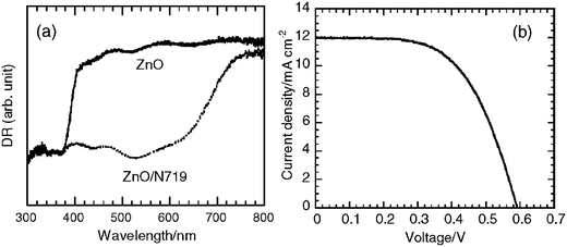 | ||
| Fig. 2 (a) Diffuse reflectance spectra of the ZnO film and the ZnO/N719 electrode. (b) The I–V curve of the cell using the ZnO/N719 electrode. | ||
Hereafter, we describe the optimization procedure to obtain high-current ZnO DSCs. First, the film thickness was changed by repeating the coating/drying process of the nanocrystalline paste on the FTO substrate, using thinner plastic tapes (58 μm in thickness) for the squeegee method. A larger film thickness of 16.1 μm was then obtained with the repetition three times. As a result, the amount of loaded dye was increased to 1.29 × 10⁻⁷ mol cm−2, which led to an enhanced solar energy conversion efficiency (4.39%). We then introduced a second layer consisting of ZnO particles 600 nm in diameter on the 16.1 μm thick ZnO film by the similar squeegee printing method, expecting enhanced light harvesting capability. A total film thickness was increased to 22.8 μm. Curve 1 in Fig. 3 represents I–V characteristic of a cell using this ZnO electrode with N719. A comparison with Fig. 2b clearly indicates that the performance is enhanced, especially in Jsc (13.76 mA cm−2) (see also Table 1).
| Sample | J sc /mA cm−2 | V oc/V | ff | η (%) |
|---|---|---|---|---|
| 1 | 13.76 | 0.574 | 0.573 | 4.53 |
| 2 | 16.31 | 0.613 | 0.522 | 5.22 |
| 3 | 18.11 | 0.621 | 0.585 | 6.58 |
 | ||
| Fig. 3 I–V curves of the cells fabricated through three kinds of the optimization; (1) the introduction of the multilayer structure, (2) the extension of the dye-loading time and (3) the decrease in the distance between the electrodes. | ||
As we mentioned above, a simple increase of the cell efficiency is expected along extension of the dye-loading time. The 22.8 μm thick film was immersed in the N719 solution for a prolonged time of 3 h. Consequently, the dye amount was more increased (1.46 × 10⁻⁷ mol cm−2) and Jsc reached 16.31 mA cm−2 as represented by Curve 2 in Fig. 3. All of these data were collected with the cells of which the distance between the electrodes was relatively large at 120 μm. It has been reported that the Jsc value depends on the electrode distance and usually increases with decreasing distance probably due to the reduction of diffusion length and resistance of the electrolyte.13 As a final attempt in this study, the electrode distance was changed to 25 μm. All the other conditions were kept the same. A considerable enhancement of the cell performance is observed with Curve 3 in Fig. 3; namely, Jsc = 18.11 mA cm−2, Voc = 0.621 V, ff = 0.585 and η = 6.58%. This Jsc value is far beyond those reported so far with ZnO-based DSCs and is slightly higher than the TiO2-based cell (17.73 mA cm−2) showing η = 11.18 %.9
Photocurrent action spectra of the cell using the photoanode (Sample 3) are shown in Fig. 4. The maximum incident photon-to-current conversion efficiency (IPCE) reaches 80%. We verified these data by comparing them with our previous data for the ZnO/N719 cell which marked Jsc = 12.6 mA cm−2 and η = 4.1%.7 It is clearly seen that IPCE is largely improved in the present cell as much as 14–21 % in the 520–680 nm range. This fact supports the high current and efficiency of the cell observed in the I–V measurement. The improvement of IPCE in the longer wavelength region is ascribed to the introduction of the 6.7 μm thick light-scattering layer as described above. In a theoretical consideration, Jsc of the N719 sensitizer is deduced to be approximately 20 mA cm−2 if the incident light loss is 10% and IPCE is 85%.14 The theoretical energy conversion efficiency of N719 is then estimated to be around 14%. We preliminarily confirmed the presence of approximately 10% light loss due to absorption and reflection by the FTO glass substrate. Therefore the large photocurrent generation in our DSC is the result of the appropriate microstructure of the ZnO film.
 | ||
| Fig. 4 Photocurrent action spectra of the cell using the ZnO/N719 photoanode (Sample 3). Also shown are spectra of the previously reported ZnO/N719 cell with Jsc = 12.6 mA cm−2 and η = 4.1% (see details in ref. 7). | ||
It should be mentioned that the specific surface area and hence the roughness factor of our ZnO films are higher than those reported previously.4 This is one of the reasons for the improvement in the dye sensitization. Nonetheless, our values are still smaller than those of TiO2 films in the latest report.15 Furthermore, the Voc and ff values are quite low, which is supposed to result from the recombination of electrons in the ZnO conduction band and the oxidized dye or electrolyte. Because a higher Voc (0.79 V) has been reported recently in ZnO-based cells,16 further improvements of the cell performance are expected by modifying the ZnO film structure and the other cell components.
Conclusions
The ZnO films were prepared by printing the nanocrystalline pastes, followed by drying at 90 °C and heating at 450 °C. The sensitization with N719 and the optimization of the cell structure led to the high-current DSC with the short-circuit photocurrent density of 18.11 mA cm−2 and the solar energy conversion efficiency of 6.58% (AM 1.5, 100 mW cm−2).References
- B. O'Regan and M. Grätzel, Nature, 1991, 353, 737 CrossRef CAS.
- (a) T. Yoshida, K. Terada, D. Schlettwein, T. Oekermann, T. Sugiura and H. Minoura, Adv. Mater., 2000, 12, 1214 CrossRef CAS; (b) A. Kay and M. Grätzel, Chem. Mater., 2002, 14, 2930 CrossRef CAS; (c) A. K. Jana, J. Photochem. Photobiol., A, 2000, 132, 1 CrossRef CAS; (d) K. Sayama, H. Sugihara and H. Arakawa, Chem. Mater., 1998, 10, 3825 CrossRef CAS.
- (a) C. Bauer, G. Boschloo, E. Mukhtar and A. Hagfeldt, J. Phys. Chem. B, 2001, 105, 5585 CrossRef CAS; (b) R. Katoh, A. Furube, T. Yoshihara, K. Hara, G. Fujihashi, S. Takako, S. Murata, H. Arakawa and M. Tachiya, J. Phys. Chem. B, 2004, 108, 4818 CrossRef CAS.
- K. Keis, E. Magnusson, H. Lindström, S. E. Lindquist and A. Hagfeldt, Sol. Energy Mater. Sol. Cells, 2002, 73, 51 CrossRef.
- (a) E. Hosono, S. Fujihara, T. Kimura and H. Imai, J. Colloid Interface Sci., 2004, 272, 391 CrossRef CAS; (b) E. Hosono, S. Fujihara and T. Kimura, Electrochim. Acta, 2004, 49, 2287 CrossRef CAS.
- E. Hosono, S. Fujihara, I. Honma and H. Zhou, Adv. Mater., 2005, 17, 2091 CrossRef CAS.
- K. Kakiuchi, E. Hosono and S. Fujihara, J. Photochem. Photobiol., A, 2006, 179, 81 CrossRef CAS.
- K. Kakiuchi, M. Saito and S. Fujihara, Thin Solid Films, 2008, 516, 2026 CrossRef CAS.
- M. K. Nazeeruddin, F. D. Angelis, S. Fantacci, A. Selloni, G. Viscardi, P. Liska, S. Ito, B. Takeru and M. Grätzel, J. Am. Chem. Soc., 2005, 127, 16835 CrossRef CAS.
- Q. Wang, S. Ito, M. Grätzel, F. Fabregat-Santiago, I. Mora-Seró, J. Bisquert, T. Bessho and H. Imai, J. Phys. Chem. B, 2006, 110, 25210 CrossRef CAS.
- E. Hosono, S. Fujihara, T. Kimura and H. Imai, J. Sol–Gel Sci. Technol., 2004, 29, 71 CrossRef CAS.
- M. Grätzel, Inorg. Chem., 2005, 44, 6841 CrossRef.
- (a) T. Hoshikawa, M. Yamada, R. Kikuchi and K. Eguchi, J. Electrochem. Soc., 2005, 152, E68 CrossRef CAS; (b) W. J. Lee, A. Suzuki, K. Imaeda, H. Okada, A. Wakahara and A. Yoshida, Jpn. J. Appl. Phys., 2004, 43, 152 CrossRef CAS.
- Z. S. Wang, H. Kawauchi, T. Kashima and H. Arakawa, Coord. Chem. Rev., 2004, 248, 1381 CrossRef CAS.
- S. Ito, T. N. Murakami, P. Comte, P. Liska, C. Grätzel, M. K. Nazeeruddin and M. Grätzel, Thin Solid Films, 2008, 516, 4613 CrossRef CAS.
- A. S. Gonçalves, M. R. Davolos, N. Masaki, S. Yanagida, A. Morandeira, J. R. Durrant, J. N. Freitas and A. F. Nogueira, Dalton Trans., 2008, 1487 RSC.
| This journal is © The Royal Society of Chemistry 2008 |