Nanowire electrochemical sensors: can we live without labels?
First published on 7th December 2006
Introduction
Lab-on-a-chip (LOC) systems for the detection of biomolecules at very low concentrations are becoming increasingly important for applications requiring high-throughput (HT) biomolecular analyses, such as protein assays for basic molecular biology research, disease marker identification, and pharmaceutical drug screening.1 Currently, fluorescence detection of target–receptor binding is the most frequently used technique, but although very sensitive, this method suffers from the need of target-labeling and possible alterations in target–receptor interactions caused by conformational changes or steric hindrance induced by the label.2 For this reason, there is considerable effort to investigate alternatives for fluorescent detection. Surface plasmon resonance (SPR) sensing3 is one promising label-free technique, but requires sophisticated optical instrumentation and is not easily made suitable for large sensor arrays. Another recently developed technique relies on electrochemical sensing, and here we will evaluate a recent variant of this, electrochemical sensing using nanowires.There has been a steep increase in reports of ultrasensitive sensors over the past few years based on nanoscale structures and devices such as nanowires,4–6 carbon nanotubes,7,8 nanoparticles,9–12 and nanocantilever beams.13,14 One-dimensional (1D) structures such as nanowires (NWs) and carbon nanotubes (CTs) are particularly compelling due to their potential for biosensing applications and suitability for large-scale high-density integration.15 This intense interest is demonstrated by the recent increase in scientific publications; for example, a recent scientific journal is devoted entirely to NWs.16 NW devices are advantageous compared to CT devices because NW devices can be fabricated from materials, such as Si, with a vast existing knowledge base of material properties, mature fabrication technologies and techniques for surface passivation and modification. Si-NW sensors have recently attracted a large amount of attention due largely to the reported high label-free detection sensitivities of biomolecules in aqueous phase and claims of ultimately detecting single molecules electrically in real-time. In this mini-review we will focus on the use of silicon nanowire (Si-NW) structures as electrochemical sensors and their application to biosensing.
Si-NW physics and label-free biomolecular detection
Si-NW sensors operated as field-effect transistors (FET) are currently the most commonly used Si-NW sensor structures. In comparison with conventional FET-based sensors, such as the ion sensitive field effect transistor (ISFET), their mode of operation is simple because they do not require the formation of a conducting channel. Because of their small size, small variations in space charge inside the Si-NW induced by binding of biomolecules is translated into measurable changes in the Si-NW conductance. In conventional FETs, typically a PNP junction is needed to isolate the bulk silicon conduction from the channel conduction. Fig. 1 shows a schematic diagram of a typical Si-NW sensor structure. The enhanced surface sensing phenomenon is due to the extremely small cross-sectional area of the Si-NW. Therefore, charge accumulation or depletion near the Si-NW surface, caused by changes in surface potential, or surface charge, results in a change in the space charge region (SCR) that is a significant portion of the Si-NW cross-sectional area.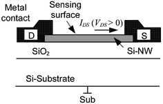 | ||
| Fig. 1 Si-NW device cross-section (not to scale). Drain (D) and source (S) contacts and electrical current IDS. The Si-NW is typically 20–50 nm. | ||
Typically, the 1D structures have diameters in the 20–50 nm range. Scaling Si-NWs widths from 200 nm down to 50 nm resulted in an estimated 20× increase in sensitivity to surface potential changes.17 Although scaling to smaller dimensions is predicted to improve surface charge sensitivity, the 1/f noise of Si-NWs has been shown to increase as the NW cross-sectional area decreases18 which may ultimately limit the Si-NW size for sensing applications.
The operation of the Si-NW FET sensors use a fixed bias current IDS by setting a voltage VDS across the drain (D) and source (S) contacts, shown in Fig. 1. The metal contacts ideally form ohmic contacts to the Si-NW. The substrate contact (Sub) should also be connected to an appropriate voltage level. In some cases the device sensitivity can be tuned with the substrate contact (also called the back gate). For a p-type Si-NW, positive charge density on the sensing surface induces electron charge carriers near the Si-NW sensing surface thus depleting hole charge carriers, or increasing the SCR, and reducing current IDS for a fixed VDS. Conversely, a negative charge at the surface induces hole accumulation, or reduction of the space charge, thus increasing IDS. Fig. 2 shows qualitative band-bending diagrams for different operation regions of a p-type Si-NW FET. In this case Fig. 2(a) shows an initial depletion of holes in the Si–NW due to positive trapped charge at the SiO2/Si-NW interface, represented as a surface potential φs. These interface charges, typically positive, can be minimized with advanced fabrication techniques.19Fig. 2(b) and (c) show band-bending diagrams of an oxidized p-type Si-NW for positive and negative charges at the oxide surface, respectively. The modulation of the initial SCR, due to changes in the surface charge density, can be significant for the 1D nanostructures and can result in measurable modulation of the device conductance, or current IDS, for a fixed VDS. Since the NW surface is ultrasensitive to surface charge, then it is also sensitive to pH changes and ionic screening of the attached molecules.
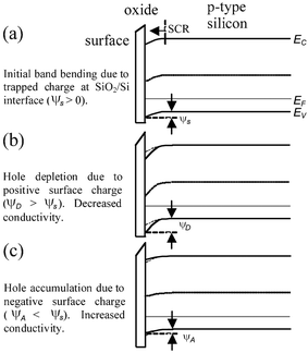 | ||
| Fig. 2 Qualitative band-bending diagrams for oxidized p-type Si-NW surfaces. (a) Initial bending due to SiO2/Si charge resulting in hole depletion, (b) negative surface charge at oxide surface resulting in increased hole depletion (decreased conductance), (c) positive surface charges leads to hole accumulation (increased conductance). | ||
The Si-NW sensor operation is next described quantitatively with molecular binding measurements presented in recent literature. Cui et al.4 demonstrated a series of experiments on synthesized p-type oxidized Si-NWs with length 2 µm and 20 nm diameter. In the first set of experiments, the oxidized Si-NW surface was covalently functionalized with a self-assembled monolayer (SAM) 3-aminopropyl-triethoxysilane (APTES), shown in Fig. 3. The APTES layer has mixed amine NH2 and hydroxyl OH, or silanol SiOH, terminal groups that have different dissociation values, which therefore respond differently to the solvent pH level. Both modified and unmodified responses were shown at pH levels from 2 to 10. Fig. 4(a) shows the conductance response versus solvent pH for a surface-modified NW. At low pH, the amine group is protonated giving NH3+ resulting in depletion of holes at the Si-NW/SiO2 interface and thus a reduction in electrical conductance, shown qualitatively in the band diagram in Fig. 2(b). At high pH levels, the silanol is deprotonated to SiO−, resulting in hole accumulation, thus increasing the conductance, shown in the Fig. 2(c) band diagram. The reported pH-conductance behavior of the modified Si-NWs is linear with slope 100 ± 20 nS per pH. The unmodified NW conductance versus pH was measured and the response is shown in Fig. 4(b). Clearly the unmodified Si-NW SiO2 surface is dependent on the solvent pH indicating careful control of the surface potential is necessary requiring reference electrodes for complex solution mixtures.
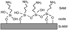 | ||
| Fig. 3 3-Aminopropyltriethoxysilane (APTES) self-assembled monolayer on oxidized Si-surfaces with amine NH2 and hydroxyl OH terminal groups. Reprinted with permission from ref. 20 (Langmuir, 2000, 16, 2651–2657). Copyright 2000 American Chemical Society. | ||
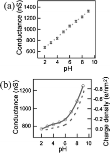 | ||
| Fig. 4 Si-NW conductance versus pH for (a) modified oxide surfaces and (b) unmodified oxide surfaces. (a) Reprinted with permission from ref. 4 (Science, 2001, 293, 1289–1291). Copyright 2001 AAAS. (b) Reprinted with permission from ref. 51 (J. Phys. Chem., 1957, 61, 1166–1169). Copyright 1957 American Chemical Society. | ||
In our view, however, it would be desirable to describe Si-NW operation in terms of the so-called Site Binding Model,21 that has been used for over three decades to describe the operation of pH-ISFETs and chemical modifications thereof.22–24 The essential difference between operating the ISFET in a constant current feedback mode as opposed to the conductance sensing that is done typically with Si-NW is that in the ISFET case the output signal directly reflects the change in the surface potential, and is not a function of the device geometry. Another major difference with conventional use of ISFETs is that these were supposed to be used as separate sensors instead of being used in a dynamic mode, as is the case with most Si-NWs.
Fabrication techniques
The refinement and invention of new microfabrication techniques combined with the rapid development of new nanofabrication techniques are paving the way to the construction of functional nanoscale (∼1–100 nm) structures and devices with unprecedented precision.There are two broad classifications for NW fabrication: top down and bottom-up fabrication technologies. Top-down fabrication technology, the standard technique for semiconductor manufacturing, has been used to realize NWs from Si,17,25 Au,26,27 and Ag,26 as well as many others, and is based on standard microfabrication methods consisting of deposition, etching and ion-beam milling on planar substrates. Patterning is usually done using UV-photolithography and typically combined with advanced nanolithography techniques such as electron beam lithography (EBL) or focused-ion-beam (FIB) techniques to realize feature sizes down to 10 nm28 and ultimately down to 5–7 nm with refinements to fabrication techniques.29 The main drawback to EBL is that it is slow, and, in general, not amenable to large scale manufacturing. Replication top-down fabrication techniques such as nanoimprint lithography (NIL)30 combines the resolution of EBL with large area. High-density Si-NW arrays have recently been reported with 15 nm wide Si nanowires at a 34 nm pitch using a superlattice nanowire pattern transfer technique,31 shown in Fig. 5. Doping of the top-down fabricated Si-NWs can be achieved through ion-implantation of the desired dopant species17 or using spin-on-dopants for NW widths less than 50 nm and lengths of 10 µm due to processing induced defects.15
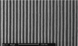 | ||
| Fig. 5 SEM of Si nanowire (15 nm wide and 34 nm pitch) mold used for nanoimprinting. Reprinted with permission from ref. 31 (Nano Lett., 2006, 6, 351–354). Copyright 2006 American Chemical Society. | ||
The bottom-up fabrication approach attempts to assemble the necessary device elements from the atomic level. A large number of NW materials, ranging from common semiconductor materials such as Si,32–34 Ge,33,35 ZnO,36,37 and SnO238,39 have been reported. These and many more material systems have been successfully synthesized into nanostructures over the last decade.40,41 A key process constraint in the synthesis of 1D nanostructure formation from a bottom-up perspective is crystallization. The evolution of a solid phase involves two fundamental steps: nucleation and growth. With sufficiently high concentrations of the atomic building blocks, small aggregate clusters are formed through homogenous nucleation and combined with a continuous supply of atomic components, the nucleation clusters serve as seeds for further growth, thus forming larger structures.40 The vapor–liquid–solid (VLS) growth method is commonly used for generating single crystal structures in large quantities. The growth process is divided into two main steps, first, the formation of a metal droplet, typically Au, that roughly defines the diameter of the wire, and second, the alloying, nucleation and growth of the wire. The growth process typically occurs in the temperature range 300–1100 °C, determined by the catalyst and the target material, with a Si-containing precursor gas. Gas mixtures containing dopants, such as B or P, can also be introduced to the precursor gas mixture resulting in in-situ p-type or n-type Si-NWs, respectively.42 The diameter of the Si-NWs is controlled by the size of the catalyst and the furnace conditions.43Fig. 6 shows high-resolution transmission electron microscopy images of VLS grown Si-NWs illustrating the crystalline structure.34 Disadvantages in bottom-up manufactured NWs include lack of controlled growth into high density arrays is not straightforward as they typically require transfer and assembly of devices on separate substrates, in addition to challenges in the formation of ohmic contacts.
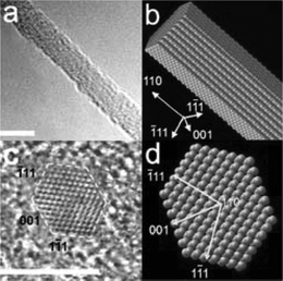 | ||
| Fig. 6 (a) 3.8 nm Si-NWs grown along the <110> direction, (c) cross-sectional image, and equilibrium shapes for (b) NW and the (d) NW cross-sections predicted by Wulff construction. Scale bar 5 nm. Reprinted with permission from ref. 34 (Nano Lett., 2004, 4, 433–436). Copyright 2004 American Chemical Society. | ||
Applications
As medical diagnostic techniques continue to progress and move towards highly specific therapies based on molecular markers, high-throughput sensors and systems for the ultrasensitive detection of biomolecular interactions are in high demand. For example, early disease detection is particularly important in the case of cancer therapies because early stages of the disease are typically treated with the greatest probability of success.44 The unique sensing properties of these nanoscale sensors have recently been demonstrated through the real-time, label-free detection of biomolecular binding to functionalized surfaces of oxidized Si-NWs.Protein detection has been demonstrated on modified oxide Si-NW surfaces for a few key disease markers. Cui et al.4 reported the detection of biotin–streptavidin on oxidized Si-NW surfaces. The oxide surfaces were modified with biotin. Binding of streptavidin to the biotin in a phosphate buffer with pH 9 was demonstrated. The addition of 250 nM of streptavidin resulted in a conductance increase of ∼50 nS, region 2 in Fig. 7. The pH change due to the streptavidin was not reported, but following the measurement of biotin–streptavidin binding pure buffer solution of pH 9 was reintroduced without change to the increased conductance measurement, shown in region 3 of Fig. 7. A sensitivity limit of at least 10 pM has been reported.
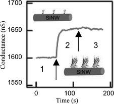 | ||
| Fig. 7 Real-time detection of biotin–streptavidin binding to an oxidized p-type Si-NW. Reprinted with permission from ref. 4 (Science, 2001, 293, 1289–1291). Copyright 2001 AAAS. | ||
An important aspect in using Si-NW sensors for protein detection is the ability to measure real-time interactions of multiple protein biomarkers simultaneously using large arrays of sensing elements. Zheng et al.45 used multiplexed electrically addressable Si-NWs sensor arrays to detect prostate specific antigen (PSA) of at least 0.9 pg ml−1 in undiluted serum samples. The plasma cleaned Si-NW oxide layer was covalently modified with an aldehyde propyl trimethoxysilane (APTMS) and the terminal aldehyde groups were later functionalized with a mAb receptor protein. Further experiments were reported where a single PSA biomarker was detected by modifying the Si-NW devices with a monoclonal antibody PSA-Ab1. The measured data indicate the direct detection of PSA for concentrations near 2 fM. In another report, Patolsky et al.46 describe the real-time label-free detection of a single virus molecule on antibody-modified p-type Si-NWs. The Si-NWs were first modified with 3-(trimethoxysilyl)propyl aldehyde and then linked with anti-hemagglutinin and mAb receptor for the influenza-A virus. Fig. 8 demonstrates a single influenza-A virus-binding event using the real-time electrical measurement corroborated with optical measurements of a fluorescently labeled (DiIC18 dye) virus target. The influenza-A virus solution was introduced to the solvent at point 1, and the solvent was changed to pure buffer between points 4 and 5. The fluorescent images correspond to points 1–8 in the conductance data. Points 2 and 4 show conductance decreases indicating positive surface charge increases for a single and two virus particles, respectively. Points 6 and 8 indicate virus unbinding from the surface.
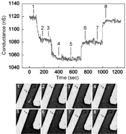 | ||
| Fig. 8 Simultaneous conductance and optical versus time data recorded from a single nanowire device with a high density of anti-influenza type-A antibody. Reproduced from ref. 46 (Proc. Natl. Acad. Sci., U. S. A., 2004, 101, 14017). Copyright © 2004 The National Academy of Sciences of the United States of America, all rights reserved. | ||
Another important application of real-time label-free biosensors is for the detection of DNA hybridization. Current methods have mainly focused on optical detection using fluorescently labeled oligonucleotides. Label-free electronic methods promise to offer sensitivity, selectivity, and low cost detection of DNA hybridization. The hybridization of DNA complexes on modified Si–NWs surfaces has been measured using label-free Si-NW sensors. In a report by Hahm et al.,47 the label-free electrical detection of peptide nucleic acid (PNA)-DNA hybridization with a detection limit as low as 10 fM was reported. The oxide surfaces of the Si-NW devices were modified with an avidin protein linked directly to the oxide and later linked with a biotinylated PNA probe molecule designed to recognize wild type versus the ΔF508 mutation site in the cystic fibrosis transmembrane receptor gene. In an article appearing one month later, Li et al.,48 reported the detection of ssDNA target molecules using 12-mer oligonucleotide probe molecules attached to a 20 µm long top-down fabricated p-type Si–NW device with 50 × 50 nm2 cross-sectional area. The oligonucleotides were attached to the oxide surfaces in two steps: first, covalent attachment of 3-mercapto-propyltrimethoxysilane (MPTMS) SAM to the oxide surface, and second, covalent linking of the 5′-end of the oligonucleotide to the SAM attached to the oxide surface. Complementary DNA was introduced in deionized water to avoid ion-screening effects. DNA hybridization was measured with a detection limit of 25 pM. In a later article Li et al.17 replaced the oligonucleotide probes with PNA probe molecules and reported an increased sensitivity of 10 pM, still three orders of magnitude larger than that reported earlier.47 In both reports the pH of the solvent was not mentioned and the conductance change is attributed entirely to the hybridization of the target DNA to the probe molecules. Fig. 9 shows an example of the measured conductance changes for Si–NWs of different dimensions and different DNA sample concentrations.
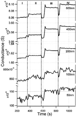 | ||
| Fig. 9 Time response of DNA hybridization on five sensors with different dimensions at 4 stages of the experiment. I: DI water; II: 10 nM non-complementary DNA solution; III: 10 pM complementary DNA solution; IV: 100 pM complementary DNA solution. Reproduced from ref. 17 (Li et al., Appl. Phys. A: Mater. Sci. Process., 2005, 80, 1257–1263) with kind permission of Springer Science and Business Media. | ||
As mentioned previously, the ability to detect thousands of protein interactions simultaneously with label-free, real-time electrical techniques will require multiplexing the dense arrays of sensors each one electrically addressable to micron dimensions for conventional electrical connection to the signal processing and data recording instruments. Si–NW density is limited to the electrical addressing of the sensors. Demultiplexing architectures based on binary input trees have been proposed.15,49,50
Summary
Based on the impressive sensing capabilities reported so far, the continued development of NW sensors may significantly impact many fields that can benefit from label-free real-time sensor arrays, such as genomics, proteomics, drug discovery, and medical diagnostics. Although significant progress has been made in demonstrating the capability of detecting molecular binding to modified Si–NW surfaces, more work is necessary to quantitatively describe the physical and chemical mechanisms during the binding and detection process. We believe that use of the Site Binding Model to describe the surface potential variations as function of concentration of binding species is essential for proper understanding of Si-NW biosensor functionality. Additionally, the use of a reference electrode will provide a way to better control the surface potential and thus the sensitivity of the devices.Edwin T. Carlen
e.t.carlen@ewi.utwente.nl
Albert van den Berg
a.vandenberg@ewi.utwente.nl
BIOS/Lab-on-a-Chip group, MESA+ Research Institute, University of Twente, The Netherlands
References
- P. Bertone and M. Snyder, FEBS J., 2005, 272, 5400 Search PubMed.
- N. Ramachandran, D. N. Larson, P. R. H. Stark, E. Hainsworth and J. LaBaer, FEBS J., 2005, 272, 5412 Search PubMed.
- J. Homola, S. S. Yee and G. Gauglitz, Sens. Actuators, B, 1999, 54, 3 CrossRef.
- Y. Cui, Q. Q. Wei, H. K. Park and C. M. Lieber, Science, 2001, 293, 1289 CrossRef CAS.
- X. T. Zhou, J. Q. Hu, C. P. Li, D. D. D. Ma, C. S. Lee and S. T. Lee, Chem. Phys. Lett., 2003, 369, 220 CrossRef CAS.
- Z. Li, Y. Chen, X. Li, T. I. Kamins, K. Nauka and R. S. Williams, Nano Lett., 2004, 4, 245 CrossRef CAS.
- S. J. Tans, M. H. Devoret, H. J. Dai, A. Thess, R. E. Smalley, L. J. Geerligs and C. Dekker, Nature, 1997, 386, 474 CrossRef CAS.
- P. Avouris, J. Appenzeller, R. Martel and S. J. Wind, Pr. Inst. Electr. Elect., 2003, 91, 1772 Search PubMed.
- L. Brus, Appl. Phys. A: Mater. Sci. Process., 1991, 53, 465 CrossRef.
- A. P. Alivisatos, Science, 1996, 271, 933 CrossRef CAS.
- S. A. Empedocles, D. J. Norris and M. G. Bawendi, Phys. Rev. Lett., 1996, 77, 3873 CrossRef CAS.
- A. J. Haes and R. P. Van Duyne, J. Am. Chem. Soc., 2002, 124, 10596 CrossRef CAS.
- J. Fritz, M. K. Baller, H. P. Lang, H. Rothuizen, P. Vettiger, E. Meyer, H.-J. Güntherodt, Ch. Gerber and J. K. Gimzewski, Science, 2000, 288, 316 CrossRef CAS.
- H. G. Craighead, Science, 2000, 290, 1532 CrossRef CAS.
- R. Beckman, E. Johnston-Halperin, Y. Luo, J. E. Green and J. R. Heath, Science, 2005, 310, 465 CrossRef CAS.
- J. E. Fischer, Appl. Phys. A: Mater. Sci. Process., 2006, 85, 209 CrossRef.
- Z. Li, B. Rajendran, T. I. Kamins, X. Li, Y. Chen and R. S. Williams, Appl. Phys. A: Mater. Sci. Process., 2005, 80, 1257 CrossRef CAS.
- S. Reza, G. Bosman, M. Saif Islam, T. I. Kamins, S. Sharma and R. S. Williams, IEEE Trans. Nanotechnol., 2006, 5, 523 CrossRef.
- S. M. Sze, Physics of Semiconductor Devices, 2nd edn, John Wiley & Sons, Inc., 1981 Search PubMed.
- P. A. Heiney, K. Grüneberg, J. Fang, C. Dulcey and R. Shashidhar, Langmuir, 2000, 16, 2651 CrossRef CAS.
- D. E. Yates, S. Levine and T. W. Healy, J. Chem. Soc., Faraday Trans. 1, 1974, 70, 1807 RSC.
- L. Bousse, N. F. DeRooij and P. Bergveld, IEEE Trans. Electron Devices, 1983, ED-30, 1263 CrossRef.
- A. van den Berg, P. Bergveld, D. N. Reinhoudt and E. J. R. Sudholter, Sens. Actuators, 1985, 8, 129 CrossRef CAS.
- R. E. G. van Hal, J. C. T. Eijkel and P. Bergveld, Sens. Actuators, B, 1995, 24–25, 201 CrossRef.
- R. A. Beckman, E. Johnston-Halperin, N. A. Melosh, Y. Luo, J. E. Green and J. R. Heath, J. Appl. Phys., 2004, 96, 5921 CrossRef CAS.
- G. Schider, J. R. Krenn, W. Gotschy, B. Lamprecht, H. Ditlbacher, A. Leitner and F. R. Aussenegg, J. Appl. Phys., 2001, 90, 3825 CrossRef CAS.
- S. Keebaugh, A. Kaan Kalkan, W. J. Nam and S. J. Fonash, Electrochem. Solid-State, 2006, 9, H88 CrossRef CAS.
- C. Vieu, F. Carcenac, A. Pepin, Y. Chen, M. Mejias, A. Lebib, L. Manin-Ferlazzo, L. Couraud and H. Launois, Appl. Surf. Sci., 2000, 164, 111 CrossRef.
- H. G. Craighead, R. E. Howard, L. D. Jackel and P. M. Mankievich, Appl. Phys. Lett., 1983, 42, 38 CrossRef CAS.
- S. Y. Chou, P. R. Krauss and P. Renstrom, Appl. Phys. Lett., 1995, 67, 3113.
- G.-Y. Jung, E. Johnston-Halperin, W. Wu, Z. Yu, S.-Y. Wang, W. M. Tong, Z. Li, J. E. Green, B. A. Sheriff, A. Bouki, Y. Bunimovich, J. R. Heath and R. S. Williams, Nano Lett., 2006, 6, 351 CrossRef CAS.
- R. S. Wagner and W. C. Ellis, Appl. Phys. Lett., 1964, 4, 89 CAS.
- A. M. Morales and C. M. Lieber, Science, 1998, 279, 208 CrossRef CAS.
- Y. Wu, Y. Cui, L. Huynh, C. J. Barrelet, D. C. Bell and C. M. Lieber, Nano Lett., 2004, 4, 433 CrossRef CAS.
- Y. Wu and P. Yang, J. Am. Chem. Soc., 2001, 123, 3165 CrossRef CAS.
- M. H. Huang, S. Mao, H. Feick, H. Yan, Y. Wu, H. Kind, E. Weber, R. Russo and P. Yang, Science, 2001, 292, 1897 CrossRef CAS.
- Z. Fan and J. G. Lu, IEEE Trans. Nanotechnol., 2006, 5, 393 CrossRef.
- M. Law, H. Kind, B. Messer, F. Kim and P. Yang, Angew. Chem., Int. Ed., 2002, 41, 2405 CrossRef CAS.
- V. V. Sysoev, B. K. Button, K. Wepsiec, S. Dmitriev and A. Kolmakov, Nano Lett., 2006, 6, 1584 CrossRef CAS.
- Y. Xia, P. Yang, Y. Sun, Y Wu, B. Mayers, B. Gates, Y. Yin, F. Kim and H. Yan, Adv. Mater., 2003, 15, 353 CrossRef CAS.
- H. J. Fan, P. Werner and M. Zacharis, Small, 2006, 2, 700 CrossRef CAS.
- Y. Cui, X. Duan, J. Hu and C. M. Lieber, J. Phys. Chem., 2000, 104, 5213 Search PubMed.
- Y. Cui, L. J. Lauhon, M. S. Gudisen, J. Wang and C. M. Lieber, Appl. Phys. Lett., 2001, 19, 2214 CrossRef.
- M. M.-C. Cheng, G. Cuda, Y. L. Bunimovich, M. Gaspari, J. R. Heath, H. D. Hill, C. A. Mirkin, A. J. Nijdam, R. Terracciano, T. Thundat and M. Ferrari, Curr. Opin. Chem. Biol., 2006, 10, 11 CrossRef CAS.
- G. Zheng, F. Patolsky, Y. Cui, W. U. Wang and C. M. Lieber, Nat. Biotechnol., 2005, 23, 1294 CrossRef CAS.
- F. Patolsky, G. Zheng, O. Hayden, M. Lakadamyali, X. Zhuang and C. M. Lieber, Proc. Natl. Acad. Sci. U. S. A., 2004, 101, 14017 CrossRef CAS.
- J. Hahm and C. M. Lieber, Nano Lett., 2004, 4, 51 CrossRef CAS.
- Z. Li, Y. Chen, X. Li, T. I. Kamins, K. Nauka and R. S. Williams, Nano Lett., 2004, 4, 245 CrossRef CAS.
- P. J. Kuekes and R. S. Williams, US Patent, 2001, Search PubMed6
![[thin space (1/6-em)]](https://www.rsc.org/images/entities/char_2009.gif) 256767.
256767. - A. Dehon, P. Lincoln and J. Savage, IEEE Trans. Nanotechnol., 2003, 2, 165 CrossRef.
- G. H. Bolt, J. Phys. Chem., 1957, 61, 1166 CrossRef CAS.
| This journal is © The Royal Society of Chemistry 2007 |