DOI:
10.1039/B614121H
(Invited Article)
Phys. Chem. Chem. Phys., 2007,
9, 31-48
Received
28th September 2006
, Accepted 19th October 2006
First published on 22nd November 2006
Abstract
The atomic structure of a carbon nanotube can be defined by the chiral indices, (n,m), that specify its perimeter vector (chiral vector), with which the diameter and helicity are also determined. The fine electron beam available in a modern Transmission Electron Microscope (TEM) offers a unique and powerful probe to reveal the atomic structure of individual nanotubes. This article covers two aspects related to the use of the electron probe in the TEM for the study of carbon nanotubes: (i) to express the electron diffraction intensity distribution in the electron diffraction patterns of carbon nanotubes and (ii) to obtain the chiral indices (n,m) of carbon nanotubes from their electron diffraction patterns. For a nanotube of given chiral indices (n,m), the electron scattering amplitude from the carbon nanotube can be expressed analytically in closed form using the helical diffraction theory, from which its electron diffraction pattern can be calculated and understood. The reverse problem, i.e., assignment of the chiral indices (n,m) of a carbon nanotube from its electron diffraction pattern, is approached from the relationship between the electron diffraction intensity distribution and the chiral indices (n,m). The first method is to obtain indiscriminately the chiral indices (n,m) by reading directly the intensity distribution on the three principal layer lines, l1, l2, and l3, which have intensities proportional to the square of the Bessel functions of orders m, n, and n + m: Il1
∝ |Jm (πdR)|2, Il2
∝ |Jn (πdR)|2, and Il3
∝ |Jn+m (πdR)|2. The second method is to obtain and use the ratio of the indices n/m = (2D1
−
D2)/(2D2
−
D1) in which D1 and D2 are the spacings of principal layer lines l1 and l2, respectively. Examples of using these methods are also illustrated in the determination of chiral indices of isolated individual single-walled carbon nanotubes, a bundle of single-walled carbon nanotubes, and multi-walled carbon nanotubes.
Introduction
Diamond and graphite have long been regarded as the only allotropes of crystalline carbon and their atomic structures were determined soon after the X-ray diffraction method was developed in the early 1910’s.1–3 The discovery of fullerenes and the subsequent success in their large scale synthesis prompted renewed searches of unknown structures of carbon at the nanometer scale.4,5 Carbon nanotubes were first identified by Iijima in 19916 in the cathodic deposits produced by dc arc-discharge of two graphite electrodes in an apparatus developed to produce fine particles and fullerenes.7 The ultimate form of carbon nanotubes is single-walled carbon nanotubes,8,9 which can be constructed schematically by rolling up a rectangular cut of graphene about a chosen axis to form a seamless cylinder of diameter on the nanometer scale.
The atomic structure of a single-walled carbon nanotube is well described by its chiral indices (n,m) that specify the perimeter of the carbon nanotube on the graphene net. The determination of the chiral indices has been a challenge to researchers ever since carbon nanotubes were discovered. Transmission Electron Microscopy (TEM) has been the most powerful and most popular technique in characterizing the morphology and structure of carbon nanotubes. In addition to the TEM method, other analytical techniques, especially Raman spectroscopy,10,11 optical absorption spectroscopy,12,13 and scanning tunneling microscopy14–18 have also been used extensively in attempt to elucidate the atomic structure and to obtain the chiral indices of carbon nanotubes. However, due to various limitations, there are still formidable difficulties to determine the atomic structure of carbon nanotubes accurately with these techniques.
Electron diffraction was the first technique employed to identify the helical nature in the structure of carbon nanotubes6 and it has continued to play a vital role in the structural studies of carbon nanotubes. Based on the helical theory developed for the study of α-helix and the helical DNA molecules,19–25 the kinematical diffraction theory for the scattering of electrons or X-rays from carbon nanotubes was formulated by Qin in 199426 and subsequently by Lucas et al. in 1996.27–29 In addition, electron diffraction from carbon nanotubes was also discussed extensively using geometric illustrations.30–35 On the other hand, electron diffraction has also been explored for the possibility of solving the atomic structure of carbon nanotubes, in particular, to obtain the helicity of carbon nanotubes over the past fifteen years.36–46 Two approaches have been developed: one using a correction factor to obtain the chiral angle from the electron diffraction pattern,39 and the other using the ratio of the layer lines measured in the electron diffraction patterns.45 The atomic structure of a double-walled carbon nanotube was also obtained by an electron crystallographic method using phase retrieval.47 Most recently, a one-step direct method has been developed48 and has been applied to determine the atomic structure of a large number of carbon nanotubes, both single- and multi-walled.49–51 Electron diffraction is by far the most powerful technique for studying the atomic structure, including the handedness, of carbon nanotubes with high accuracy, as can be seen in the literature.52–85
The solid state physics convention is used in this article to describe the graphene lattice structure, where the basis vectors of the graphene net, ![[a with combining right harpoon above (vector)]](https://www.rsc.org/images/entities/i_char_0061_20d1.gif) 1 and 2 (a1 = a2 = a0 = 0.246 nm), are separated with an inter-angle of 60°, as shown schematically in Fig. 1(a) in radial projection. On the graphene net, the chiral indices (n,m) specify the perimeter of the carbon nanotube, as shown schematically in Fig. 1(a) for the chiral vector (7,1). For a carbon nanotube of given chiral indices (n,m), its perimeter vector is
1 and 2 (a1 = a2 = a0 = 0.246 nm), are separated with an inter-angle of 60°, as shown schematically in Fig. 1(a) in radial projection. On the graphene net, the chiral indices (n,m) specify the perimeter of the carbon nanotube, as shown schematically in Fig. 1(a) for the chiral vector (7,1). For a carbon nanotube of given chiral indices (n,m), its perimeter vector is| |  | (1) |
which has a magnitude A = a0(n2 + m2 + nm)1/2. The diameter, d, of the carbon nanotube is | |  | (2) |
and the helicity, α, defined as the angle between the perimeter vector, ![[A with combining right harpoon above (vector)]](https://www.rsc.org/images/entities/i_char_0041_20d1.gif) = (n,m), and the basis vector, 1, illustrated in Fig. 1(a), is
= (n,m), and the basis vector, 1, illustrated in Fig. 1(a), is| |  | (3) |
Once the chiral indices (n,m) of a carbon nanotube are assigned, the tubule axis, (nc,mc), perpendicular to the chiral vector, , can be calculated by applying the orthogonality relationship between the tubule perimeter and the tubule axis, which yields| |  | (4) |
The indices of the tubule axis (nc,mc) should be chosen as the pair which has no common factors other than 1. Denoting M as the greatest common integer divisor of integers (2n + m) and (n + 2m), the axial lattice vector (nc,mc) can then be expressed as| |  | (5) |
and the axial periodicity, c, of carbon nanotube (n,m) can also be obtained86| |  | (6) |
When a rectangle with sides A and c is cut out of the graphene and is then rolled up about the tubule axis, c, perpendicular to the perimeter, A, a cylindrical nanotube (7,1) is formed as shown in Fig. 1(b).
 |
| | Fig. 1 (a) Schematic structure of graphene with basis vectors 1 and 2. The shadowed rectangle is the radial projection of carbon nanotube (7,1) with perimeter and helical angle α. (b) Single-walled carbon nanotube (7,1) is formed from the cut by rolling it up about axis ![[c with combining right harpoon above (vector)]](https://www.rsc.org/images/entities/i_char_0063_20d1.gif) perpendicular to the perimeter vector . perpendicular to the perimeter vector . | |
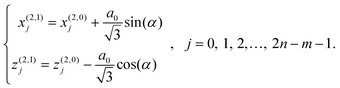
The atomic positions of a single-walled carbon nanotube can be conveniently expressed by the Cartesian coordinates (xj, zj) in the radial projection, where the nanotube is projected onto a rectangle with sides A and c as described above. In fact, the atomic structure of the carbon nanotube can be described by pairs of parallel atomic helices. There are three equivalent molecular helices in a single-walled carbon nanotube. They are parallel to the directions of the basis vectors 1, 2, and 3 = 2
−
1, respectively. The three primary helices are indicated on the graphene net as shown in Fig. 2(a). Each helix consists of a pair of atomic helices, displaced by a translational vector. Within a repetition unit in the axial direction, there are m helix pairs parallel to 1, n helix pairs parallel to 2, and n + m helix pairs parallel to 3 = 2
−
1. With respect to a chosen carbon atom located at the origin, there are n + m atoms on the primary helix parallel to 1 and their coordinates are (c.f. Fig. 2(b))
| |  | (7) |
and the atoms on the secondary helix are at
| |  | (8) |
The atomic structure of the
carbon nanotube can then be described by the
m such helix pairs by translating the primary helix pair by multiples of the basis vector
3:
| |  | (9) |
Similarly, the atomic positions on the primary helix parallel to
2 (left handed—the
axis is inverted in calculating the atomic coordinates) are
| |  | (10) |
and the atoms on the secondary helix are at
| |  | (11) |
The atomic structure of the
carbon nanotube can be expressed by the
n helix pairs generated by translating the primary helix pair by multiples of
1| |  | (12) |
The atomic positions on the primary helix parallel to
3 =
2
−
1 are
| |  | (13) |
and the secondary helix is
| |  | (14) |
The atomic structure of the
carbon nanotube can be expressed by the
n +
m helix pairs generated by translating the primary helix pair by multiples of
1| |  | (15) |
Due to the hexagonal rotational symmetry of the
graphene lattice, the non-degenerate range for helicity,
α, is 60°, which can be confined to the range of [0°,60°]. The values in [0°,30°] can be assigned to the right-handed tubules, while the values [30°,60°] are for the left-handed tubules. Among the three helices, two have the same handedness and the third has opposite handedness. Therefore, though the structure of
carbon nanotubes is enantiomorphic, the choice of absolute handedness is arbitrary.
 |
| | Fig. 2 (a) Schematic illustrating the principal helices that are parallel to the basis vectors 1 (solid), 2 (dashed) and 3 = 2
−
1 (dotted). (b) Definition of the chiral vector A, axial direction C, and the basis vectors 1, 2 and 3 = 2
−
1. | |
When the handedness of a tubule is ignored, the helical angle can be limited to [0°,30°]. Within this range, the chiral indices (n,m) are limited to values n
≥
m
≥ 0.
The rotational symmetry of a nanotube can be recognized by examining its chiral indices, (n,m). A carbon nanotube of indices (n,m) has N-fold rotational symmetry, with N being the greatest common divisor of n and m. When m = 0, the carbon nanotube possesses n-fold rotational symmetry, and it does not have a two-fold rotational symmetry when n is an odd number. On the other hand, when a two-fold axis is present, the carbon nanotube is also centrosymmetric.
There are two special non-helical structures that deserve special attention. One is the so-called zigzag structure, which has chiral indices of the form (n,0) with a helical angle α = 0°, as shown in Fig. 3(a); the other is the armchair structure, which has indices of (n,n) with a helical angle α = 30°, shown in Fig. 3(b). In the zigzag structure, the tubule axis is (nc,mc) = (−1, 2) and in the armchair structure it is (nc,mc) = (−1, 1).
 |
| | Fig. 3 (a) Carbon nanotube (18,0) (d = 1.409 nm and α = 0°) of zigzag structure; (b) nanotube (10,10) (d = 1.36 nm and α = 30°) of armchair structure. | |
Diffraction from a continuous helix
The electron scattering amplitude can be expressed by the structure factor| |  | (16) |
where V(![[r with combining right harpoon above (vector)]](https://www.rsc.org/images/entities/i_char_0072_20d1.gif) ) is the modified scattering potential proportional to the Coulombic potential of the scattering object,
) is the modified scattering potential proportional to the Coulombic potential of the scattering object, ![[q with combining right harpoon above (vector)]](https://www.rsc.org/images/entities/i_char_0071_20d1.gif) is the scattering vector (q = 2sin(Θ/2)/λ) with Θ and λ being the scattering angle and electron wavelength, respectively. The physically measurable diffraction intensity I() in the reciprocal space is I() = |F()|2. For the general case of kinematical diffraction, where the Friedel's law holds, the diffraction intensity distribution is always centrosymmetric regardless of the symmetry of the scattering potential, i.e., I(−) = I(). For a cylindrical object like a nanotube, it is more convenient to express the scattering amplitude in the polar coordinates (R, Φ, l) (cf. Appendix)
is the scattering vector (q = 2sin(Θ/2)/λ) with Θ and λ being the scattering angle and electron wavelength, respectively. The physically measurable diffraction intensity I() in the reciprocal space is I() = |F()|2. For the general case of kinematical diffraction, where the Friedel's law holds, the diffraction intensity distribution is always centrosymmetric regardless of the symmetry of the scattering potential, i.e., I(−) = I(). For a cylindrical object like a nanotube, it is more convenient to express the scattering amplitude in the polar coordinates (R, Φ, l) (cf. Appendix)| |  | (17) |
where Jh(2πrR) is the Bessel function of integer order h and c is the structural periodicity of the tubular object in the direction of its unique axis (z-direction).
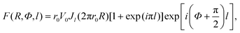
As an example to illustrate the scattering of helical structures, Fig. 4(a) shows a right-handed continuous helix of radius r0 and pitch length C. The scattering potential can be expressed by
| |  | (18) |
Using this potential, the scattering amplitude (17) becomes
| |  | (19) |
and the corresponding scattering intensity distribution is
| |  | (20) |
which is plotted in
Fig. 4(b).
 |
| | Fig. 4 (a) Schematic of a continuous helix of pitch length C. (b) Corresponding electron diffraction pattern of the continuous helix. It consists of a set of layer lines separated by 1/C and the intensity on layer line l is proportional to|Jl(X)2|. (c) Two continuous helices with a phase difference of π and (d) the Fraunhofer diffraction pattern where the layer lines of odd indices are in extinction. | |
There are two important characteristics in the Fraunhofer diffraction pattern of a helix that deserve special mention. One is that the intensity (eqn (20)) falls only on discrete lines (layer lines) indexed by integer l; the other is that the intensity on a layer line l is proportional to the square of the Bessel function of order l.
When there are two helices, shown schematically in Fig. 4(c), related by a twofold rotation axis, i.e.,
| |  | (21) |
the scattering amplitude then becomes
| |  | (22) |
and the intensity distribution is
| |  | (23) |
The layer lines of odd index
l are in extinction, as shown in
Fig. 4(d).
When there is an N-fold rotation axis, the layer lines will be in extinction except for those of indices equal to multiples of N. Correspondingly, the diffraction intensity on layer line of index l = sN is proportional to |JsN (2πr0R)|2.
For a single-walled carbon nanotube of radius r0, where the carbon atoms are located at discrete positions on a helix of radius r0, as shown schematically in Fig. 5(a), the corresponding structure factor can be expressed as (cf. Appendix)| |  | (24) |
where the summation for j is done over all atoms in a unit cell and h over all integers as allowed by the selection rule. This is a generic formula that is valid for all forms of nanotubes, elemental or composite.
 |
| | Fig. 5 (a) Schematic of a discontinuous helix where discrete groups of scatterers (atoms) are located on a helix of pitch length C. The periodicity of the structure and the separation between the neighboring molecular groups in the axial direction are given by c and Δ, respectively. (b) The corresponding Fraunhofer diffraction pattern. | |
The structure factor (eqn (24)) can also be rewritten as
| |  | (25) |
where
| | 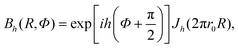 | (26) |
and
| |  | (27) |
with (
xj,
zj) being the atomic coordinates in radial projection in the horizontal and axial directions, respectively. Herewith, the diffraction effects from a cylindrical
nanotube are more clearly seen by examining the two parts in
eqn (25): (i) The structure factor in radial projection described by
Thl, which gives rise to the regular hexagonal diffraction pattern of
graphene, and (ii) the modifying function
Bh(
R,
Φ) that describes the effects of cylindrical curvature of the
nanotube. The modifying Bessel functions produce streaks perpendicular to the tubule axis and also shift the diffraction intensity peak positions in the diffraction pattern. The shifts are dependent on the order of the operating Bessel functions.
39
Selection rule for helix diffraction
When individual atoms are located on a continuous cylindrical helix, the scattering potential can be regarded as the product of the continuous helix and a set of equally spaced planes of spacing Δ, as illustrated in Fig. 5(a). The Fraunhofer diffraction from this structure can then be expressed by the convolution of the structure factor of the continuous helix and that of the equidistant planes. Since the latter is just a row of points located on the tubule axis with equal spacing 1/Δ, the final result is a set of diffraction patterns of the single continuous helix with origins located at each of the points on the tubule axis, as shown schematically in Fig. 5(b). Choosing c as the new structural periodicity along the tubule axis of a single helix and C as the pitch length of the continuous helix (c
≥
C), then the allowed reflections on layer line l should satisfy| |  | (28) |
where k is an integer. For a given layer line l, the allowed orders of Bessel functions Jh(2πr0R) are determined by combinations of h and all possible integers k that satisfy eqn (28). The selection rule (eqn (28)) can also be expressed equivalently as| |  | (29) |
where t = c/C gives the number of turns per unit periodicity in the axial direction and p = c/Δ gives the number of scattering units per complete period of the structure.
On the other hand, from the geometry in radial projection, for the atomic helices parallel to basis vector 1we have
| |  | (30) |
in terms of the chiral indices (
n,
m). The parameters
t and
p are then
| | 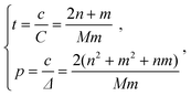 | (31) |
where
M is the greatest common divisor of (2
n +
m) and (
n + 2
m). The selection rule for
nanotube (
n,
m) can therefore also be expressed as
| |  | (32) |
When the
nanotube has rotational symmetry, the same selection rule applies if
c is defined as the periodicity related to a specific helix. The additional rotational symmetry will lead to extinction layer lines. For a
nanotube of
N-fold rotational symmetry, only
l =
sN(
l = 0, ±1, ±2,…) are allowed layer lines. Equivalently, this can be translated into additional constraints on the selection rule. If we use the structural periodicity, then the new periodicity will be shortened by
N times to become
c/
N, and the selection rule (
eqn (29))
l =
ht +
kp will limit the values of
h and
k to be multiples of
N, while
l takes all possible integers.
It should also be noted that the selection rule given by eqn (32) is derived for the specific helix parallel to basis vector 1. When the structure of a carbon nanotube is expressed by other helices (helices parallel to 2 or 3), the corresponding selection rule will appear to be different in form for each of the helices, but they are actually equivalent to each other.
To calculate the scattering amplitude for a single-walled carbon nanotube (n,m), it is more convenient to express its atomic structure by the atomic helix pairs parallel to the basis vectors 1, 2 and 3 = 1
−
2. For the m pairs of atomic helices parallel to 1 with atomic coordinates (xj(1,0), zj(1,0)) and (xj(1,1), zj(1,1)), where| |  | (33) |
and| |  | (34) |
the structure factor for the nanotube in radial projection is| |  | (35) |
By inserting| |  | (36) |
and the selection rule for the 1 helices (eqn (32)) into eqn (35), we then have| |  | (37) |
The structure factor can therefore be expressed as| |  | (38) |
where| |  | (39) |
which describes the scattering amplitude from a single helix pair parallel to 1, and| |  | (40) |
in which h, k and l are all integers that satisfy the selection rule for carbon nanotube (n,m) stipulated by eqn (32).
Visually, it is the helices that have the smallest angle with respect to the tubule axis that appear as the “helices”. For this reason, we can also choose the helices parallel to 2 in the calculation of the structure factor. By inserting the atomic positions for carbon nanotube (n,m), the scattering amplitude (eqn (24)) becomes
| |  | (41) |
where
| |  | (42) |
and
| |  | (43) |
in which
m,
n, and
l are all integers that satisfy the same selection rule (
eqn (29)) for
carbon nanotube (
n,m)
| |  | (44) |
with
M being the maximum common divisor of integers (2
n +
m) and (
n + 2
m).
Eqn (44) is equivalent to
eqn (32).
When the helices are counted in the direction of 3 = 2
−
1, then
| |  | (45) |
where
| |  | (46) |
and
| |  | (47) |
and the selection rule for the same
carbon nanotube (
n,m) appears as
| |  | (48) |
which is equivalent to
eqn (32) and (44).
The above equations are also valid for X-rays, when V() and f are replaced by the electron charge density function, ρ(), and the atomic scattering amplitude for X-rays, f(x), respectively.
An ideal multi-walled carbon nanotube consists of multiple concentric shells with inter-tubular distances similar to the inter-planar spacings of graphite (∼0.335 nm). The structure factor for a multi-walled carbon nanotube of N shells can be expressed as the coherent sum of the scattering amplitudes from all individual shells in the multi-walled carbon nanotube73| |  | (49) |
where j denotes the j-th nanotube (nj,mj) of axial periodicity cj and diameter dj, φj denotes the phase shift for the j-th shell relative to the reference shell in real space and| |  | (50) |
| |  | (51) |
in which h, k and lj are all integers governed by the selection rule for the j-th shell of the nanotube:| |  | (52) |
with Mj being the maximum common divisor of (2nj + mj) and (nj + 2mj).
The electron diffraction intensity distribution is I(R, Φ, Z) = |F(R, Φ, Z)|2.
As a special case, for electron diffraction from single-walled carbon nanotubes, the summation over j in eqn (49) disappears (N = 1) and so does the subscript j in eqn (50–52).
Principal layer lines
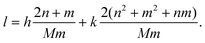
On the electron diffraction pattern of a single-walled carbon nanotube, the primary graphene reflections of Miller indices (10), (01), (11), (![[1 with combining macron]](https://www.rsc.org/images/entities/char_0031_0304.gif) 0), (0), and (), are of the strongest intensity. These reflections form three pairs of layer lines (three layer lines above the equatorial line and three below the equatorial line), labelled l1 (formed by the graphene (01) reflections), l2 (formed by the graphene (0) reflections) and l3 (formed by the graphene (11) reflections) with respective layer line spacings D1, D2, and D3 relative to the equatorial layer line. These three pairs of layer lines are referred to as the principal layer lines and are schematically illustrated in Fig. 6. It is experimentally most convenient to use these principal layer lines to characterize the carbon nanotube. Due to the very small diameter of carbon nanotubes, the diffraction peaks are elongated perpendicular to the tubule axis and only reflections close to the meridian have significant intensities. In some cases, the reflections (1) and (1) are also used, which will be referred to in this article as layer line l4 with layer line spacing D4.
0), (0), and (), are of the strongest intensity. These reflections form three pairs of layer lines (three layer lines above the equatorial line and three below the equatorial line), labelled l1 (formed by the graphene (01) reflections), l2 (formed by the graphene (0) reflections) and l3 (formed by the graphene (11) reflections) with respective layer line spacings D1, D2, and D3 relative to the equatorial layer line. These three pairs of layer lines are referred to as the principal layer lines and are schematically illustrated in Fig. 6. It is experimentally most convenient to use these principal layer lines to characterize the carbon nanotube. Due to the very small diameter of carbon nanotubes, the diffraction peaks are elongated perpendicular to the tubule axis and only reflections close to the meridian have significant intensities. In some cases, the reflections (1) and (1) are also used, which will be referred to in this article as layer line l4 with layer line spacing D4.
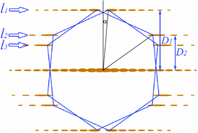 |
| | Fig. 6 Relationship between the principal graphene reflections (positioned at the six apices of the regular hexagons) and the principal layer line reflections l1, l2, and l3 of a carbon nanotube. D1 and D2 are the respective layer line spacings. Spotty graphene reflections become streaks elongated in the directions perpendicular to the tubule axis. α is the helical angle of the nanotube. | |
Direct determination of chiral Indices (n,m)
It is important to note that, on each layer line, though the scattering amplitude is expressed by a summation of all Bessel functions that are allowed by the selection rule, there is usually only one order of Bessel function that dominates the intensity distribution on a particular layer line. All the others contribute negligibly to the layer line intensity. We can deduce the above conclusion from the selection rule. Under the constraints governed by the selection rule, all the possible values of h for one chosen layer line l can be expressed as follows71| |  | (53) |
where P are positive integers that also make h an integer, and h0 defines the smallest non-negative integer for the chosen layer line l. Because (n2 + m2 + nm)/M is always an integer,79 2P(n2 + m2 + nm)/M is usually a very large number. Since the magnitude of Bessel functions decreases significantly with the increase of their orders, the diffraction intensity on a particular layer line is essentially dominated by a single Bessel function of the lowest order h0. For example, for single-walled carbon nanotube (14, 9) (d = 1.572 nm and α = 22.84°), for the principal layer line l1(l = 37), h0 = 9 and the next contributing Bessel function is h1 = 797. The magnitude of the first peak for |J9(x)|2 is more than 20 times that for |J797(x)|2. Furthermore, the first peak position of J797(x) on the layer line l1 is 75 times larger than that due to J9(x). Therefore, the diffraction intensity distribution on the layer line l = 37 for carbon nanotube (14,9) is only modulated by |J9(x)|2 within the range of collection where significant experimental data are present in the reciprocal space.
The order of the primary operating Bessel function for a given carbon nanotube (n,m) can be obtained by considering the crystallographic indices of the graphene reflections using the extended cell of the nanotube in radial projection, which is related to the index, h. In the Fraunhofer diffraction pattern of the graphene lattice, the allowed Bragg reflections are described by
| |  | (54) |
For a given
nanotube of chiral indices (
n,
m), the corresponding
nanotube reflections can also be indexed by the crystallographic indices (
h,
l) related to its radial projection net. Therefore, the selection rule should be such that the reflection
![[G with combining right harpoon above (vector)]](https://www.rsc.org/images/entities/i_char_0047_20d1.gif)
=
h* +
l![[C with combining right harpoon above (vector)]](https://www.rsc.org/images/entities/i_char_0043_20d1.gif)
* indexed using the radial projection net should fall onto the reciprocal lattice point
ḡ indexed using the
graphene lattice, where
* and
* are the basis vectors of the reciprocal lattice of the radial projection net (rectangle with sides
and
) of the
nanotube:
| |  | (55) |
The selection rule can then be written as
| |  | (56) |
or
| |  | (57) |
Multiplying both sides of
eqn (57) by
1, we obtain
| |  | (58) |
or equivalently
| |  | (59) |
Note that [
cf.
Fig. 7]
| |  | (60) |
where
γ is the angle between the basis vector
1 and the concerned
graphene reflection (
h0k0). We can then obtain the following relationship
39| |  | (61) |
As shown in
Fig. 6, the three principal layer lines,
l1,
l2 and
l3, are formed by
graphene reflections (01), (
0), and (11), respectively. When choosing the reference
graphene reflection as (01),
i.e.,
h0 = 0 and
k0 = 1, the order of the dominating Bessel function is
| |  | (62) |
and for
graphene reflection (
0)
| |  | (63) |
and for grapheme reflection (11)
| |  | (64) |
Therefore, the operating Bessel functions on the three principal layer lines,
l1,
l2, and
l3, are of orders
m, –
n, and
n +
m, respectively.
 |
| | Fig. 7 Schematic assisting the deduction of the order of the operating Bessel function on a carbon nanotube of chiral indices (n,m). a1 is the basis vector and g refers to a particular reflection of interest. A is the perimeter vector and C is the axial vector of the nanotube. α is the helical angle of the nanotube and γ is the angle between vector g and the basis vector a1. | |
The order of the dominant Bessel function on each of the principal layer lines can also be understood by the formation of the electron diffraction pattern from the three principal helices that are parallel to 1, 2, and 3 = 2
−
1, respectively. The numbers of helix pairs are m, n, and n + m, respectively. From Fig. 6, one can see that the three principal layer lines, l1, l2, and l3, correspond to these three helix pairs. Therefore, the first non-extinction reflections due to these three principal helices are expressed by the Bessel functions of order m, n, and n + m, respectively.
The same conclusion can also be reached algebraically from the selection rule.79
Therefore, the reflection intensities on the three principal layer lines, designated as layer lines l1, l2, and l3 as shown in Fig. 6, are related to the chiral indices (n,m) by
| |  | (65) |
| |  | (66) |
| |  | (67) |
and
| |  | (68) |
The order
h of Bessel function
Jh(
X) can be determined by examining the positions of its peaks, which are unique to each order of Bessel function. An efficient and convenient means to determine the order
h of Bessel function
Jh(
X) is to examine the ratio
X2/
X1 of the positions of its first two peaks located at
X1 and
X2, respectively, or any other pair of peaks unique to this Bessel function. The chiral indices (
n,m) can therefore be obtained directly by determining the order of Bessel function
Jm(
X) and
Jn(
X) with X = π
dR from the scattering intensity distribution on layer lines
l1 and
l2, whose intensities are proportional to |
Jm(π
dR)|
2 and |
Jn(π
dR)|
2, respectively. On an experimental electron diffraction pattern, the positions of the first two peaks,
R1 and
R2, can be measured and the ratio
R2/
R1 =
X2/
X1 is independent on the camera length of the electron microscope at which the electron diffraction pattern is acquired.
This method allows a rapid and accurate assignment of the chiral indices (n,m). From the electron diffraction pattern, the chiral indices m and n can be obtained by comparing the ratio R2/R1 = X2/X1 with the tabulated values given in Table 1 for Bessel functions of order up to h = 30. For Bessel functions J18(X) and J19(X), for example, the ratios of X2/X1 = R2/R1 are 1.266 and 1.256, respectively, and the difference is large enough to be identified unambiguously. Using our current method, we can obtain the peak positions with a precision of 0.3%, which allows us to assign the chiral indices unambiguously up to index 30 or nanotube diameter up to 4 nm.
Table 1 Ratio of the second and the first peak positions of Bessel functions
|
n
|
X
2/X1 |
n
|
X
2/X1 |
n
|
X
2/X1 |
| 1 |
2.892 |
11 |
1.373 |
21 |
1.239 |
| 2 |
2.197 |
12 |
1.350 |
22 |
1.232 |
| 3 |
1.907 |
13 |
1.332 |
23 |
1.226 |
| 4 |
1.751 |
14 |
1.315 |
24 |
1.218 |
| 5 |
1.639 |
15 |
1.301 |
25 |
1.211 |
| 6 |
1.565 |
16 |
1.287 |
26 |
1.206 |
| 7 |
1.507 |
17 |
1.275 |
27 |
1.201 |
| 8 |
1.465 |
18 |
1.266 |
28 |
1.196 |
| 9 |
1.428 |
19 |
1.256 |
29 |
1.192 |
| 10 |
1.398 |
20 |
1.247 |
30 |
1.188 |
Instead of using the positions of the first two peaks, other variations of this method have also been used to obtain the order of the operating Bessel functions.84
For non-helical nanotubes, i.e., zigzag and armchair nanotubes with chiral indices (n,0) and (n,n), respectively, overlap of the principal layer lines occurs. For a zigzag nanotube of indices (n,0), layer lines l2 and l3 overlap with each other and its first principal layer line (l1) has an intensity distribution proportional to |J0(πdR)|2 and the second layer line (l2) has intensity proportional to |Jn(πdR)|2. For an armchair nanotube (n,n), the first layer line l1 and the second line l2 overlap with intensities proportional to |Jn(πdR)|2 and layer line l3 falls on the equatorial line.
The major sources of error of this direct method are (i) low signal/noise ratio due to the small number of atoms in the scattering carbon nanotube and (ii) the identification of the peak positions in the intensity distribution on the principal layer lines. The signal/noise ratio can be enhanced by applying longer exposure in acquiring the experimental electron diffraction pattern.
The above conclusions are valid only for normal incidence, i.e., the incident electron beam is perpendicular to the nanotube axis. When the nanotube deviates from this normal incidence by an angle β, illustrated schematically in Fig. 8, corrections are needed for the deduction of the order of the operating Bessel function. For an incident electron beam with an inclination angle β, the structure factor becomes71
| |  | (69) |
When the tilt is taken into account, the chiral indices (
n,m) can still be derived using the direct method with a high accuracy even when the
nanotube is not oriented normal to the incident electron beam.
85
 |
| | Fig. 8 (a) Geometric relationship in electron diffraction from a carbon nanotube when it is inclined by an angle, β, to the normal to the nanotube axis. (b) Corresponding relationship in the reciprocal space where the reflection intensities due to the nanotube are a set of concentric halo rings equally spaced in the axial direction. (c) Cross-sectional view of the diffraction in the reciprocal space, where the diffraction plane intercepts the intensity halo rings. The observed separation R on an experimental diffraction pattern is smaller than the maximum value observed at β = 0°. H is the vertical height of the intercept measured from the center of the intensity rings.71 | |
Ratio of chiral indices m/n
Since the atomic structure of carbon nanotube (n,m) is periodic in the axial direction, the layer lines are sharp and the respective layer line spacings, D1, D2, and D3, can be measured accurately from the electron diffraction patterns. Although the cylindrical curvature of the nanotube causes severe distortion to the otherwise hexagonal electron diffraction pattern, the layer line spacings will not change due to the cylindrical curvature. The axial distances to the equatorial line, D1, D2, D3 and D4, of the fundamental reflections that form the principal layer lines can be calculated using the trigonometric relations illustrated schematically in Fig. 6, where α is the helical angle which is measured between the axial direction and the graphene (01) reflection in the reciprocal space| |  | (70) |
The layer line spacings are also related by| |  | (71) |
The helical angle, α, can be deduced from the ratio of the layer line spacings45| |  | (72) |
The ratio of the chiral indices m and n can be obtained by inserting eqn (3) into eqn (70)88| |  | (73) |
When the principal layer line spacings D1 and D3 are measured, for example, in terms of these two layer line spacings, the index ratio becomes| |  | (74) |
On the other hand, if the layer line spacings D3 and D4 are measured, then| |  | (75) |
In fact, when the layer line spacings D1 and D4 are accessible, the result would be most accurate by using the following calculation| |  | (76) |
eqn (73–76) offer a complimentary, and sometimes a more convenient, method to determine the chiral indices (n,m) for the following reasons:
(i) The ratio m/n is independent of the camera length at which the electron diffraction pattern is taken;
(ii) The ratio is independent of the relative orientation between the nanotube and the incident electron beam;
(iii) When the signal/noise ratio is low, this ratio can still be conveniently obtained.
The use of eqn (73–76) can result in a very high accuracy. The indeterminancy arising from the uncertainties these equations leads to only the nanotube of the smallest diameter (n0,m0). Other nanotubes meeting the same equations have chiral indices that are multiples of (n0,m0), i.e., (n,m) = (jn0, jm0), where j = 1, 2, 3, … As can be seen from the possible indices, the largest uncertainty comes from the nanotubes of chiral indices of (2m, m), where the difference in diameter between the neighboring shells is 0.207 nm. This diameter difference can be discerned from other information such as the real-space electron micrographs. To aid the use of this method, Table 2 lists all possible m/n values for chiral indices up to (30,30).
Table 2 List of m/n ratio, chiral indices (n,m), diameter (d), and helicity (α) of carbon nanotubes
|
m/n
|
n
|
m
|
d(n,m) |
α
|
m/n
|
n
|
m
|
d(n,m) |
α
|
m/n
|
n
|
m
|
d(n,m) |
α
|
m/n
|
n
|
m
|
d(n,m) |
α
|
| 0.0000 |
u
|
0 |
|
0.000 |
0.1538 |
13 |
2 |
1.105 |
7.053 |
0.2759 |
29 |
8 |
2.640 |
11.857 |
0.4000 |
5 |
2 |
0.489 |
16.102 |
| 0.0333 |
30 |
1 |
2.389 |
1.626 |
0.1538 |
26 |
4 |
2.209 |
7.053 |
0.2778 |
18 |
5 |
1.641 |
11.927 |
0.4000 |
10 |
4 |
0.978 |
16.102 |
| 0.0345 |
29 |
1 |
2.311 |
1.682 |
0.1579 |
19 |
3 |
1.618 |
7.223 |
0.2800 |
25 |
7 |
2.282 |
12.008 |
0.4000 |
15 |
6 |
1.467 |
16.102 |
| 0.0357 |
28 |
1 |
2.233 |
1.740 |
0.1600 |
25 |
4 |
2.132 |
7.311 |
0.2857 |
7 |
2 |
0.641 |
12.216 |
0.4000 |
20 |
8 |
1.956 |
16.102 |
| 0.0370 |
27 |
1 |
2.154 |
1.804 |
0.1667 |
6 |
1 |
0.513 |
7.589 |
0.2857 |
14 |
4 |
1.282 |
12.216 |
0.4000 |
25 |
10 |
2.445 |
16.102 |
| 0.0385 |
26 |
1 |
2.076 |
1.872 |
0.1667 |
12 |
2 |
1.027 |
7.589 |
0.2857 |
21 |
6 |
1.923 |
12.216 |
0.4000 |
30 |
12 |
2.934 |
16.102 |
| 0.0400 |
25 |
1 |
1.998 |
1.945 |
0.1667 |
18 |
3 |
1.540 |
7.589 |
0.2857 |
28 |
8 |
2.564 |
12.216 |
0.4074 |
27 |
11 |
2.652 |
16.337 |
| 0.0417 |
24 |
1 |
1.920 |
2.024 |
0.1667 |
24 |
4 |
2.054 |
7.589 |
0.2917 |
24 |
7 |
2.205 |
12.432 |
0.4091 |
22 |
9 |
2.163 |
16.390 |
| 0.0435 |
23 |
1 |
1.841 |
2.111 |
0.1667 |
30 |
5 |
2.567 |
7.589 |
0.2941 |
17 |
5 |
1.564 |
12.520 |
0.4118 |
17 |
7 |
1.674 |
16.474 |
| 0.0455 |
22 |
1 |
1.763 |
2.204 |
0.1724 |
29 |
5 |
2.490 |
7.827 |
0.2963 |
27 |
8 |
2.487 |
12.598 |
0.4138 |
29 |
12 |
2.859 |
16.537 |
| 0.0476 |
21 |
1 |
1.685 |
2.307 |
0.1739 |
23 |
4 |
1.976 |
7.889 |
0.3000 |
10 |
3 |
0.923 |
12.730 |
0.4167 |
12 |
5 |
1.185 |
16.627 |
| 0.0500 |
20 |
1 |
1.607 |
2.419 |
0.1765 |
17 |
3 |
1.463 |
7.994 |
0.3000 |
20 |
6 |
1.846 |
12.730 |
0.4167 |
24 |
10 |
2.370 |
16.627 |
| 0.0526 |
19 |
1 |
1.528 |
2.543 |
0.1786 |
28 |
5 |
2.412 |
8.080 |
0.3000 |
30 |
9 |
2.770 |
12.730 |
0.4211 |
19 |
8 |
1.881 |
16.764 |
| 0.0556 |
18 |
1 |
1.450 |
2.680 |
0.1818 |
11 |
2 |
0.949 |
8.213 |
0.3043 |
23 |
7 |
2.129 |
12.885 |
0.4231 |
26 |
11 |
2.577 |
16.826 |
| 0.0588 |
17 |
1 |
1.372 |
2.833 |
0.1818 |
22 |
4 |
1.899 |
8.213 |
0.3077 |
13 |
4 |
1.205 |
13.004 |
0.4286 |
7 |
3 |
0.696 |
16.966 |
| 0.0625 |
16 |
1 |
1.294 |
3.004 |
0.1852 |
27 |
5 |
2.335 |
8.350 |
0.3077 |
26 |
8 |
2.411 |
13.004 |
0.4286 |
14 |
6 |
1.392 |
16.966 |
| 0.0667 |
15 |
1 |
1.216 |
3.198 |
0.1875 |
16 |
3 |
1.365 |
8.445 |
0.3103 |
29 |
9 |
2.693 |
13.098 |
0.4286 |
21 |
9 |
2.088 |
16.996 |
| 0.0667 |
30 |
2 |
2.431 |
3.198 |
0.1905 |
21 |
4 |
1.821 |
8.565 |
0.3125 |
18 |
5 |
1.488 |
13.174 |
0.4286 |
28 |
12 |
2.784 |
16.966 |
| 0.0690 |
29 |
2 |
2.353 |
3.304 |
0.1923 |
26 |
5 |
2.257 |
8.639 |
0.3158 |
19 |
6 |
1.770 |
13.289 |
0.4333 |
30 |
13 |
2.991 |
17.142 |
| 0.0714 |
14 |
1 |
1.137 |
3.418 |
0.2000 |
5 |
1 |
0.436 |
8.948 |
0.3182 |
22 |
7 |
2.052 |
13.373 |
0.4348 |
23 |
10 |
2.295 |
17.187 |
| 0.0714 |
28 |
2 |
2.275 |
3.418 |
0.2000 |
10 |
2 |
0.872 |
8.948 |
0.3200 |
25 |
8 |
2.335 |
13.436 |
0.4375 |
16 |
7 |
1.599 |
17.269 |
| 0.0741 |
27 |
2 |
2.197 |
3.540 |
0.2000 |
15 |
3 |
1.308 |
8.948 |
0.3214 |
28 |
9 |
2.617 |
13.486 |
0.4400 |
25 |
11 |
2.502 |
17.345 |
| 0.0769 |
13 |
1 |
1.059 |
3.670 |
0.2000 |
20 |
4 |
1.744 |
8.948 |
0.3333 |
3 |
1 |
0.282 |
13.898 |
0.4444 |
9 |
4 |
0.903 |
17.480 |
| 0.0769 |
26 |
2 |
2.119 |
3.670 |
0.2000 |
25 |
5 |
2.180 |
8.948 |
0.3333 |
6 |
2 |
0.565 |
13.898 |
0.4444 |
18 |
8 |
1.806 |
17.480 |
| 0.0800 |
25 |
2 |
2.040 |
3.811 |
0.2000 |
30 |
6 |
2.616 |
8.948 |
0.3333 |
9 |
3 |
0.847 |
13.898 |
0.4444 |
27 |
12 |
2.709 |
17.480 |
| 0.0833 |
12 |
1 |
0.981 |
3.963 |
0.2069 |
29 |
6 |
2.539 |
9.223 |
0.3333 |
12 |
4 |
1.129 |
13.898 |
0.4483 |
29 |
13 |
2.916 |
17.596 |
| 0.0833 |
24 |
2 |
1.962 |
3.963 |
0.2083 |
24 |
5 |
2.103 |
9.280 |
0.3333 |
15 |
5 |
1.412 |
13.898 |
0.4500 |
20 |
9 |
2.013 |
17.647 |
| 0.0870 |
23 |
2 |
1.884 |
4.128 |
0.2105 |
19 |
4 |
1.667 |
9.367 |
0.3333 |
18 |
6 |
1.694 |
13.898 |
0.4545 |
11 |
5 |
1.110 |
17.784 |
| 0.0909 |
11 |
1 |
0.903 |
4.307 |
0.2143 |
14 |
3 |
1.231 |
9.515 |
0.3333 |
21 |
7 |
1.976 |
13.898 |
0.4545 |
22 |
10 |
2.220 |
17.784 |
| 0.0909 |
22 |
2 |
1.806 |
4.307 |
0.2143 |
28 |
6 |
2.461 |
9.515 |
0.3333 |
24 |
8 |
2.259 |
13.898 |
0.4583 |
24 |
11 |
2.427 |
17.897 |
| 0.0952 |
21 |
2 |
1.728 |
4.502 |
0.2174 |
23 |
5 |
2.025 |
9.637 |
0.3333 |
27 |
9 |
2.541 |
13.898 |
0.4515 |
13 |
6 |
1.317 |
17.992 |
| 0.1000 |
10 |
1 |
0.825 |
4.715 |
0.2222 |
9 |
2 |
0.795 |
9.826 |
0.3333 |
30 |
10 |
2.823 |
13.898 |
0.4615 |
26 |
12 |
2.635 |
17.992 |
| 0.1000 |
20 |
2 |
1.650 |
4.715 |
0.2222 |
18 |
4 |
1.569 |
9.826 |
0.3448 |
29 |
10 |
2.747 |
14.290 |
0.4643 |
28 |
13 |
2.842 |
18.073 |
| 0.1000 |
30 |
3 |
2.475 |
4.715 |
0.2222 |
27 |
6 |
2.384 |
9.826 |
0.3462 |
26 |
9 |
2.465 |
14.335 |
0.4667 |
15 |
7 |
1.524 |
18.143 |
| 0.1034 |
29 |
3 |
2.397 |
4.869 |
0.2273 |
22 |
5 |
1.948 |
10.023 |
0.3478 |
23 |
8 |
2.183 |
14.392 |
0.4667 |
30 |
14 |
3.049 |
18.143 |
| 0.1053 |
9 |
2 |
1.572 |
4.950 |
0.2308 |
13 |
3 |
1.153 |
10.158 |
0.3500 |
20 |
7 |
1.900 |
14.465 |
0.4706 |
17 |
8 |
1.732 |
18.258 |
| 0.1071 |
28 |
3 |
2.319 |
5.033 |
0.2308 |
26 |
6 |
2.307 |
10.158 |
0.3529 |
17 |
6 |
1.618 |
14.564 |
0.4737 |
19 |
9 |
1.939 |
18.349 |
| 0.1111 |
9 |
1 |
0.747 |
5.209 |
0.2333 |
30 |
7 |
2.666 |
10.257 |
0.3571 |
14 |
5 |
1.336 |
14.705 |
0.4762 |
21 |
10 |
2.146 |
18.422 |
| 0.1111 |
18 |
2 |
1.494 |
5.209 |
0.2353 |
17 |
4 |
1.512 |
10.333 |
0.3571 |
28 |
10 |
2.672 |
14.705 |
0.4783 |
23 |
11 |
2.353 |
18.482 |
| 0.1111 |
27 |
3 |
2.241 |
5.209 |
0.2381 |
21 |
5 |
1.871 |
10.440 |
0.3600 |
25 |
9 |
2.389 |
14.800 |
0.4800 |
25 |
12 |
2.560 |
18.533 |
| 0.1154 |
26 |
3 |
2.163 |
5.397 |
0.2400 |
25 |
6 |
2.230 |
10.513 |
0.3636 |
11 |
4 |
1.053 |
14.921 |
0.4815 |
27 |
13 |
2.767 |
18.576 |
| 0.1176 |
17 |
2 |
1.416 |
5.496 |
0.2414 |
29 |
7 |
2.589 |
10.566 |
0.3636 |
22 |
8 |
2.107 |
14.921 |
0.4828 |
29 |
14 |
2.975 |
18.613 |
| 0.1200 |
25 |
3 |
2.085 |
5.559 |
0.2500 |
4 |
1 |
0.359 |
10.893 |
0.3667 |
30 |
11 |
2.878 |
15.021 |
0.5000 |
2 |
1 |
0.207 |
19.107 |
| 0.1250 |
8 |
1 |
0.669 |
5.818 |
0.2500 |
8 |
2 |
0.718 |
10.893 |
0.3684 |
19 |
7 |
1.825 |
15.079 |
0.5000 |
4 |
2 |
0.414 |
19.107 |
| 0.1250 |
16 |
2 |
1.338 |
5.818 |
0.2500 |
12 |
3 |
l.077 |
10.893 |
0.3704 |
27 |
10 |
2.596 |
15.143 |
0.5000 |
6 |
3 |
0.622 |
19.107 |
| 0.1250 |
24 |
3 |
2.007 |
5.818 |
0.2500 |
16 |
4 |
1.435 |
10.893 |
0.3750 |
8 |
3 |
0.771 |
15.295 |
0.5000 |
8 |
4 |
0.829 |
19.107 |
| 0.1304 |
23 |
3 |
1.929 |
6.053 |
0.2500 |
20 |
5 |
1.794 |
10.893 |
0.3750 |
16 |
6 |
1.542 |
15.295 |
0.5000 |
10 |
5 |
1.036 |
19.107 |
| 0.1333 |
15 |
2 |
1.260 |
6.178 |
0.2500 |
24 |
6 |
2.153 |
10.893 |
0.3750 |
24 |
9 |
2.314 |
15.295 |
0.5000 |
12 |
6 |
1.243 |
19.107 |
| 0.1333 |
30 |
4 |
2.520 |
6.178 |
0.2500 |
28 |
7 |
2.512 |
10.893 |
0.3793 |
29 |
11 |
2.803 |
15.436 |
0.5000 |
14 |
7 |
1.450 |
19.107 |
| 0.1364 |
22 |
3 |
1.851 |
6.309 |
0.2593 |
27 |
7 |
2.435 |
11.242 |
0.3810 |
21 |
8 |
2.031 |
15.490 |
0.5000 |
16 |
8 |
1.657 |
19.107 |
| 0.1379 |
29 |
4 |
2.443 |
6.376 |
0.2609 |
23 |
6 |
2.076 |
11.302 |
0.3846 |
13 |
5 |
1.260 |
15.608 |
0.5000 |
18 |
9 |
1.865 |
19.107 |
| 0.1429 |
7 |
1 |
0.591 |
6.587 |
0.2632 |
19 |
5 |
1.717 |
11.387 |
0.3846 |
26 |
10 |
2.520 |
15.608 |
0.5000 |
20 |
10 |
2.072 |
19.107 |
| 0.1429 |
14 |
2 |
1.182 |
6.587 |
0.2667 |
15 |
4 |
1.359 |
11.517 |
0.3889 |
18 |
7 |
1.749 |
15.746 |
0.5000 |
22 |
11 |
2.279 |
19.107 |
| 0.1429 |
21 |
3 |
1.774 |
6.587 |
0.2667 |
30 |
8 |
2.717 |
11.517 |
0.3913 |
23 |
9 |
2.238 |
15.824 |
0.5000 |
24 |
12 |
2.486 |
19.107 |
| 0.1429 |
28 |
4 |
2.365 |
6.587 |
0.2692 |
26 |
7 |
2.358 |
11.612 |
0.3929 |
28 |
11 |
2.727 |
15.874 |
0.5000 |
26 |
13 |
2.893 |
19.107 |
| 0.1481 |
27 |
4 |
2.287 |
6.812 |
0.2727 |
11 |
3 |
1.000 |
11.742 |
|
|
|
|
|
0.5000 |
28 |
14 |
2.900 |
19.107 |
| 0.1500 |
20 |
3 |
1.696 |
6.890 |
0.2727 |
22 |
6 |
1.999 |
11.742 |
|
|
|
|
|
0.5000 |
30 |
15 |
3.108 |
19.107 |
| 0.5172 |
29 |
15 |
3.034 |
19.591 |
0.6364 |
11 |
17 |
1.231 |
22.689 |
0.7500 |
4 |
3 |
0.476 |
25.285 |
0.8500 |
20 |
17 |
2.512 |
27.320 |
| 0.5185 |
27 |
14 |
2.827 |
19.626 |
0.6364 |
22 |
14 |
2.461 |
22.689 |
0.7500 |
8 |
6 |
0.953 |
25.285 |
0.8519 |
27 |
23 |
3.394 |
27.355 |
| 0.5200 |
25 |
13 |
2.619 |
19.667 |
0.6400 |
25 |
16 |
2.803 |
22.777 |
0.7500 |
12 |
9 |
1.429 |
25.285 |
0.8571 |
7 |
6 |
0.382 |
27.457 |
| 0.5217 |
23 |
12 |
2.412 |
19.715 |
0.6400 |
14 |
9 |
1.572 |
22.846 |
0.7500 |
16 |
12 |
1.905 |
25.285 |
0.8571 |
14 |
12 |
1.795 |
27.457 |
| 0.3238 |
21 |
11 |
2.205 |
19.773 |
0.6429 |
28 |
18 |
3.144 |
22.846 |
0.7500 |
20 |
15 |
2.382 |
25.285 |
0.8571 |
21 |
18 |
1.765 |
27.457 |
| 0.5263 |
19 |
10 |
1.996 |
19.842 |
0.6471 |
17 |
11 |
1.913 |
22.947 |
0.7500 |
24 |
18 |
2.858 |
25.286 |
0.8571 |
28 |
24 |
2.647 |
27.457 |
| 0.5294 |
17 |
9 |
1.791 |
19.927 |
0.6500 |
20 |
13 |
2.255 |
23.018 |
0.7500 |
28 |
21 |
3.334 |
25.285 |
0.8621 |
29 |
25 |
3.530 |
27.457 |
| 0.5333 |
15 |
8 |
1.584 |
20.034 |
0.6522 |
23 |
15 |
2.596 |
23.070 |
0.7500 |
24 |
18 |
2.858 |
25.285 |
0.8636 |
22 |
19 |
2.783 |
27.581 |
| 0.5333 |
30 |
16 |
3.167 |
20.034 |
0.6538 |
26 |
17 |
2.937 |
23.110 |
0.7586 |
29 |
22 |
3.469 |
25.469 |
0.8667 |
15 |
13 |
1.900 |
27.638 |
| 0.5357 |
28 |
15 |
2.960 |
20.099 |
0.6552 |
29 |
19 |
3.278 |
23.141 |
0.7600 |
25 |
19 |
2.993 |
25.498 |
0.8696 |
23 |
20 |
2.918 |
27.693 |
| 0.5385 |
13 |
7 |
1.376 |
20.174 |
0.6667 |
3 |
2 |
0.341 |
23.413 |
0.7600 |
25 |
19 |
2.993 |
25.498 |
0.8750 |
8 |
7 |
1.018 |
27.796 |
| 0.5385 |
26 |
14 |
2.753 |
20.174 |
0.6667 |
6 |
4 |
0.083 |
23.413 |
0.7619 |
21 |
16 |
2.517 |
25.539 |
0.8750 |
16 |
14 |
2.036 |
27.796 |
| 0.5417 |
24 |
13 |
2.546 |
20.260 |
0.6667 |
9 |
6 |
1.024 |
23.413 |
0.7647 |
17 |
13 |
2.040 |
25.598 |
0.8750 |
24 |
21 |
3.054 |
27.796 |
| 0.5455 |
11 |
16 |
1.169 |
20.363 |
0.6667 |
12 |
8 |
1.368 |
23.413 |
0.7667 |
30 |
23 |
3.605 |
25.639 |
0.8800 |
25 |
22 |
3.189 |
27.889 |
| 0.5455 |
22 |
12 |
2.339 |
20.363 |
0.6667 |
15 |
10 |
1.707 |
23.413 |
0.7692 |
13 |
10 |
1.564 |
25.693 |
0.8824 |
17 |
15 |
2.171 |
27.933 |
| 0.5500 |
20 |
11 |
2.132 |
20.485 |
0.6667 |
18 |
12 |
2.048 |
23.413 |
0.7692 |
26 |
20 |
3.128 |
25.693 |
0.8846 |
26 |
23 |
3.325 |
27.975 |
| 0.5517 |
29 |
16 |
3.094 |
20.531 |
0.6667 |
21 |
14 |
2.369 |
23.413 |
0.7727 |
22 |
17 |
2.652 |
25.767 |
0.8889 |
9 |
8 |
1.153 |
28.055 |
| 0.5556 |
9 |
5 |
0.962 |
20.633 |
0.6667 |
24 |
16 |
2.731 |
23.413 |
0.7778 |
9 |
7 |
1.088 |
25.872 |
0.8889 |
18 |
16 |
2.307 |
28.055 |
| 0.5556 |
18 |
10 |
1.924 |
20.633 |
0.6667 |
27 |
18 |
3.072 |
23.413 |
0.7778 |
18 |
14 |
2.176 |
25.872 |
0.8889 |
27 |
24 |
3.490 |
28.055 |
| 0.5556 |
27 |
15 |
2.887 |
20.633 |
0.6667 |
30 |
20 |
3.413 |
23.413 |
0.7778 |
27 |
21 |
3.264 |
25.872 |
0.8929 |
28 |
25 |
3.596 |
28.128 |
| 0.5600 |
25 |
14 |
2.680 |
20.751 |
0.6786 |
28 |
19 |
3.207 |
23.691 |
0.7778 |
27 |
21 |
3.264 |
25.872 |
0.8947 |
19 |
17 |
2.443 |
28.163 |
| 0.5625 |
16 |
9 |
1.717 |
20.817 |
0.6800 |
25 |
17 |
2.865 |
23.724 |
0.7826 |
23 |
18 |
2.787 |
25.972 |
0.8966 |
29 |
26 |
3.732 |
28.196 |
| 0.5652 |
23 |
13 |
2.472 |
20.889 |
0.6818 |
22 |
15 |
2.524 |
23.780 |
0.7857 |
14 |
11 |
1.699 |
26.037 |
0.9000 |
10 |
9 |
1.289 |
28.259 |
| 0.5667 |
30 |
17 |
3.228 |
20.927 |
0.6842 |
19 |
13 |
2.183 |
23.822 |
0.7857 |
28 |
22 |
3.399 |
26.037 |
0.9000 |
20 |
18 |
2J578 |
28.259 |
| 0.5714 |
7 |
4 |
0.755 |
21.052 |
0.6842 |
19 |
13 |
2.183 |
23.822 |
0.7857 |
28 |
22 |
3.399 |
26.037 |
0.9000 |
30 |
27 |
2.578 |
28.259 |
| 0.5714 |
14 |
8 |
1.510 |
21.052 |
0.6875 |
16 |
11 |
1.841 |
23.897 |
0.7895 |
19 |
15 |
2.311 |
26.114 |
0.9048 |
21 |
19 |
2.714 |
28.346 |
| 0.5714 |
21 |
12 |
2.265 |
21.052 |
0.6897 |
29 |
20 |
3.341 |
23.947 |
0.7917 |
24 |
19 |
2.923 |
26.189 |
0.9091 |
11 |
10 |
2.714 |
28.346 |
| 0.5714 |
28 |
16 |
3.021 |
21.052 |
0.6923 |
13 |
9 |
1.500 |
24.007 |
0.7931 |
29 |
23 |
3.534 |
26.189 |
0.9091 |
22 |
20 |
2.849 |
28.425 |
| 0.5769 |
26 |
15 |
2.814 |
21.195 |
0.6923 |
26 |
18 |
3.000 |
24.007 |
0.7931 |
29 |
23 |
3.534 |
26.189 |
0.9130 |
23 |
21 |
2.985 |
28.497 |
| 0.5789 |
19 |
11 |
2.058 |
21.247 |
0.6957 |
23 |
16 |
2.659 |
24.084 |
0.8000 |
5 |
4 |
0.612 |
26.329 |
0.9167 |
12 |
11 |
1.560 |
28.562 |
| 0.5833 |
12 |
7 |
1.303 |
21.361 |
0.7000 |
10 |
7 |
1.159 |
24.182 |
0.8000 |
10 |
8 |
1.223 |
26.329 |
0.9167 |
24 |
22 |
3.120 |
28.562 |
| 0.5833 |
24 |
14 |
2.606 |
21.361 |
0.7000 |
20 |
14 |
2.318 |
24.182 |
0.8000 |
15 |
12 |
1.835 |
26.329 |
0.9200 |
25 |
23 |
3.256 |
28.622 |
| 0.5862 |
29 |
17 |
3.155 |
21.435 |
0.7000 |
30 |
21 |
3.476 |
24.182 |
0.8000 |
20 |
16 |
2.446 |
26.329 |
0.9231 |
13 |
12 |
1.696 |
28.677 |
| 0.5882 |
17 |
10 |
1.851 |
21.487 |
0.7000 |
20 |
14 |
2.318 |
24.182 |
0.8000 |
25 |
20 |
3.058 |
26.329 |
0.9231 |
26 |
24 |
3.392 |
28.677 |
| 0.5909 |
22 |
13 |
2.399 |
21.555 |
0.7037 |
27 |
19 |
3.135 |
24.266 |
0.8000 |
30 |
24 |
3.669 |
26.329 |
0.9259 |
27 |
25 |
3.527 |
28.728 |
| 0.5926 |
27 |
16 |
2.948 |
21.398 |
0.7059 |
17 |
12 |
1.976 |
24.315 |
0.8000 |
30 |
34 |
3.669 |
26.329 |
0.9286 |
14 |
13 |
1.831 |
28.728 |
| 0.6000 |
5 |
3 |
0.548 |
21.787 |
0.7083 |
24 |
17 |
2.794 |
24.370 |
0.8077 |
26 |
21 |
3.193 |
26.485 |
0.9286 |
28 |
26 |
3.663 |
28.775 |
| 0.6000 |
10 |
6 |
1.096 |
21.787 |
0.7143 |
7 |
5 |
0.818 |
24.504 |
0.8095 |
21 |
17 |
2.582 |
26.522 |
0.9310 |
29 |
27 |
3.798 |
2S.819 |
| 0.6000 |
15 |
9 |
1.644 |
21.787 |
0.7143 |
14 |
10 |
1.635 |
24.504 |
0.8125 |
16 |
13 |
1.970 |
26.582 |
0.9333 |
15 |
14 |
1.967 |
28.859 |
| 0.6000 |
20 |
12 |
2.193 |
21.787 |
0.7143 |
21 |
15 |
2.453 |
24.504 |
0.8148 |
27 |
22 |
3.329 |
26.628 |
0.9333 |
30 |
28 |
3.934 |
28.859 |
| 0.6000 |
25 |
15 |
2.741 |
21.787 |
0.7143 |
28 |
20 |
3.270 |
24.504 |
0.8182 |
11 |
9 |
1.359 |
26.696 |
0.9375 |
16 |
15 |
2.103 |
28.933 |
| 0.6000 |
30 |
18 |
3.289 |
21.787 |
0.7143 |
21 |
15 |
2.453 |
24.504 |
0.8182 |
22 |
18 |
2.717 |
26.996 |
0.9412 |
17 |
16 |
2.238 |
28.998 |
| 0.6071 |
28 |
17 |
3.082 |
21.967 |
0.7200 |
15 |
18 |
2.929 |
24.631 |
0.8214 |
28 |
23 |
3.464 |
26.760 |
0.9444 |
18 |
17 |
2.374 |
29.055 |
| 0.6087 |
23 |
14 |
2.534 |
22.006 |
0.7222 |
18 |
13 |
2.111 |
24.680 |
0.8235 |
17 |
14 |
2.105 |
26.802 |
0.9474 |
19 |
18 |
2.509 |
29.106 |
| 0.6111 |
18 |
11 |
1.986 |
22.066 |
0.7241 |
29 |
21 |
3.405 |
24.722 |
0.8261 |
23 |
19 |
2.852 |
26.853 |
0.9500 |
20 |
19 |
2.645 |
29.152 |
| 0.6154 |
13 |
8 |
1.437 |
22.173 |
0.7273 |
11 |
8 |
1.294 |
24.791 |
0.8276 |
29 |
24 |
3.599 |
26.882 |
0.9524 |
21 |
20 |
2.781 |
29.193 |
| 0.6154 |
26 |
16 |
2.875 |
22.173 |
0.7273 |
22 |
16 |
2.588 |
24.791 |
0.8333 |
6 |
5 |
0.747 |
26.995 |
0.9545 |
22 |
21 |
2.916 |
29.231 |
| 0.6190 |
21 |
13 |
2.327 |
22.264 |
0.7308 |
26 |
19 |
3.064 |
24.888 |
0.8333 |
12 |
10 |
1.494 |
26.995 |
0.9565 |
23 |
22 |
3.052 |
29.265 |
| 0.6207 |
29 |
18 |
3.216 |
22.304 |
0.7333 |
15 |
11 |
1.770 |
24.924 |
0.8333 |
18 |
15 |
2.241 |
26.995 |
0.9583 |
24 |
23 |
3.187 |
29.296 |
| 0.6250 |
8 |
5 |
0.889 |
22.411 |
0.7333 |
30 |
22 |
3.540 |
24.924 |
0.8333 |
24 |
20 |
2.988 |
26.995 |
0.9600 |
25 |
24 |
3.323 |
29.325 |
| 0.6250 |
16 |
10 |
1.779 |
22.411 |
0.7368 |
19 |
14 |
2.246 |
25.001 |
0.8333 |
30 |
25 |
3.735 |
26.995 |
0.9615 |
26 |
25 |
3.459 |
29.351 |
| 0.6250 |
24 |
15 |
2.668 |
22.411 |
0.7391 |
23 |
17 |
2.723 |
25.050 |
0.8400 |
25 |
21 |
3.123 |
27.126 |
0.9630 |
27 |
26 |
3.594 |
29.376 |
| 0.6296 |
27 |
17 |
3.009 |
22.525 |
0.7391 |
23 |
17 |
2.723 |
25.050 |
0.8421 |
19 |
16 |
2.376 |
27.167 |
0.9643 |
28 |
27 |
3.730 |
29.399 |
| 0.6316 |
19 |
12 |
2.120 |
22.572 |
0.7407 |
27 |
20 |
3.199 |
25.085 |
0.8462 |
13 |
11 |
1.629 |
27.245 |
0.9655 |
29 |
28 |
3.866 |
29.420 |
| 0.6333 |
30 |
19 |
3.351 |
22.015 |
|
|
|
|
|
0.8462 |
26 |
22 |
3.259 |
27.245 |
0.9667 |
30 |
29 |
4.001 |
29.439 |
| |
|
|
|
|
|
|
|
|
|
|
|
|
|
|
1.0000 |
n |
n |
|
30.000 |
The methods described above offer quick and accurate determination of the chiral indices of individual single-walled carbon nanotubes in experiments. In practice, in order to minimize radiation damage to the carbon nanotubes, it is advisable to operate the transmission electron microscope at 80 kV. On the JEM-2010F TEM equipped with a field emission gun, the nanobeam electron diffraction patterns were acquired with a parallel beam of 20 nm spot size obtained with a smallest 10 μm condenser aperture and exciting the first condenser lens to maximum. The nanobeam electron diffraction patterns were recorded either directly with a CCD camera, or first on the photographic films, which were later scanned digitally to obtain more accurate measurement of the intensity distribution on the concerned layer lines. Fig. 9(a) shows a nanobeam electron diffraction pattern of a single-walled carbon nanotube of diameter ∼1.4 nm (a high-resolution electron microscope image is given as inset with 2 nm scale bar). From the intensity profiles on the three principal layer lines (l1, l2, and l3), the ratios R2/R1 = X2/X1 on layer line l1 and l2 (Fig. 9(b) and (c)) were measured to be 2.200, and 1.279, respectively. The orders of the Bessel functions, and thus the chiral indices of the nanotube, were determined to be m = 2 and n = 17 (cf., Table 1). The solid line profiles given in Fig. 9(b) and 9(c) are |J2(x)|2 and |J17(x)|2 (the intensity of Bessel functions of order 2 and 17, respectively) plotted on the experimental intensity data to illustrate the excellent agreement between the experimental intensity data and the intensity profile given by the Bessel function of single order. Nanotube (17, 2) is a metallic nanotube of diameter 1.418 nm and helicity 5.47°. Fig. 9(d) shows the calculated electron diffraction of the nanotube (17, 2), which again shows excellent agreement with the experimental data, as expected.
 |
| | Fig. 9 (a) Electron diffraction pattern of carbon nanotube (17, 2). Inset is a high-resolution electron microscope image of the nanotube with a 2 nm scale bar. The three principal layer lines, l1, l2, and l3, are indicated in the figure. (b) Intensity profile of principal layer line l1. The ratio of the positions of the second peak (X2) and the first peak (X1) is 2.190, corresponding to |J2(X)|2, which is plotted as a solid line. (c) Intensity profile of principal layer line l2. The ratio of the positions of the second peak (X2) and the first peak (X1) is 1.279, corresponding to the Bessel function |J17(X)|2, which is plotted as a solid line. The chiral indices of the nanotube are therefore (17, 2).48 (d) Simulated electron diffraction pattern of nanotube (17, 2). | |
Fig. 10 shows the electron diffraction pattern obtained from another nanotube of similar diameter (image shown as inset with scale bar 2 nm). Using the same method, the chiral indices for this single-walled carbon nanotube were determined to be (17,1), which is a semiconducting tubule of diameter 1.374 nm and helicity 2.83°.
When the diameter of the nanotube is large, the ratio of X2 and X1 for a Bessel function is closer to that of its neighbors. In this case, layer lines l3 (formed by the graphene (11) reflections) and/or l4 (formed by the (1) graphene reflections), whose intensity profiles correspond to |Jn+m(πdR)|2 and |Jn−m(πdR)|2, respectively, can be used as supplementary information to narrow down the choices and minimize the possible errors.
To improve the reliability and accuracy of the determination of the chiral indices (n,m), one should always apply both the direct measurement as well as the calculation of the index ratio m/n using the principal layer line spacings.
Given the experimental limitations, using the ratio of layer line spacings would give rise to results of highest accuracy. The major errors in the measurement of helicity come from the uncertainties in the measurement of the layer line spacings D1 and D2. In our current measurement, the errors of measuring D1 and D2 are 0.009 nm−1. The errors in the deduction of the chiral indices are no larger than 0.2%.
Single-walled carbon nanotubes tend to form raft-like bundles when they are produced by laser evaporation or arc-discharge.89–91 When they are packed in hexagonal closed packing, although their diameters are almost the same, it is not known if the helicity of all tubules are also the same, although theoretical arguments and the geometry seem to favor such a case.89
For a bundle of single-walled carbon nanotubes of the same diameter, the total scattering amplitude is the coherent sum of all individual contributions
| |  | (77) |
where
δj is the phase shift caused by relative rotation and translation of the
j-th
nanotube relative to the reference
nanotube. Given the weak bonding forces between the neighboring
nanotubes, it is reasonable to assume that the above mentioned two degrees of freedom will make the scattering to a large extent incoherent. In this case, the resultant diffraction intensity distribution will be approximately equal to the sum of the individual scattering, in particular on the non-equatorial layer lines
l
≠ 0.
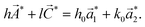
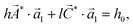
Fig. 11(a) shows a model structure of a raft-like bundle of single-walled carbon nanotubes. All nanotubes have similar diameter and are closed hexagonal packed. Fig. 11(b) is an electron micrograph of such a raft-like bundle of single-walled carbon nanotubes produced by single-beam laser evaporation.90 There are about fifty nanotubes of about the same diameter in this bundle. Fig. 11(c) is an experimental electron diffraction pattern obtained from the bundle of nanotubes.38 Letters A and Z indicate the positions of the reflection peaks from the armchair and zigzag nanotubes, respectively. The continuous distribution along the (10) and (11) reflection arcs are symmetrical about the tubule axis, indicating that the scattering tubules possess a rather uniform distribution of helicity. The electron diffraction can be calculated using a simplified model, as shown in Fig. 12(a). In this model, nine nanotubes of about the same diameter (∼1.4 nm) are arranged in hexagonal closed packing. The electron diffraction intensity distribution is displayed in Fig. 12(b). As expected, the intensities are distributed rather evenly between the positions corresponding to the zigzag and the armchair structures.
 |
| | Fig. 12 (a) A model structure composed of nine carbon nanotubes of about the same diameter. The chiral indices of each nanotube are also given in the figure. (b) Calculated electron diffraction pattern of the model structure. Continuous distribution of scattering intensities is formed due to the rather uniform distribution of helicity in the nanotubes.79 | |
Fig. 13 shows an electron diffraction pattern of a double-walled carbon nanotube.79 As can be seen from the pattern, there are now six pairs of principal layer lines across the equatorial layer line due to the two shells of the nanotube. The two sets of electron diffraction patterns are indicated by arrows in the figure. The chiral indices of the two shells are determined to be (15,11) and (30,3), respectively. Their diameter and helicity are (1.770 nm, 24.92°) and (2.475 nm, 4.72°), respectively, with an inter-layer spacing of 0.355 nm.
Fig. 14 shows an electron diffraction pattern of a triple-walled carbon nanotube, where nine pairs of principal layer lines are present.79 The chiral indices of the three shells are determined to be (35,14), (37,25), and (40,34), respectively. All three shells are metallic.
 |
| | Fig. 14 Electron diffraction pattern of a triple-walled carbon nanotube. The pattern consists of three sets of individual patterns due to the three shells of the nanotube. The chiral indices of the three shells are determined to be (35,14), (37,25), and (40,34), respectively. All shells are metallic.79 | |
Fig. 15(a) shows the TEM image of a quadruple-walled carbon nanotube and the corresponding electron diffraction pattern of the nanotube is given in Fig. 15(b).50 From the TEM image shown in Fig. 15(a), we can estimate that the nanotube has an inner diameter and outer diameter of 2.6 nm and 5.0 nm, respectively. The electron diffraction pattern of this carbon nanotube, a magnified portion of which is shown in Fig. 15(c), was used to deduce the chiral indices of each and every shell of the nanotube. It is also interesting to note that there are only three different helicities by examining the number of principal layer lines indicated by the arrows in the electron diffraction pattern due to the fact that two of the four shells have the same helicity. By measuring the principal layer line spacings in the electron diffraction pattern in Fig. 15(c), the m/n ratios were obtained as 0.031, 0.642, and 0.927, corresponding to helical angles 1.53°, 22.84°, and 28.76°, respectively. Using the principal layer line l1 and the positions of the intensity peaks on this layer line, the value of index m can be deduced: m = 25 for the helicity of 22.84° and m = 24 for the helicity of 28.76°. Combining with the m/n ratios determined above, the chiral indices for these two nanotubes are assigned to be (26,24) and (39,25), respectively, which are neighboring shells in the nanotube.
 |
| | Fig. 15 (a) TEM image of a quadruple-walled carbon nanotube. (b) Corresponding electron diffraction pattern of the carbon nanotube. (c) Magnified portion of the diffraction pattern marked in (b). Only three sets of individual electron diffraction patterns can be identified due to the overlapping of the diffraction patterns of two of them, indicating that these two shells have the same helicity. (d) Side-view of the structure of the quadruple-walled carbon nanotube. (e) Cross-sectional view of the determined structure, where the chiral indices of each shell are also indicated.50 | |
Since there are four individual shells in the nanotube, two shells must have the same helicity. These two shells are identified by the modulations in the intensity distribution on the layer line marked with red arrows (helicity = 1.53°), which indicate that two nanotubes have both contributed to these layer lines and their chiral indices were determined to be (32,1) and (64,2), respectively, by making use of the geometric constraints of the concentric shells in the multi-walled carbon nanotube. Fig. 15(d) shows the determined structure in side view of the four shells of this nanotube with chiral indices (32,1), (26,24), (39,25) and (64,2), whose cross-sectional view is given in Fig. 15(e). All these shells are semiconducting. It is worth noting that the inter-tubular distances are not of the same value. They vary from 0.423 nm to 0.492 nm and to 0.358 nm from the outermost shell to innermost shell in the nanotube.
The procedure presented here for determining the atomic structure of the quadruple-walled carbon nanotube can be extended to multi-walled carbon nanotubes with fewer or more shells. With the precision given in the present measurement, up to nine shells (outer diameter up to 10 nm) have been determined unambiguously.51 Once the atomic structure of a multi-walled carbon nanotube is determined, we can predict their physical and chemical properties, including identifying which shell is metallic or semiconducting.
Conclusions
Rich information on the atomic structure is contained in the principal layer lines formed by the graphene reflections (01), (0), and (11) (l1, l2, and l3 with respective layer line spacing D1, D2 and D3) on an electron diffraction pattern of a carbon nanotube. The chiral indices of individual carbon nanotubes (n,m) can now be determined accurately using nano-beam electron diffraction. The diffraction intensities on the principal layer lines l1, l2, and l3 are proportional to the square of the Bessel functions of orders m, n, and n + m: Il1
∝ |Jm (πdR)|2,Il2
∝ |Jn (πdR)|2, and Il3
∝ |Jn+m (πdR)|2. By identifying the corresponding order of the Bessel function on the principal layer lines l1 and l2, the chiral indices (n,m) can be obtained. On the other hand, the ratio of the chiral indices can be obtained with a high accuracy from the measurable layer line spacings n/m = (2D1
−
D2)/(2D2
−
D1) and the chiral indices (n,m) could then be deduced with the aid of a chart.
Appendix
In a polar coordinate system, the coordinates (r, ϕ, z) are related to the Cartesian coordinates (x, y, z) by the following transformation| |  | (A1) |
For the coordinates in reciprocal space, the corresponding equations are| |  | (A2) |
The structure factor in the polar coordinate system is| |  | (A3) |
and this is a general expression for any object in a polar coordinate system.
Introducing the Bessel function Jn of order n defined by
| |  | (A4) |
and the following relationships:
| |  | (A5) |
| |  | (A6) |
we can obtain
| |  | (A7) |
When the potential
V(
r,
ϕ,
z) has an
N-fold rotation axis along the
z-direction,
i.e.,
| |  | (A8) |
the Fourier expansion of
V(
r,
ϕ,
z) can be written in the following form
| |  | (A9) |
where
| |  | (A10) |
and the structure factor becomes
| |  | (A11) |
If the object is periodic along the
z-direction with periodicity
c, the Fourier expansion
(eqn (A4)) can be written as
| |  | (A12) |
and we can incorporate the
z-components into the relevant equations to obtain the following expression of the structure factor:
| |  | (A13) |
Acknowledgements
The author would like to thank his former graduate student, Dr. Zejian Liu, for his contributions, including preparation of many of the figures presented in this article, and Dr. Qi Zhang for her assistance. Financial support from the W.M. Keck Foundation, the University of North Carolina at Chapel Hill (UNC) and the UNC Research Council is also gratefully acknowledged.
References
- W. H. Bragg and W. L. Bragg, Nature, 1913, 91, 557 CrossRef.
- W. H. Bragg and W. L. Bragg, Proc. Roy. Soc. (London), 1913, 89A, 277 Search PubMed.
- J. D. Bernal, Proc. R. Soc. London, Ser. A, 1924, 106, 749 CrossRef CAS.
- H. W. Kroto, J. R. Heath, S. C. O’Brien, R. F. Curl and R. E. Smalley, Nature, 1985, 318, 162 CrossRef CAS.
- W. Krätschmer, L. D. Lamb, K. Fostiropouls and D. R. Huffman, Nature, 1990, 347, 354 CrossRef.
- S. Iijima, Nature, 1991, 354, 56 CrossRef CAS.
- Y. Ando and M. Ohkochi, J. Cryst. Growth, 1982, 60, 147 CrossRef CAS.
- S. Iijima and T. Ichihashi, Nature, 1993, 363, 603 CrossRef CAS.
- D. S. Bethune, C.-H. Kiang, M. S. de Vries, G. Gorman, R. Savoy, J. Vazquez and R. Beyers, Nature, 1993, 363, 605 CrossRef CAS.
- A. M. Rao, E. Richter, S. Bandow, B. Chase, P. C. Eklund, K. A. Willams, S. Fang, K. R. Subbaswamy, M. Menon, A. Thess, R. E. Smalley, G. Dresselhaus and M. S. Dresselhaus, Science, 1997, 275, 187 CrossRef CAS.
- A. Jorio, M. A. Pimenta, A. G. Souza, R. Saito, G. Dresselhaus and M. S. Dresselhaus, New J. Phys., 2003, 5, 139 CrossRef.
- S. M. Bachilo, M. S. Strano, C. Kittrell, R. H. Huage, R. E. Smalley and R. B. Weisman, Science, 2002, 298, 2361 CrossRef CAS.
- M. S. Strano, S. K. Doorn, E. H. Haroz, C. Kittrell, R. H. Huage and R. E. Smalley, Nano Lett., 2003, 3, 1091 CrossRef CAS.
- M. Ge and K. Sattler, Science, 1993, 260, 515 CAS.
- M. Ge and K. Sattler, Appl. Phys. Lett., 1994, 65, 2284 CrossRef CAS.
- N. Lin, J. Ding, S. Yang and N. Cue, Carbon, 1996, 34, 1295 CrossRef CAS.
- J. W. G. Wildoer, L. C. Venema, A. G. Rinzler, R. E. Smalley and C. Dekker, Nature, 1998, 391, 59 CrossRef CAS.
- T. W. Odom, J.-L. Huang, P. Kim and C. M. Lieber, Nature, 1998, 391, 62 CrossRef CAS.
- W. Cochran, F. C. H. Crick and V. Vand, Acta Crystallogr., 1952, 5, 581 CrossRef CAS.
- J. D. Watson and F. C. H. Crick, Nature, 1953, 171, 737 CAS.
- M. H. F. Wilkins, A. R. Stokes and H. R. Wilson, Nature, 1953, 171, 738 CAS.
- R. Franklin and R. Gosling, Nature, 1953, 171, 739.
- A. Klug, F. H. C. Crick and H. W. Wyckoff, Acta Crystallogr., 1958, 11, 199 CrossRef CAS.
-
B. K. Vainshtein, Diffraction of X-Rays by Chain Molecules, Elsevier Publishing, Amsterdam, 1966 Search PubMed.
-
D. Sherwood, Crystals, X-Rays and Proteins, Longman, London, 1996 Search PubMed.
- L.-C. Qin, J. Mater. Res., 1994, 9, 2450 CrossRef CAS.
- A. A. Lucas, V. Bruyninckx and P. h. Lambin, Europhys. Lett., 1996, 35, 355 CrossRef CAS.
- P. Lambin and A. A. Lucas, Phys. Rev., 1997, B56, 3571 Search PubMed.
- A. A. Lucas and P. Lambin, Rep. Prog. Phys., 2005, 68, 1181 CrossRef CAS.
- X. F. Zhang, X. B. Zhang, G. Van Tendeloo, S. Amelinckx, M. Op de Beeck and J. Van Landuyt, J. Cryst. Growth, 1993, 130, 368 CrossRef CAS.
- X. B. Zhang, X. F. Zhang, S. Amelinckx, G. Van Tendeloo and J. Van Landuyt, Ultramicroscopy, 1994, 54, 237 CrossRef CAS.
- X. B. Zhang and S. Amelinckx, Carbon, 1994, 32, 1537 CrossRef CAS.
- S. Amelinckx, B. Devouard and A. Baronnet, Acta Crystallogr., 1996, A52, 850 CrossRef CAS.
- D. Bernaerts, S. Amelinckx, P. Lambin and A. A. Lucas, Appl. Phys. A: Mater. Sci. Process., 1998, 67, 53 CrossRef CAS.
- S. Amelinckx, A. Lucas and P. Lambin, Rep. Prog. Phys., 1999, 62, 1471 CrossRef CAS.
- L.-C. Qin, T. Ichihashi and S. Iijima, Ultramicroscopy, 1997, 67, 181 CrossRef CAS.
- J. M. Cowley, P. Nikolaev, A. Thess and R. E. Samlley, Chem. Phys. Lett., 1997, 265, 379 CrossRef CAS.
- L.-C. Qin, S. Iijima, H. Kataura, Y. Maniwa, S. Suzuki and Y. Achiba, Chem. Phys. Lett., 1997, 268, 101 CrossRef CAS.
- L.-C. Qin, Chem. Phys. Lett., 1998, 297, 23 CrossRef CAS.
- L.-C. Qin, Mater. Characterization, 2000, 44, 407 Search PubMed.
- R. R. He, H. Z. Jin, J. Zhu, Y. J. Yan and X. H. Chen, Chem. Phys. Lett., 1998, 298, 170 CrossRef CAS.
- M. Kociak, K. Suenaga, K. Hirahara, Y. Saito, T. Nagahira and S. Iijima, Phys. Rev. Lett., 2002, 89, 155501 CrossRef CAS.
- J.-F. Colomer, L. Henrard, P. Lambin and G. Van Tendeloo, Phys. Rev., 2001, B64, 125425 Search PubMed.
- J.-F. Colomer, L. Henrard, P. Lambin and G. Van Tendeloo, Euro. Phys. J., 2002, B27, 111 Search PubMed.
- M. Gao, J. M. Zuo, R. D. Twesten, I. Petrov, L. A. Nagahara and R. Zhang, Appl. Phys. Lett., 2003, 82, 2703 CrossRef CAS.
- J.-F. Colomer, L. Henrard, P. Launois, G. Van Tendeloo, A. A. Lucas and P. Lambin, Phys. Rev. B, 2004, 70, 075408 CrossRef.
- J. M. Zuo, I. Vartanyants, M. Gao, R. Zhang and L. A. Nagahara, Science, 2003, 300, 1419 CrossRef CAS.
- Z. Liu and L.-C. Qin, Chem. Phys. Lett., 2005, 408, 75 CrossRef CAS.
- Z. Liu, Q. Zhang and L.-C. Qin, Phys. Rev. B, 2005, 71, 245413 CrossRef.
- Z. Liu, Q. Zhang and L.-C. Qin, Appl. Phys. Lett., 2005, 86, 191903 CrossRef.
-
Q. Zhang, J. Tang, Z. Liu, H. Zhang, X. Zhao, Y. Ando and L.-C. Qin, Proceedings of the 16th International Microscopy Congress, 2006, p. 1312 Search PubMed.
- M. Liu and J. M. Cowley, Carbon, 1994, 32, 393 CAS.
- M. Liu and J. M. Cowley, Ultramicroscopy, 1994, 53, 333 CrossRef CAS.
- X. D. Fan and L. A. Bursil, Philos. Mag., 1995, A72, 139 Search PubMed.
- L. Margulis, P. Dluzewski, Y. Feldman and R. Tenne, J. Microsc., 1996, 181, 68 CAS.
- D. Bernaerts, A. Zettl, N. G. Chopra, A. Thess and R. E. Smalley, Solid State Commun., 1998, 105, 145 CrossRef CAS.
- K. Hirahara, S. Bandow, K. Suenaga, H. Kato, T. Okazaki, H. Shinohara and S. Iijima, Phys. Rev. Lett., 2000, 85, 5384 CrossRef CAS.
- P. Lambin, V. Meunier, L. Henrard and A. A. Lucas, Carbon, 2000, 38, 1713 CrossRef CAS.
- L. Henrard, A. Loiseau, C. Journet and P. Bernier, Eur. Phys. J., 2000, B13, 661.
- A. A. Lucas, F. Moreau and P. Lambin, Rev. Mod. Phys., 2002, 74, 1 CrossRef CAS.
- R. R. Schlittler, J. W. Seo, J. K. Gimzewski, C. Durkan, M. S. M. Saifullah and M. E. Welland, Science, 2001, 292, 1136 CrossRef CAS.
- M. F. Chisholm, Y. H. Wang, A. R. Lupini, G. Eres, A. A. Puretzky, B. Brinson, A. V. Melechko, D. B. Geohegan, H. T. Cui, M. P. Johnson, S. J. Pennycook, D. H. Lowndes, S. C. Arepalli, C. Kittrell, S. Sivaram, M. Kim, G. Lavin, J. Kono, R. Hauge and R. E. Smalley, Science, 2003, 300, 1236 CAS.
- J. C. Meyer, M. Paillet, G. S. Duesberg and S. Roth, Ultramicroscopy, 2006, 106, 76.
- M. Kociak, K. Hirahara, K. Suenaga and S. Iijima, Eur. Phys. J., 2003, B32, 457 Search PubMed.
- W. Ruland, A. K. Schaper, H. Hou and A. Greiner, Carbon, 2003, 41, 423 CrossRef CAS.
- J.-F. Colomer, L. Henrard, G. Van Tendeloo, A. A. Lucas and P. Lambin, J. Mater. Chem., 2004, 14, 603 RSC.
- G. Y. Zhang, X. Jiang and E. G. Wang, Science, 2003, 300, 472 CrossRef CAS.
-
(a) J. Luo, J. Zhu and H. Q. Ye, Science, 2004, 303, 766c CrossRef;
(b) G. Y. Zhang, X. D. Bai, X. Jiang and E. G. Wang, Science, 2004, 303, 766d CrossRef.
- K. Hirahara, S. Bandow, H. Kataura, M. Kociak and S. Iijima, Phys. Rev. B, 2004, 70, 205422 CrossRef.
- J. C. Meyer, M. Paillet, G. S. Duesberg and S. Roth, Ultramicroscopy, 2005, 106, 176.
- Z. Liu and L.-C. Qin, Chem. Phys. Lett., 2004, 400, 430 CrossRef CAS.
- Z. Liu and L.-C. Qin, Chem. Phys. Lett., 2005, 402, 202 CrossRef CAS.
- Z. Liu and L.-C. Qin, Chem. Phys. Lett., 2005, 405, 265 CAS.
- Z. Liu and L.-C. Qin, Chem. Phys. Lett., 2005, 406, 106 CrossRef CAS.
- Z. Liu and L.-C. Qin, Chem. Phys. Lett., 2005, 411, 291 CrossRef CAS.
- Z. Liu and L.-C. Qin, Chem. Phys. Lett., 2005, 412, 399 CrossRef CAS.
- L.-C. Qin and S. Iijima, Mater. Res. Soc. Symp. Proc., 2000, 593, 33 CAS.
- Z. Liu and L.-C. Qin, Carbon, 2005, 43, 2146 CrossRef CAS.
-
Z. Liu, PhD thesis, University of North Carolina at Chapel Hill, 2005.
- J. C. Meyer, M. Paillet and S. Roth, Science, 2005, 309, 1539 CrossRef CAS.
- J. Zhang and J. Zhu, Chem. Phys. Lett., 2006, 420, 171 CrossRef CAS.
- M. Y. Sfeir, T. Beetz, F. Wang, L. M. Huang, X. M. H. Huang, M. Y. Huang, J. Hone, S. O’Brien, J. A. Misewich, T. F. Heinz, L. J. Wu, Y. M. Zhu and L. E. Brus, Science, 2006, 312, 554 CrossRef CAS.
- Z. Xu, X. D. Bai, Z. L. Wang and E. G. Wang, J. Am. Chem. Soc., 2006, 128, 1052 CrossRef CAS.
- H. Jiang, D. P. Brown, A. G. Nasibulin and E. I. Kauppinen, Phys. Rev. B, 2006, 74, 035427 CrossRef.
- H. Jiang, D. P. Brown, A. G. Nasibulin and E. I. Kauppinen, Carbon, 2006 DOI:10.1016/j.carbon.2006.07.025.
-
R. Saito, G. Dresselhaus and M. S. Dresselhaus, Physical Properties of Carbon Nanotubes, Imperial College Press, London, 1998 Search PubMed.
-
M. Abramovitz and I. A. Stegun, Handbook of Mathematical Functions, National Bureau of Standards, Washinton, DC, 1972 Search PubMed.
- L.-C. Qin, Rep. Prog. Phys., 2006, 69, 2761 CrossRef.
- A. Thess, R. Lee, P. Nikolaev, H. J. Dai, P. Petit, J. Robert, C. H. Xu, Y. H. Lee, S. G. Kim, A. G. Rinzler, D. T. Colbert, G. E. Scuseria, D. Tomanek, J. E. Fischer and R. E. Smalley, Science, 1996, 273, 483 CrossRef CAS.
- L.-C. Qin and S. Iijima, Chem. Phys. Lett., 1997, 269, 65 CrossRef CAS.
- C. Journet, W. K. Maser, P. Bernier, A. Loiseau, M. Lamy de la Chapelle, S. Lefrant, P. Deniards, R. Lee and J. E. Fischer, Nature, 1997, 388, 756 CrossRef CAS.
|
| This journal is © the Owner Societies 2007 |
Click here to see how this site uses Cookies. View our privacy policy here. 

