Tuning plasmons on nano-structured substrates for NIR-SERS
Sumeet
Mahajan
a,
Mamdouh
Abdelsalam
a,
Yoshiro
Suguwara
b,
Suzanne
Cintra
a,
Andrea
Russell
a,
Jeremy
Baumberg
b and
Philip
Bartlett
*a
aSchool of Chemistry, University of Southampton, Southampton, UK SO17 1BJ. E-mail: pnb@soton.ac.uk; Fax: +44-23-8059-3781; Tel: +44-23-8059-3333
bSchool of Physics and Astronomy, University of Southampton, Southampton, UK SO17 1BJ. Fax: +44-23-8059-2093; Tel: +44-23-8059-2094
First published on 23rd November 2006
Abstract
Surface-Enhanced Raman Spectroscopy (SERS) is a very sensitive and selective technique for detecting surface species. Colloidal crystal-templated ‘inverse opal’ nanostructured gold films have been demonstrated to be excellent SERS substrates by various researchers around the globe. However, visible excitation laser sources commonly used in SERS experiments can cause photochemical reactions on the surface as well as fluorescence from the adsorbed molecules. A way to circumvent this possibility is the use of Near Infra-Red (NIR) laser sources. This demands appropriate design of substrates for NIR-SERS in order to obtain maximum enhancement of signals from analytes. In the current paper, we use systematic variation of sphere size and electrochemical control over film height to tune plasmons on such nanovoid substrates. We use plasmon maps as a tool for predicting NIR-SERS enhancements recorded with a 1064 nm laser source for benzenethiol as the probe molecule. Direct correlation is observed between Raman enhancements and plasmonic resonances with ingoing and outcoming radiation. Our study demonstrates the feasibility of plasmon engineering and the predictive power of their mapping on our substrates. It also demonstrates the ability to design reproducible NIR-SERS substrates and its empirical fruition.
Introduction
Plasmon-active materials are being intensely investigated owing to their wide ranging applications.1 One of the most promising is their application in Surface-Enhanced Raman Scattering (SERS).2 SERS is an extremely sensitive and selective technique for detecting surface species. Most of the signal enhancement in SERS compared to conventional Raman is attributed to the large increase in the local electric field generated.3 Since plasmons lead to such field enhancements, surfaces that support various plasmon modes could serve as SERS active substrates. However, the ability to produce such structures reproducibly is critical to their exploitation.In recent years, we have demonstrated the ability to make reproducible nanostructured substrates using colloidal crystal-templated electrodeposition .4,5 Colloidal crystal-templated ‘inverse opal’ nanostructured gold films have been demonstrated to be excellent SERS substrates.6–8 Further, though the optical and enhancement properties of SERS substrates have been found to be structure dependent,9,10 no reports exist wherein such nanovoid substrates are targeted and tailored for use with a particular excitation wavelength, especially in the NIR region.
We have shown recently that plasmon modes on such nanovoid substrates can be tuned as a function of sphere size and film height.11,12 Further, the relationship between SERS and resonance of ingoing laser excitation and outcoming scattered radiation bearing the signature of the molecule with plasmons on these nanovoid substrates has been probed.8,13 The inter-dependence of optical properties, plasmon modes and SERS implies that it would be imperative to design substrates for use with a particular excitation laser and target molecule for optimum SERS.
A typical SERS experiment is carried out using a visible laser. This can cause photochemical reactions, interference due to fluorescence, and degeneration, especially of large biological molecules.14 Hence, the need for benign sources of excitation for SERS of biological molecules necessitates tailored substrates for Near Infra-Red (NIR) wavelengths and the particular analyte under investigation. In this report, we demonstrate the predictive power of plasmon mapping and its use as a design tool for engineering substrates for NIR-SERS. This represents the first report demonstrating the tunability and experimental realization of colloidal-templated gold ‘inverse opals’ for NIR-SERS using a 1064 nm laser source.
Experimental details
Preparation of nanostructured substrates
Substrates were prepared following the previously published method by Bartlett et al.4,10 A typical synthesis of a substrate involves preparation of conductive surfaces by thermal vapour deposition of a 10 nm layer of chromium, followed by 200 nm of gold on to glass slides. These gold surfaces were used, after treatment with 10 mM cysteamine solution in ethanol for 48 h, for electrodeposition of gold through a template of polystyrene latex spheres assembled on the surface. The spheres were obtained as 1 wt % aqueous solutions from Duke Scientific Corp. The assembly was carried out in a manner such that a monolayer template of hexagonally packed, well-ordered spheres was obtained. Gold was electrochemically grown from a commercial cyanide-free gold plating solution (Tech. Gold 25, Technic Inc.). After the electrodeposition , the polymer spheres were removed by dissolving in DMF. This resulted in substrates with an array of interconnected voids of varying depth depending on the charge passed during the electrodeposition .In the current study, substrates were prepared with a range of sphere diameters from 700 nm to 1100 nm. Substrates were prepared in which the film height was graded by retracting the template from the plating solution in incremental steps using a micrometer stage. In the current report the film heights quoted are as estimated from their pore-mouth diameters, as described by Bartlett et al.10
Structure determination
The structure and morphology of the templated films were investigated using Philips XL30 Environmental Scanning Electron Microscope (ESEM). Representative SEM images presented in Fig. 1 for substrates prepared with 900 nm Diameter (D) sphere templates show that uniform gold films were obtained with almost negligible defects. | ||
Fig. 1
SEM images of a graded gold film fabricated using 900 nm D sphere template recorded at various film heights. Images corresponding to film thicknesses of: (a) 0.25 D; (b) 0.45 D; (c) 0.7 D; and (d) 0.9 D are shown. All images were obtained under 10![[thin space (1/6-em)]](https://www.rsc.org/images/entities/char_2009.gif) 000 magnification. The scale bar for the images is 2 µm. 000 magnification. The scale bar for the images is 2 µm. | ||
High resolution images were obtained with a Jeol JSM 6500 F thermal Field Emission Scanning Electron Microscope (FESEM). FESEM images obtained of both the evaporated gold, upon which the substrates are grown, and an electrochemically deposited substrate are presented in Fig. 2. The images were obtained using the same magnification and it can be clearly seen that the electrodeposited substrate is much smoother in comparison to the evaporated film. Samples prepared in this way were subjected to reflectance measurements and spectra were obtained. Thereafter, FT-Raman spectra were recorded on the sample from approximately the same positions as the reflectance spectra.
 | ||
| Fig. 2 FESEM images showing the smoothness of (b) electrodeposited structured film compared to (a) flat evaporated gold used as substrate. Evaporated gold also visible in the middle at the bottom of the voids is clearly rougher than electrodeposited structured gold film. The voids shown in (b) correspond to a film height of 0.9 D templated with 900 nm spheres. The scale bar for both images is 200 nm. | ||
Reflectance and SERS measurements
The reflectivity of samples prepared as described above was studied using a BX51TRF Olympus microscope illuminated with an incoherent white light source coupled to an Ocean Optics NIR 512 (850–1800 nm) spectrometer. The spectra were recorded in the normal incidence mode. A 20X IR objective with a numerical aperture of 0.40 was used to record the spectra. All spectra were normalized with respect to that recorded on flat gold deposited on glass slides by vapour deposition. Gold was chosen for normalization as its absorbance is fairly constant over the wavelength range studied and it is chemically stable. A CCD camera (Olympus DP2) mounted on the microscope enabled the simultaneous recording of optical images of the area whose spectrum was being monitored. NIR-SERS measurements were made using a Perkin Elmer System 2000 FTIR spectrometer with an FT-Raman attachment equipped with a 1064 nm Nd:YAG laser. Raman spectra were recorded in the back-scattered geometry between 200 cm–1 to 3500 cm–1 wavenumber shift using an indium–gallium–arsenide (InGaAs) detector. A spectral resolution of 4 cm–1 was used with the incident laser power at the sample measured to be 250 mW. For all spectra, 50 scans were averaged.Results and discussion
Reflectance spectra were recorded, in the normal incidence and back reflection geometry with the apparatus described above, on gold films templated with different sphere sizes. Cintra et al. have shown that the various plasmon modes generated on nanostructured gold substrates gradually red shift as the sphere diameters are increased from 350 nm to 800 nm.8 Therefore, by increasing the sphere sizes further we expected to generate plasmons at NIR wavelengths. Hence, in the present study, sphere diameters of 700, 800, 900, 1000 and 1100 nm were used. The reflectance recorded from graded gold films was normalized with respect to evaporated flat gold, as in the NIR region gold has an almost negligible and wavelength-independent absorbance. The spectra for the graded 800 nm sphere-templated substrate are presented on a logarithmic scale (analogous to absorbance) with the normalized reflectance being plotted against wavelength in Fig. 3a. For visualizing the plasmon resonances that occur on the substrates, the same data is presented as an extinction map in Fig. 3b. Extinction, being the sum of absorbance and scattering, gives an upper bound on the extent of plasmonic interactions on the substrate. However, we have previously shown that absorption dominates on these substrates.11 Thus, Fig. 3 gives the relationship between reflectance spectra obtained at different thicknesses and the corresponding wavelength–position map showing the extent of extinction for an 800 nm sphere-templated graded gold film. | ||
| Fig. 3 Data obtained from reflectance measurements at different film thicknesses on a graded gold film is converted to an extinction intensity map. In (a), reflectance spectra recorded at different film thicknesses on a graded gold film templated with 800 nm spheres are offset for clarity. The film heights in the figure, shown under each spectrum, increase from top to bottom. R and R0 are reflection intensities obtained from the nanostructured film and flat gold, respectively. The corresponding extinction intensity contour map is shown in (b). The dips correspond to the bright areas. The extinction intensity is normalized with respect to flat gold. Red indicates a maximum of 1 and violet stands for the least (complete reflection) extinction of 0 with respect to flat gold. The extinction intensity maps relate directly (with an element of over-estimation, as extinction could occur due to scattering as well) to possible plasmonic resonances on the substrate as a function of film height. The film thickness is normalized with respect to sphere diameter. | ||
Extinction maps in the NIR range of 850 to 1800 nm were obtained for graded gold nanovoid films templated with 700 nm, 800 nm, 900 nm, 1000 nm and 1100 nm diameter spheres. The maps for 700, 900 and 1100 nm sphere-templated gold films are shown in Fig. 4. Localized plasmons have been shown to exist at ∼0.6 D for our nanostructured substrates.15 This appears as a weak band for the 700 nm nanovoid film, as evident in Fig. 4a. This band undergoes a red shift on increasing the sphere size to 900 and 1100 nm (Fig. 4b and c). The extent of absorption is largest for 900 nm sphere-templated films compared to the 700 nm and 1100 nm substrates. Extinction maps with 800 and 1000 nm sphere-templated films display the same trend and, hence, have not been included in this figure. One can also see Bragg plasmons11,13 emerging in the NIR region, centered around 900 nm and 1100 nm in Fig. 4b and c, respectively, corresponding to the grating-like behaviour of shallow dishes.
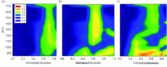 | ||
| Fig. 4 Extinction contour maps for (a) 700 nm, (b) 900 nm and (c) 1100 nm sphere-templated gold nanostructured films. All maps are colour-coded using the same spectrum scale of 0 (violet) to 1 (red), as in Fig. 3. The film heights are normalized with respect to sphere diameter. | ||
Raman spectra of adsorbed benzenethiol were obtained as a function of position (film height) using the same substrates that were studied by reflectance . The spectrum for benzenethiol obtained at ∼0.75 D using the 800 nm sphere-templated sample is shown in Fig. 5a. The peak assignments indicated in the figure are based on those reported by Han et al.16 The absence of a peak associated with the ν(S–H) stretching vibration confirms the formation of no more than a monolayer of adsorbed benzenethiol and its linkage with gold; the S–H bond is cleaved when the Au–S bond forms. All samples were treated with benzenethiol solutions for 24 h and dried under argon before recording the SERS spectra. No significant increase in SERS intensities were observed on increasing the exposure time to 48 h. The SERS enhancement factors were determined by comparison to the spectrum of neat benzenethiol and assuming the formation of a compact monolayer, as described previously.8,17 The enhancement factor of the ∼0.75 D 800 nm substrate corresponding to the spectrum shown in Fig. 5a was calculated to be 2.6 × 10⁶. The SERS from the substrates were stable and repeatable: thus, the standard deviation was found to be less than 6.3 % for spectra (n = 14) recorded from approximately the same position (within 0.5 mm) on different occasions over several days.
 | ||
| Fig. 5 Spectrum of benzenethiol adsorbed on (a) 800 nm sphere-templated gold film at 0.75 D film height, showing the absence of an –SH peak. The SERS spectra recorded at different film heights for: (b) 700 nm; (c) 900 nm; and (d) 1100 nm sphere-templated gold films. The peak intensities pass through a maximum with respect to film height. The enhancements are most pronounced in (c), in which the intensity scale is 0–15, while in (a) and (d) it is 0–4 AU. The spectra were recorded with an FT-Raman spectrometer equipped with a 1064 nm Nd:YAG laser. 50 scans were averaged under a laser incident power of 250 mW at the sample. Spectral resolution was 4 cm–1. | ||
The SERS spectral profiles with respect to film height for 700, 900 and 1100 nm sphere-templated substrates are shown in Fig. 5b–d. The variation of SERS signals with sphere diameter of the template and film height is clearly evident. The intensity of peaks in the SERS spectra exhibit a strong dependence on the thickness of the film as well as the sphere diameter used for templating the structure. The maximum enhancements occur between 0.4 and 0.8 D depending on the templating sphere diameter. Among all the samples, the greatest SERS enhancements were obtained with the 900 nm sphere-templated nanovoid film at around ∼0.6 D. The enhancement factor18 was calculated to be 3 × 10⁶, which was the highest among the substrates in this study. The 800 nm sphere-templated film showed a SERS enhancement profile similar to that of the 700 nm sphere-templated film, with the maximum signal being obtained at ∼0.75 D, albeit with much higher intensities. The enhancement factor for the 800 nm nanovoid film at ∼0.75 D thickness was only slightly lower than that obtained for the 900 nm film at ∼0.6 D. The 1000 nm nanovoid film behaved very similarly to the 1100 nm sphere-templated film and showed very little SERS enhancement.
To understand the origin of such structural dependence of Raman enhancements, we carried out plasmon mapping and SERS spectral profiling on all substrates from 700 to 1100 nm sphere-templated structured films and studied them in tandem. As expected, the SERS enhancement was higher at those film thicknesses where existence of a plasmon mode was indicated on the extinction map compared to those where a weak or no plasmonic interaction was observed. However, the effect is more subtle than this. On overlaying the SERS intensities corresponding to 420 cm–1, 997 cm–1 and 1570 cm–1 Raman bands of benzenethiol at the appropriate outcoming wavelengths on the extinction maps along with the ingoing excitation laser, we can see an obvious correlation (Fig. 6). Wherever both the ingoing and outcoming wavelengths matched with strong extinction on the substrate, we can see a large enhancement in SERS.
 | ||
Fig. 6 Extinction intensity contour maps superimposed with Raman scattering peak intensities for gold substrates templated with: (a) 700 nm; (b) 800 nm; (c) 900 nm; (d) 1000 nm; and (e) 1100 nm spheres. ( ) denotes the ingoing laser excitation at 1064 nm in the NIR-SERS experiment. ( ) denotes the ingoing laser excitation at 1064 nm in the NIR-SERS experiment. ( ), ( ), ( ) and ( ) and ( ) represent the outcoming radiation at 1114 nm, 1191 nm and 1277 nm corresponding to 420 cm–1, 1000 cm–1 and 1570 cm–1 Raman bands of benzenethiol, respectively. The lengths of the arrows indicate the intensity of the scattered radiation (on a scale of 0 to 8.5 AU). ) represent the outcoming radiation at 1114 nm, 1191 nm and 1277 nm corresponding to 420 cm–1, 1000 cm–1 and 1570 cm–1 Raman bands of benzenethiol, respectively. The lengths of the arrows indicate the intensity of the scattered radiation (on a scale of 0 to 8.5 AU). | ||
The matching of wavelengths correspond to the desired resonance coupling between the laser excitation as well as scattered radiation with the plasmons generated on the structured nanovoid surface and, hence, a large increase in SERS. Existence of plasmon modes on the structured substrates not only helps in the coupling of energy between ingoing radiation with the molecule adsorbed on the surface, but also assists in the coupling of scattered radiation back from the surface. Hence, resonance between ingoing excitation and outcoming scattered radiation with plasmon modes on the surface is critical for optimization of SERS. For the 700 nm sphere-templated film, Fig. 6a, the plasmon resonances are not strong enough in the NIR; consequently, they do not contribute to large NIR-SERS enhancement. Nevertheless, the maximum enhancements do occur when the ingoing and outcoming radiation resonates with the plasmons on the substrate. The effect of matching the incident and exiting radiation with plasmon modes is most pronounced in Fig. 6b and c for 800 and 900 nm sphere-templated structured films. Large signal enhancement occurs on resonance between strong plasmonic absorption on the surface with the ingoing and outcoming radiation. The importance of plasmon resonances with both incoming and outgoing radiation can be gauged from Fig. 6d and e, where either the ingoing or outcoming radiation, or both, are not able to couple with plasmonic resonances on the surface and therefore there is reduced SERS enhancement.
In this study we have shown the scalability of the plasmon engineering approach into the NIR region. Although it is a matter of further study on our part as to what part of our nano-structured film contributes to the plasmon modes in the NIR energy range, it is clear that we can control the generation of suitable plasmon modes by varying parameters like the sphere size and film height. With respect to the latter control, electrodeposition appears much more powerful than other techniques of metal deposition such as nanoparticle-assisted6,7 or vapour deposition.19,20 In addition, our high resolution FESEM images show that electrodeposited films are much smoother than the vapour deposited gold. The flat evaporated gold films yield no SERS, hence, we conclude that it is the macro-structure of the templated films that is responsible for SERS rather than generation of nanometer scale surface roughness or ‘hot spots’. This option of tuning plasmons on colloidal-templated nanostructured films offers an unprecedented tool for designing and tailoring substrates for obtaining SERS with a particular excitation source and a target analyte molecule.
Conclusions
In the present study, we have used variation in sphere size of colloidal templates and electrochemical control over film height to tune substrates for NIR-SERS in conjunction with a 1064 nm laser source for a particular probe molecule, in this case benzenethiol. Proper combination of the two parameters of sphere size and film height resulted in significant enhancement of signals from the adsorbed analyte. We have demonstrated the effect of matching incident and scattered radiation with plasmonic resonances on the enhancement of Raman bands of benzenethiol adsorbed on our nanostructured gold substrates. SERS intensities could be significantly improved by designing substrates that can sustain plasmonic resonances to couple with the ingoing and outcoming radiation. Our study proves the feasibility of the design, and the experimental realization, of reproducible NIR-SERS substrates.References
- W. I. Barnes, A. Dereux and T. W. Ebbesen, Nature, 2003, 424, 824–830 CrossRef CAS.
- Z. Q. Tian, J. Raman Spectrosc., 2005, 36, 466–470 CrossRef CAS.
- K. Kneipp, H. Kneipp, I. Itzkan, R. R. Dasari and M. S. Feld, J. Phys.: Condens. Matter, 2002, 14, R597–R624 CrossRef CAS.
- P. N. Bartlett, P. R. Birkin and M. A. Ghanem, Chem. Commun., 2000, 1671–1672 RSC.
- M. E. Abdelsalam, P. N. Bartlett, J. J. Baumberg, S. Cintra, T. A. Kelf and A. E. Russell, Electrochem. Commun., 2005, 7, 740–744 CrossRef CAS.
- P. M. Tessier, O. D. Velev, A. T. Kalambur, J. F. Rabolt, A. M. Lenhoff and E. W. Kaler, J. Am. Chem. Soc., 2000, 122, 9554–9555 CrossRef CAS.
- P. M. Tessier, O. D. Velev, A. T. Kalambur, A. M. Lenhoff, J. F. Rabolt and E. W. Kaler, Adv. Mater., 2001, 13, 396–400 CrossRef CAS.
- S. Cintra, M. Abdelsalem, P. N. Bartlett, J. J. Baumberg, T. Kelf, Y. Sugawara and A. E. Russell, Faraday Discuss., 2005, 132, 1–9 Search PubMed.
- R. C. Schroden, M. Al-Daous, C. F. Blanford and A. Stein, Chem. Mater., 2002, 14, 3305–3315 CrossRef CAS.
- P. N. Bartlett, J. J. Baumberg, S. Coyle and M. E. Abdelsalam, Faraday Discuss., 2004, 125, 117–132 RSC.
- T. A. Kelf, Y. Sugawara, J. J. Baumberg, M. Abdelsalam and P. N. Bartlett, Phys. Rev. Lett., 2005, 95, 116802 CrossRef CAS.
- S. Coyle, M. C. Netti, J. J. Baumberg, M. A. Ghanem, P. R. Birkin, P. N. Bartlett and D. M. Whittaker, Phys. Rev. Lett., 2001, 8717.
- J. J. Baumberg, T. Kelf, Y. Sugawara, S. Cintra, M. Abdelsalam, P. N. Bartlett and A. E. Russell, Nano Lett., 2005, 5, 2262–2267 CrossRef CAS.
- P. Hendra, C. H. Jones and G. M. Warnes, Fourier Transform Raman Spectroscopy—Instrumentation and Chemical Applications, Ellis Horwood Limited, Chichester, 1991 Search PubMed.
- T. A. Kelf, Y. Sugawara, R. M. Cole, J. J. Baumberg, M. E. Abdelsalam, S. Cintra, S. Mahajan, A. E. Russell and P. N. Bartlett, Phys. Rev. B, 2006 Search PubMed , accepted.
- S. W. Han, H. J. Lee and K. Kim, Langmuir, 2001, 17, 6981–6987 CrossRef CAS.
- J. C. Love, L. A. Estroff, K. J. K. R. G. Nuzzo and G. M. Whitesides, Chem. Rev., 2005, 105, 1103–1169 CrossRef CAS.
- Enhancement Factors (EF) were calculated by comparing the intensity of the SERS spectra to those for neat benzene thiol. The expression for the enhancement factor is EF = IsurfAmVlρNA/IbulkAlRMbt, where Isurf is the intensity of the benzenethiol peak for the substrate, Am is the area occupied by an adsorbed thiol molecule (from ref. 17), Vl is the laser volume for the bulk experiment, NA is Avogadro’s number, ρ is the density of neat benzenethiol, Ibulk is the intensity of neat benzenethiol peak, Al is laser spot area, R is the geometrical roughness factor for the surface due to the templated structure (1 ≤ R ≤ 4.63) and Mbt is the molecular weight of benzenethiol.
- J. C. Hulteen, D. A. Treichel, M. T. Smith, M. L. Duval, T. R. Jensen and R. P. Van Duyne, J. Phys. Chem. B, 1999, 103, 3854–3863 CrossRef CAS.
- T. R. Jensen, G. C. Schatz and R. P. Van Duyne, J. Phys. Chem. B, 1999, 103, 2394–2401 CrossRef CAS.
| This journal is © the Owner Societies 2007 |