Reflective thermal lens detection device
Kazuma
Mawatari†
and
Koji
Shimoide
*
Central Research Laboratory, Asahi Kasei Corporation, 2-1 Samejima, Fuji, Shizuoka 416-8501, Japan. E-mail: shimoide.kb@om.asahi-kasei.co.jp; Fax: +81-545-62-2149; Tel: +81-545-62-3104
First published on 5th December 2005
Abstract
A reflective thermal lens detection device was developed for realizing a portable and sensitive detector for a microsystem. An aluminum mirror was formed on the main plate of a microchip, and a reflected probe beam was detected with a single pick-up unit. The background signal due to light absorption of the aluminum mirror was 60 times reduced when the microchannel and the mirror were separated with an interval of 600 µm. The tilt angle of the microchip significantly affected the precision of the measurement. Then a quadrant photodiode was used to detect the center of gravity of the reflected probe beam to regulate the tilt angle within ±0.05°, and this value was enough to achieve 1% CV (coefficient of variance) precision in the measurements. The limit of detection (LOD) was 60 nM for xylene cyanol solution, and the absorbance was 9.4 × 10⁻⁶ AU. About 40 times higher sensitivity was obtained in comparison with a spectrophotometer.
Introduction
Microsystems are recognized as one of the key technologies for future progress in chemical and biochemical analytical systems such as point of care (POC) clinical diagnosis. The advantages of miniaturization include less sample and reagent volume, effective reaction due to large surface-to-volume ratio, less space requirement and low cost. These miniaturized systems require sophisticated microfabrication, microfluidics and detection technologies; especially, they put higher demands on the detection technology due to the small volume and short optical path length of the microchannels as a consequence. Therefore, a sensitive detection method is desirable in combination with wide applicability. The most sensitive method is laser-induced fluorescence (LIF), where a single molecule in a microchannel can be detected in optimum conditions.1 However, most molecules exhibit low fluorescence yield and cannot be detected by the LIF method. Derivatization reactions are not always available for the analytes of interest and result in less precise quantification due to the matrix effect. Absorption spectrometry is promising for wide applicability because various assays for colorimetric detection have already been established in environmental analysis, clinical diagnosis, and so on. However, the sensitivity is quite low for measurements in a microchannel due to a shorter optical path length of one or two orders than that of conventional cuvettes.Thermal lens spectrometry (TLS) is one of the candidates for improving the low sensitivity of absorption spectrometry.2 TLS has been developed for trace analysis in liquids on a macroscopic scale since the end of the 1970's.3–8 Kitamori's group realized a first coaxial dual-beam thermal lens microscope (TLM) that utilized an objective lens with chromatic aberration,9,10 and sensitive thermal lens detections on microchips were achieved.11,12 Then, TLM has been successfully applied to various integrated analytical systems on microchips such as environmental analysis, medical diagnosis and single cell analysis.13–17
Original TLM was a microscope-based system, and the resulting system size was large compared with the small microchip. Recently, miniaturization of the TLM system is under progress to realize practical TLM systems for microsystems. For example, Kitamori's group reported a palm-top sized thermal lens optical system utilizing a rod lens and related optical fiber technologies.18,19 In a previous paper, our group also reported a portable TLM.20 The feature of our system was a high precision focusing system because the TLM system needed accurate positioning of the excitation or probe beams for precise measurements.
Those previously reported systems were realized in a transmissive optical geometry; the change of an optical path in the transmitted probe beam was detected as thermal lens signals. However, the optical geometry requires precise and laborious alignment of the probe beam, pin-hole and a photodiode. In addition, the transmissive optical geometry occupies both of the upper and lower spaces of the small microchip. Microsystems need various and external microfluidic components like pumps, valves, temperature controllers, filters, connecters, tubes and so on. Therefore, further miniaturization of the detection device is extremely desirable for realizing a totally miniaturized system.
In this paper, we developed a reflective and portable thermal lens detection device in which laser beams were focused and detected by a single pick-up unit for the first time. We formed a thin film mirror made of aluminum on a microchip to reflect the probe beam. Firstly, large background signal due to strong light absorption by the mirror was a problem for sensitive detection. We resolved the problem by an arrangement of the mirror position. Secondly, a tilt of the microchip was found to be crucial to the measuring sensitivity. We detected the tilt angles with a quadrant photodiode and regulated the angle. The quadrant photodiode provided three functions: tilt angle detection, quantitative focusing of the laser beams and detection of the thermal lens effect. By integrating these functions on one photodiode, a precise reflective thermal lens measurement was achieved. Finally, we evaluated the sensitivity of our device from a calibration curve.
Experimental section
Optics
An optical diagram of the reflective thermal lens detection device is given in Fig. 1. (Numbers used in the component descriptions are as given in the figure.) The basic design of the pick-up unit was based on a focusing pick-up reported in our previous paper.20 A laser-diode with wavelength 635 nm (Sharp Corporation, LT051PS, output 30 mW) was used as an excitation beam, and the beam was collimated by a collimator lens. The cross section shape was made round with a prism pair (3 times magnification for the short axis of the ellipse). A laser-diode with wavelength 780 nm (Mitsubishi Electric Corporation, ML60114, output 50 mW) was used as a probe beam, and the beam was collimated by another collimator lens. The cross section shape was made round with another prism pair (2.6 times magnification for the short axis of the ellipse). A beam expander was used to adjust the focus position to enhance the sensitivity of the thermal lens signal.2 Filter 1 (Melles Griot KK, 03FCG111) was used to remove the returned excitation beam from optical components which generated a strong background signal.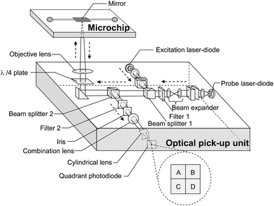 | ||
| Fig. 1 Illustration of optical arrangement of a reflective thermal lens detection device. The letters A, B, C and D denote output signals from each element of the quadrant photodiode. | ||
The excitation and probe beams were made coaxial with a beam splitter 1 (100% reflectance for the s-polarized excitation beam, 100% transmittance for the p-polarized probe beam). Then, both beams were introduced into an objective lens (numerical aperture 0.1) through a beam splitter 2 (80% transmittance and 20% reflectance for both the excitation and probe beams), prism and λ/4 plate. The λ/4 plate changed the polarization direction of the reflected laser beams by 90°, and formed part of the optical isolator.20 The excitation beam was focused into a microchannel resulting in the formation of the thermal lens effect, and the optical path of the probe beam was changed by the effect. More than 85% of the excitation and probe beams power was reflected with an aluminum mirror on the microchip and was returned to the optical pick-up unit through the objective lens.
The returned excitation and probe beams were again introduced into the beam splitter 2, and 20% of the power was reflected. The excitation beam was removed by a filter 2 (Melles Griot KK, 03FCG111), and only the probe beam was focused on a quadrant photodiode (Hamamatsu Photonics KK, S6344) after passing through an iris, combination lens (focal length 20 mm and −12 mm) and a cylindrical lens (focal length 286 mm). The output signal from the quadrant photodiode was used for focusing the laser beams,20 microchip tilt adjustment and thermal lens detection by a lock-in amplifier. In this way, the quadrant photodiode provided three important functions to realize the reflective detection as described in the previous section. The size of the pick-up unit was 15 cm × 10 cm × 3 cm.
Microchip and optical arrangement
In Fig. 2, an optical arrangement is illustrated for the excitation beam, the probe beam and the microchip. The microchip (50 mm long × 13 mm wide) was made by fused silica and consists of a cover plate (600 µm thick) and a main plate (650 µm thick). The straight and rectangular sectioned microchannel (1 mm wide × 50 µm deep × 10 mm long) was formed on the center of the main plate by sand blast etching and subsequent polishing. An aluminum mirror (1 mm wide × 10 mm long) was formed on the surface of the main plate by vacuum evaporation as shown in Fig. 2. The excitation beam was focused in the center of the microchannel. The focus of the probe beam was set at 250 µm (value in air) far from the focus of the excitation beam, and the value must be corrected as ∼356 µm in the microchip by considering the change of focusing angles due to differences of refractive indexes from that of air (1.33 for water, 1.46 for fused silica, 1.00 for air).20 The microchip was mounted on a precisely adjustable rotary and gonio stage. For focusing in the center of the microchannel, astigmatism and reflectance of the probe beam were applied for width and depth direction, respectively.20 Xylene cyanol solutions (ε = 3.0 × 10⁴ M−1 cm−1) were used as samples for all experiments.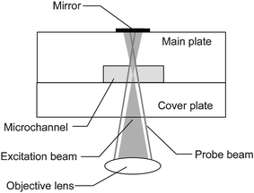 | ||
| Fig. 2 Optical configuration of an excitation beam, a probe beam and a microchip. The focal length of the probe beam was set 250 µm (a value in air) longer than that of the excitation beam. | ||
Results and discussion
Improvement of signal-to-background ratio
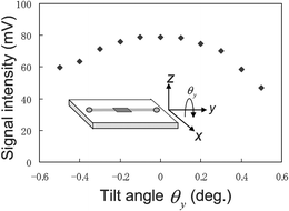
Aluminum is a cost effective material and has high reflectance (>85%) for visible wavelength light as is used in a compact disk. The loss of the optical energy is caused by absorption of light, and the absorption generates a large thermal lens signal (background signal) following photothermal conversion. In contrast to a spectrophotometer, however, TLM has spatial resolution in the depth direction of the microchannel depending on the numerical aperture of an objective lens (0.1 in this experiment). If the mirror is set a certain distance (600 µm in this experiment) from the microchannel, the background signal is expected to be ignored. Then, we investigated signal intensity dependence on the focusing positions of the excitation beam with scanning the microchip in depth directions. The sample was a 40 µM xylene cyanol solution. The result is shown in Fig. 3. The beam sizes of the excitation beam are calculated by Gaussian propagation theory2 as 7.6 µm for the beam waist and ∼130 µm for the position of 1250 µm apart from the beam waist, and the beam waist size mainly determines the strength of thermal lens effect. Three peaks were clearly observed at focusing positions of −430 µm, 0 µm and 430 µm. When the excitation beam was focused just on the aluminum mirror (0 µm position), a large background signal of 18 mV intensity was observed. The peak can be attributed to a thermal lens signal of the aluminum mirror due to strong absorption of the excitation beam. The other two peaks are derived from the absorption of light by the xylene cyanol solution in the microchannel because the two peak positions correspond to the focusing positions where the excitation beam is focused in the center of the microchannel. The mismatch of values (±625 µm calculated by main plate thickness minus half of the microchannel depth, and ±430 µm from experimental values) can be explained by the refractive index differences of water, fused silica and air, and the values of ±430 µm are reasonable by calculation with simple ray optics theory.20 The difference of the peak heights was caused by the change of probe beam power at the quadrant photodiode (0.7 V for 430 µm position and 0.6 V for −430 µm position). The phases of the three peaks from the lock-in amplifier showed approximately the same value (about −40°). For pure water (blank sample), the peak intensity at the 430 µm position was 0.3 mV, and the value was 60 times lower than the background signal at 0 µm position. Therefore, we could accomplish the high signal-to-background ratio by utilizing the spatial resolution of TLM. The optimum focusing position was 430 µm, and the position was selected for the later experiments.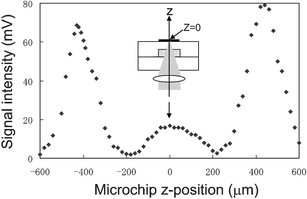 | ||
| Fig. 3 Dependence of the thermal lens signal on the z-position of the microchip. The position of z = 0 means that the excitation beam is focused just on the mirror. The sample was 40 µM xylene cyanol solution. | ||
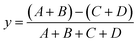
Correction of microchip tilt angle
In the development of the reflective thermal lens detection device, we found the signal intensity was very sensitive to the tilt of the microchip to a beam path. Then we investigated the signal intensity dependence on the tilt of the microchip as is shown in Fig. 4. The signal intensity decreased to ∼60% of the peak at maximum in spite of just 5% decrease of the probe beam power at the quadrant photodiode. The relative position of the iris and probe beam could be sensitive to the signal intensity. For precise measurement of 1% in coefficient of variance, the tilt angle should be within ±0.1°. For this purpose, we detected the center (X,Y) of gravity of the probe beam at the quadrant photodiode by calculating the output voltages of each quadrant photodiodes (A, B, C and D in Fig. 1). | (1) |
 | (2) |
 | ||
| Fig. 4 Dependence of the thermal lens signal on the tilt angle of the microchip. The sample was 40 µM xylene cyanol solution. | ||
The calibration curve of (X,Y) was made for θx and θy from 0 to ±0.5°. At minimum, ±0.05° could be detected, and the sensitivity was enough for ±0.1° regulations.
Limit of detection
Finally, the limit of detection (LOD) was determined. The concentrations of the xylene cyanol solution were changed in the range of 0–25 µM. For each measurement, the focus position of the excitation beam was adjusted to the center of the microchannel. The tilt angle was regulated with a rotary and gonio stage within ±0.05° as described in the former section. The result is shown in Fig. 5. The signal intensity linearly depended on the concentration. The blank (pure water) signal intensity was 0.3 ± 0.03 mV, and the slope of the calibration curve was 1.9 mV µM−1 with a correlation coefficient of 0.9993. The signal intensity was 0.48 ± 0.03 mV at the lowest concentration of 100 nM. From the calibration curve, the determination limit (twice the standard deviation 2σ of the calibration curve) was 80 nM. LOD (S/N = 2) was calculated as 60 nM from the noise level of the blank signal. The absorbance of 60 nM solution was calculated as 9.4 × 10⁻⁶ AU. (molar absorption coefficient: 3.0 × 10⁴ M−1 cm−1at optical path length 50 µm). The LOD was twice as large as the value previously reported for a portable thermal lens spectrometer.20 Laser-diodes are known to be susceptible to returned light, and generate large noises by external oscillation resulting in a large background signal. The reflective optical geometry suffers from this problem meanwhile the transmissive geometry does not. Therefore, these large background signals caused degradation of the LOD for the reflective thermal lens detection device. In spite of the disadvantage, the LOD was still more than 40 times superior to a spectrophotometer.21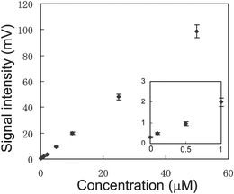 | ||
| Fig. 5 Calibration curve for investigating the LOD of the concentrations in the range of 0–25 µM. | ||
In this paper, the aluminum mirror was directly formed on the microchip surface by vacuum evaporation. Another plate with the aluminum mirror can also be utilized as a reflector, if the plate is attached to the microchip with fixing tools. In this case, just the single mirror plate is needed even if the microchips are replaced.
Conclusions
A reflective thermal lens detection device was developed for realizing a compact and sensitive detection device for microsystems. We realized high precision measurements by separation of a mirror from the microchannel and tilt angle regulations correction by a quadrant photodiode. For applications, we are now developing a point of care medical device with a portable thermal lens detection device and plastic microchips.17 Reagents for blood components analysis by colorimetric detection are established for single laser-diode excitation (wavelength of 635nm),17 the wavelength is suitable because of small interference from blood components. In addition, the selectivity can be realized by enzymatic reaction or immunoassay. We believe our microsystem will provide a powerful tool for various analytical fields.Acknowledgements
We gratefully acknowledge Prof. Takehiko Kitamori of The University of Tokyo for useful discussions and suggestions.References
- M. Gosch, H. Blom, J. Holm, T. Heino and R. Rigler, Anal. Chem., 2000, 72, 3260–3265 CrossRef.
- S. E. Bialkowski, Photothermal Spectroscopy Methods for Chemical Analysis, John Wiley & Sons, New York, 1996 Search PubMed.
- N. J. Dovichi and J. M. Harris, Anal. Chem., 1979, 51, 728–731 CrossRef CAS.
- N. J. Dovichi and J. M. Harris, Anal. Chem., 1980, 52, 2338–2342 CrossRef CAS.
- N. J. Dovichi and J. M. Harris, Anal. Chem., 1980, 52, 695A–706A CAS.
- N. J. Dovichi and J. M. Harris, Anal. Chem., 1981, 53, 689–692 CrossRef CAS.
- J. P. Haushalter and M. D. Morris, Appl. Spectrosc., 1980, 34, 445–447 CAS.
- K. J. Skogerboe and E. S. Yeung, Anal. Chem., 1986, 58, 1014–1048 CrossRef CAS.
- K. Uchiyama, A. Hibara, H. Kimura, T. Sawada and T. Kitamori, Jpn. J. Appl. Phys., 2000, 39, 5316–5322 CrossRef CAS.
- T. Kitamori, M. Tokeshi, A. Hibara and K. Sato, Anal. Chem., 2004, 76, 52A–60A CAS.
- M. Tokeshi, M. Uchida, A. Hibara, T. Sawada and T. Kitamori, Anal. Chem., 2001, 73, 2112–2116 CrossRef CAS.
- K. Mawatari, T. Kitamori and T. Sawada, Anal. Chem., 1998, 70, 5037–5041 CrossRef CAS.
- K. Sato, M. Tokeshi, T. Odake, H. Kimura, T. Ooi, M. Nakao and T. Kitamori, Anal. Chem., 2000, 72, 1144–1147 CrossRef CAS.
- M. Tokeshi, T. Minagawa, K. Uchiyama, A. Hibara, K. Sato, H. Hisamoto and T. Kitamori, Anal. Chem., 2002, 74, 1565–1571 CrossRef CAS.
- H. Hisamoto, T. Horiuchi, K. Uchiyama, M. Tokeshi, A. Hibara and T. Kitamori, Anal. Chem., 2001, 73, 5551–5556 CrossRef CAS.
- H. M. Sorouraddin, A. Hibara, M. A. Proskurnin and T. Kitamori, Anal. Sci., 2000, 16, 1033–1037 CAS.
- K. Shimoide, K. Mawatari, S. Mukaiyama and H. Fukui, in Proceedings of Micro Total Analysis System 2002, ed. Y. Baba, S. Shoji and A. van den Berg, Kluwer Academic Publishers, The Netherlands, 2002, pp. 918–921 Search PubMed.
- A. Hattori, H. Yamaguchi, J. Yamaguchi, Y. Matsuoka, S. Kanki, T. Fukuzawa, T. Miwa, M. Toyama, M. Tokeshi and T. Kitamori, in Proceedings of Micro Total Analysis System 2003, ed. M. A. Northrup, K. F. Jensen and D. J. Harrison, Kluwer Academic Publishers, The Netherlands, 2003, pp. 359–362 Search PubMed.
- M. Tokeshi, J. Yamaguchi, A. Hattori and T. Kitamori, Anal. Chem., 2005, 77, 626–630 CrossRef CAS.
- K. Mawatari, Y. Naganuma and K. Shimoide, Anal. Chem., 2005, 77, 687–792 CrossRef CAS.
- T. S. Wang, J. H. Aiken, C. W. Huie and R. A. Hartwick, Anal. Chem., 1991, 63, 1372–1376 CrossRef CAS.
Footnote |
| † Present address: Microchemical group, Kanagawa Academy of Science and Technology (KAST), Tokyo, Japan. |
| This journal is © The Royal Society of Chemistry 2006 |