Integrated microfluidic UV absorbance detector with attomol-level sensitivity for BSA
L.
Zhu
a,
C. S.
Lee
bc and
D. L.
DeVoe
*ac
aDepartment of Mechanical Engineering, University of Maryland, College Park, MD, USA
bDepartment of Chemistry and Biochemistry, and University of Maryland, College Park, MD, USA
cBioengineering Program, Don DeVoe, Department of Mechanical Engineering, University of Maryland, College Park, MD 20742, USA. E-mail: ddev@eng.umd.edu; Fax: +1 301-314-9477; Tel: +1 301-405-8125
First published on 3rd November 2005
Abstract
An integrated UV absorbance detection system employing a novel silicon-in-plastic technology to seamlessly integrate bare UV photodiode chips into polymer microfluidic systems has been developed. Detection platforms fabricated using this approach exhibit exceptionally low concentration and mass detection limits down to 15 nM and 9.8 amol, respectively, for bovine serum albumin (BSA) as a model protein. In addition to providing high sensitivity, sub-nanoliter detection volumes are enabled by the use of direct photodiode integration. The fabrication methodology is detailed, and system performance metrics including detection limits, detection volume, dynamic range, and linearity are reported.
Introduction
Due to its label-free nature and relatively simple implementation, absorbance detection remains the most prevalent method for the analysis of proteins in microscale capillary separations. Direct absorbance measurements in the near UV range are often used due to strong absorbance characteristics around 280 nm for several protein chromophores, in particular the aromatic ring amino acids Trp, Tyr, and Phe. Direct absorption measurements made perpendicular to the flow through silica capillaries with inner diameters below 100 µm typically yield detection limits on the order of 10−5 to 10−6 M.1 In order to improve measurement sensitivity, detection cells with longer pathlengths have been developed through the use of modified capillary geometries. However, as the path length increases, transmitted power decreases, eventually reducing the overall signal-to-noise ratio (SNR) as experimentally validated by Kutter et al.2 Furthermore, modified geometries providing longer optical pathlengths invariably lead to loss of effective separation resolution due to the larger minimum bandwidth defined by the optical pathlength,3 as well as the potential for band broadening introduced by geometric transitions between separation and detection volumes.The limitation imposed by reduced separation efficiency becomes critical for absorbance detection in microfluidic separation platforms, where minimum bandwidths of separated species tend to be on the order of several hundred microns. For example, an average bandwidth of 150 µm has been reported for proteins separated by gel electrophoresis in a 2.5 cm long polycarbonate (PC) microchannel.4 Thus, there is a need for techniques to realize improvements in SNR without sacrificing the ability to resolve the higher efficiency separations offered by microfluidic systems. To this end, several approaches have been explored. Integrated optical components have been widely reported for improved optical coupling efficiency within small-volume microfluidic flow cells. For detection, both in-plane5–7 and out-of-plane8 fiber optic waveguides coupled to off-chip optical detectors have been used for absorbance measurements in microfluidic chips. To provide a higher level of integration while avoiding difficulties with optical fiber alignment, monolithic waveguides have also been used for small volume microfluidic absorbance detection.2,9–11
Further improvements in integration have been realized by directly coupling planar photodetectors into microfluidic systems, thereby eliminating the optical losses and fabrication complexity associated with fiber optic or monolithic waveguides. Fully integrated, monolithic systems combining photodetectors and microchannels within a single silicon substrate have been demonstrated by several groups.12,13 These platforms enable the placement of an optical detection element immediately adjacent to the volume of analyte being imaged, thereby eliminating the need for focusing optics to improve the collection efficiency. However, a significant disadvantage of this monolithic approach is the high fabrication cost, which is likely to prevent its practical use in disposable bioanalytical tools. Related work has focused on a hybrid approach, with optical detectors fabricated in a first substrate, and microchannels fabricated in a second substrate and aligned to the optics prior to bonding or assembly of both layers.14–17 While this approach simplifies the overall fabrication to some extent, processing costs associated with the photodetector substrate remain a limitation. To further reduce cost, Adams et al. used a commercially available CMOS imaging chip as an optical detector substrate, with a small polydimethylsiloxane (PDMS) layer containing microfluidic channels aligned to the active side of the CMOS chip.18 While the maximum microchannel length used in this work was constrained by the small size of the CMOS chip, the concept of using an off-the-shelf silicon photodetector chip combined with a separate microfluidic substrate represents an intriguing solution for realizing low cost absorbance detection in a microfluidic platform.
In the present work, the idea of combining commercial silicon photodetectors with polymer microfluidics is extended using a new approach in which bare photodetector dies are seamlessly integrated into a larger polymer microfluidic substrate. Thus, rather than placing microfluidics atop a photodetector substrate, individual photodetector elements are placed within the polymer microfluidic substrate. This silicon-in-plastic approach offers several benefits. First, compared to previous demonstrations involving monolithic or hybrid integration of microchannels with custom-fabricated optical detection substrates, fabrication costs are lower. Since the cost per unit area for photodiode fabrication is significantly higher than for the microfluidic substrate, the ability to use no more than the necessary silicon area substantially reduces fabrication expense. Second, unlike previous demonstrations involving the placement of a microfluidic layer on top of a small silicon chip,18 the size of the microfluidic substrate is not limited when using the silicon-in-plastic approach.
Fabrication
Photodetectors
Silicon p-n junction photodiodes (UVG-series, International Radiation Detectors (IRD), Torrance CA) tuned for detection in the 160 to 600 nm wavelength range were purchased as bare dies approximately 1.6 mm × 1.6 mm in size. The typical spectral response of UVG-series photodiodes as reported by the manufacturer is shown in Fig. 1(a). Additional details of the photodiode fabrication and performance is available in the literature.19,20 Photodiodes with different active areas, namely (160 µm)2, (70 µm)2 and (25 µm)2, were used in this study. | ||
| Fig. 1 (a) The typical spectral response of UVG series photodiodes and (b) the normalized spectral response of the integrated UV absorbance detection system bonded with PDMS microchannel. | ||
Material selection
In addition to material properties required for effective mass production of polymer microfluidics using micromolding or embossing technologies, optical properties such as light transparency within the desired wavelength range are important characteristics. For peptide and protein detection, the chip material should ideally be transparent in the wavelength range of 214–280 nm. Rohr et al. summarized the UV-spectral of quartz, glass, and several commercial polymers.21 While quartz is transparent well into the deep-UV, most polymers are opaque below 300 nm, and are therefore not suitable for the present application. Among the available synthetic polymers commonly used for fabricating microfluidic systems, PDMS and cyclic olefin copolymer (COC) exhibit the best transparency between 220–300 nm. PDMS was used in the present study due to ease of fabrication. The normalized spectral response of an integrated photodiode together with a 2.1 mm thick layer of PDMS bonded to the detector surface is shown in Fig. 1(b). While PDMS is sufficiently transparent around 280 nm for effective protein detection, COC may be preferred for future development due to its optical clarity, excellent chemical resistance, good temperature stability, low water absorption, and low gas permeability.Silicon-in-plastic fabrication
The fabrication process developed for integration of bare photodetector chips into a polymer microfluidic substrate is shown in Fig. 2. The process is a modified version of a previously-reported procedure for seamlessly integrating silicon components into microfluidic systems.22 Briefly, a short wire is connected to the backside (anode contact) of the photodetector chip by conductive epoxy. A round mold hole large enough to accommodate the photodetector chip is milled through a polycarbonate (PC) substrate. The photodetector chip is temporarily placed face-down on a flat layer of cured PDMS (Sylgard 184; Dow Corning, Midland, MI), and the milled PC substrate is positioned over the chip with the chip located inside the milled mold hole. The PDMS provides for easy mold removal while also forming a seal against the surface of the chip. The assembly is placed in a vacuum chamber and the mold hole is filled with epoxy (353ND; Epoxy Technology, Billerica, MA). Casting in vacuum prevents air bubbles from being trapped at the edge of the chip, which appear as large pits when the mold is removed. Filling the mold under vacuum is accomplished by placing a syringe into the vacuum chamber with epoxy at the syringe tip positioned at the mold hole, and a defined volume of air at the back of the syringe. After the epoxy is cured for 12 h at room temperature, followed by 12 h at 50 °C, the PDMS is removed. The epoxy serves to secure the chip within the PC substrate, while leveling the chip face to within 1 µm of the PC surface.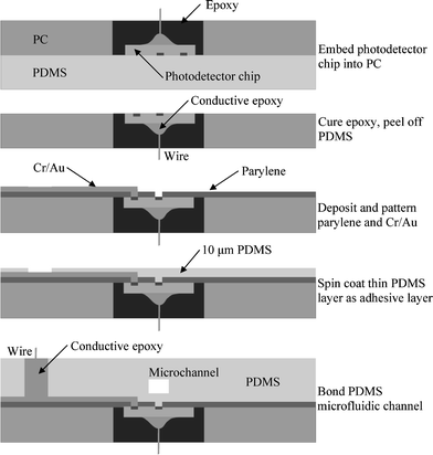 | ||
| Fig. 2 Fabrication process for the microfluidic absorbance detection platform. | ||
Although the epoxy layer can level the silicon chip surface to within 1 µm of the PC surface, small gaps can form at the silicon/epoxy/polycarbonate interfaces due to thermal mismatch and epoxy shrinkage during curing. These gaps, which are on the order of several microns deep, can cause several problems during the metal deposition process. First, the sidewall of the bare photodiode die is semiconducting silicon, and deposited metal which touches the sidewall can potentially shunt the active area contact to ground. Second, open circuits can form due to incomplete metal coverage over the gap. To overcome this problem, a ∼6 µm layer of parylene C is deposited to passivate the sidewalls and bridge small gaps prior to metal deposition. Parylene C covering the active area of the photodiode is removed by oxygen plasma etching using a Cr/Au mask. After the parylene layer is patterned, the mask metals are stripped, and new Cr (200 Å) and Au (5000 Å) layers are deposited and patterned to provide interconnections from the cathode contact on the photodiode to a connection pad on the PC substrate.
Next, a 10 µm thick layer of PDMS is spun onto the substrate and partially cured as an adhesive layer. The microfluidic channel was formed by micromolded PDMS from an SU-8 template. The PDMS layer was bonded to the substrate, with the active area of the photodetector located inside the microchannel using a microscope and manual aligner. After the PDMS structure was fully cured (50 °C for 8 h), conductive epoxy was applied to make contact to the cathode and anode interconnects. A photograph of completed device fabricated using this approach is shown in Fig. 3.
 | ||
| Fig. 3 Photograph of a fabricated microfluidic substrate with integrated photodetector chip. | ||
Experimental
A schematic of full test setup is shown in Fig. 4. Bovine serum albumin (66 kDa) was used as a model protein, with 10 mM Tris (hydroxymethyl) buffer was used to dilute protein sample. Both BSA and Tris buffer stock solutions were purchased from Sigma (St. Louis, MO). Diluted protein sample and Tris buffer were loaded into two syringe pumps (Harvard Apparatus, Holliston, MA), which were connected to the input reservoir of the microchannel through a capillary T connector and nanoport fitting (Upchurch Scientific, Oak Harbor, WA). A computer running MatLab was used to provide external control of the individual syringe pumps through an RS232 interface. | ||
| Fig. 4 (a) Schematic and (b) photograph of the testing apparatus used for data collection. The battery is used as a DC power supply to lower the photodetector noise floor. | ||
A commercial variable-wavelength ultraviolet absorbance detector with a deuterium lamp (Spectroflow 757; Applied Biosystems, Foster City, CA), was modified for use as the UV source. The standard flow cell was removed from the detector, and the microfluidic substrate was placed vertically on a 3D stage, with the integrated photodetector aligned with the UV output. The chip surface was positioned 6 mm from the terminal optics for the absorbance detector's UV output. Both the Spectroflow 757 and the 3D stage were fixed on a vibration isolation table to reduce noise. All testing was performed at 230 nm excitation in a dark room.
The small current signal generated by the integrated photodetector was amplified and converted to a voltage signal by a transimpedance amplifier interface. The voltage output data was captured using an Agilent data acquisition unit with a sampling rate of 1 s. The computer and data acquisition system were located outside the dark room to further reduce noise.
Before each experiment, the chip was flushed with Tris buffer for 10 min. Following warmup of the deuterium lamp for at least 5 min, Tris and BSA were alternately pumped through the channel for 10 min at a flow rate of 5 µL min−1. This cycle was repeated 3 times for BSA concentrations ranging from 0.001–1 mg mL−1, with a 10 min Tris buffer flush performed between changes in BSA concentration.
Results and discussion
Four devices with different photodetector chip sizes and different microchannel dimensions were fabricated and tested. Table 1 summarizes the design parameters for the four devices. In this table, the maximum detection volume is defined as the product of the channel width, channel depth, and PD width, and the minimum detection volume is defined as the product of the channel depth and the square of the PD width. While the minimum detection volume is the actual volume of the channel interrogated by the PD, the maximum detection volume accounts for portions of the channel width which are not interrogated, but which contain sample that would pass the detector during an actual separation. The limit of detection (LOD) for each design, set at 3 times the noise level and discussed in the following, are also given in the table. The mass LOD is specified as a range defined by the product of the concentration LOD and either the minimum or maximum detection volume. The upper limit of detection was constrained by protein precipitation, observed at concentrations above 50 mg mL−1. While not evaluated for each test, the dynamic range, given by the ratio of the predetermined precipitation limit to the concentration LOD, is also provided in Table 1.| Design 1 | Design 2 | Design 3 | Design 4 | ||
|---|---|---|---|---|---|
| Channel dimension | Width | 200 µm | 500 µm | 200 µm | 90 µm |
| Depth | 185 µm | 400 µm | 60 µm | 215 µm | |
| Active area of photodiode chip | (160 µm)2 | (70 µm)2 | (70 µm)2 | (25 µm)2 | |
| Detection volume | Minimum | 4.74 nL | 1.96 nL | 0.29 nL | 0.13 nL |
| Maximum | 5.92 nL | 14.0 nL | 0.84 nL | 0.48 nL | |
| Limit of detection BSA @ 230 nm | Concentration | 2 µg mL−1 (30.1 nM) | 1 µg mL−1 (15.2 nM) | 15 µg mL−1 (227.3 nM) | 5 µg mL−1 (75.8 nM) |
| Mass | 9.5–11.8 pg (144–179 amol) | 2.0–28.0 pg (30–212 amol) | 4.3–12.6 pg (66–191 amol) | 0.6–2.4 pg (9.8–36 amol) | |
| Dynamic range | 25![[thin space (1/6-em)]](https://www.rsc.org/images/entities/char_2009.gif) 000 000 |
50000 |
3300 | 10000 |
|
Fig. 5 exhibits the time-domain data traces showing normalized changes in measured absorbance for three analyte concentrations (BSA at 100, 10, and 1 µg mL−1) using chip design 2. As evident from this figure, BSA can be detected at 1 µg mL−1 (15.2 nM) using a photodiode chip with a 70 µm × 70 µm active area. This is substantially lower than the µM detection limits typically offered by capillary-based UV absorbance detectors with equivalent optical pathlengths.1,3 Furthermore, by reducing the detection volume using a photodetector chip with a smaller active area of 25 µm × 25 µm, a mass LOD as low as 9.8 amol (0.6 pg) was achieved (see Table 1). This detection limit is 2–3 orders of magnitude smaller than commercial UV absorbance detectors, and rivals many fluorescence-based detection methods which typically offer mass LODs on the order of 1–10 pg.
 | ||
| Fig. 5 Time-domain data traces showing changes in measured absorbance for three analyte concentrations (BSA at 100, 10, and 1 µg mL−1) using chip design 2 (see Table 1). The BSA solutions were pumped at 5 µL min−1, with flow switched on/off each 600 s. The data is normalized to the average baseline noise limit. | ||
The results of the BSA dilution measurements for each design are shown in Fig. 6. In this figure, the data points are average absorption measurements performed over 3 on/off cycles, with error bars reflecting ±1σ for each set of measurements. According to Lambert–Beer law, A = log(I0/I) = εcl, where A is the absorbance, I0 is the intensity of the incident light, I is the intensity of the transmitted light, ε is the analyte's molar extinction coefficient, l is the optical path length, and c is the analyte concentration.8 As can be seen from Fig. 6, all designs exhibit the expected linearity between absorbance and analyte concentration, with some deviation at low concentrations.
 | ||
| Fig. 6 Calibration curves for all tested chip designs. Data points are average absorption measurements performed over at least 3 on/off cycles, with error bars reflecting ±1σ for each set of measurements. | ||
Based on the Lambert–Beer relation, the sensitivity of the detection system can be increased linearly by increasing the optical path length. The four designs used in this study have different channel depths ranging from 60 µm to 400 µm. While designs with deeper channels generally offer lower detection limits, the relationship is not linear for several reasons. First, the terminal optics in the UV source are designed for focusing into a cylindrical flow cell rather than a planar chip, and thus the emitted light is not collimated. Second, the UV source spot size is larger than the active area of the photodetector chips, while at the same time the active area is smaller than the width of the microchannels, both by varying amounts depending on the specific design. Because of these factors, different amounts of optical scatter are expected from the four designs, thereby influencing the ultimate sensitivity of each detection system.
In commercial UV absorbance detectors designed for nanoscale liquid chromatography (nano-LC), UV is illuminated across the width of a capillary to achieve detection volumes in the low nL range. For the integrated microfluidic system, the photodetector is located directly against the microchannel, enabling exceptionally small detection volumes. Assuming an ideal case in which collimated light passes through the microchannel and optical dispersion may be neglected, the minimum detection volume is given by the product of channel height and active area of the photodetector. In practice, the UV illumination is not perfectly collimated, and optical dispersion and reflection from the channel surfaces may influence detection sensitivity. Reflections from the channel sidewalls are likely to be particularly significant. Thus, an upper limit on the maximum detection volume is given by the product of the channel height, channel width, and length of the photodetector active area. Both minimum and maximum detection volumes are provided in Table 1 for each design. In UV absorbance cells used for nano-LC, larger detection volumes generally imply lower spatial resolution due to longer path lengths along the axis of the capillary. For the integrated photodiode detectors, the spatial resolution is defined purely by the length of the active area oriented along the microchannel axis. This feature enables exceptionally high spatial resolution through the use of detectors with active areas as small as (25 µm)2. For maximum sensitivity and minimum detection volume, the ideal device would possess a deep and narrow microchannel, and a photodiode with an active area matched to the microchannel width.
Conclusion
The ability to integrate UV photodiodes into polymer microfluidic systems enables the fabrication of UV absorption detectors with sub-nL detection volumes and excellent detection limits on the order of 15 nM. Because the silicon-in-plastic technology allows photodiodes to be seamlessly combined with microfluidic channels with no interface gaps, the integrated detectors may potentially be used for monitoring protein separations without resolution loss due to sample dispersion when passing through the detection region. Furthermore, the low detection volume and high spatial resolution of the detectors is uniquely suited to effective monitoring of microfluidic separations. Further improvements in minimum detectible signal can be realized through the use of a differential measurement approach and improved interface electronics. With the emergence of low-cost silicon LEDs operating in the mid-UV range, it may also be possible to combine both excitation and detection in a fully integrated, low power analytical tool.Acknowledgements
This work was supported by NSF NIRT grant no. CTS0304318 and NIH grant no. GM072512.References
- Handbook of Capillary Electrophoresis, ed. J. P. Landers, CRC Press, New York, 1997 Search PubMed.
- D. Snakenborg, K. B. Mogensen and J. P. Kutter, Proc. Micro Total Analysis Systems, Squaw Valley, CA, 2003, pp. 841–844 Search PubMed.
- K. Swinney and D. J. Bornhop, Electrophoresis, 2000, 21, 1239–1250 CrossRef CAS.
- Y. Li, J. S. Buch, F. Rosenberger, D. L. DeVoe and C. S. Lee, Anal. Chem., 2004, 76, 742–748 CrossRef CAS.
- Z. Liang, N. H. Chiem, G. Oevirk, T. Tang, K. Fluri and D. J. Harrison, Anal. Chem., 1996, 68, 1040–1046 CrossRef.
- K. W. Ro, B. C. Shim, K. Lim and J. H. Hahn, Proc. Micro Total Analysis Systems, Monterey, CA, 2001, pp. 274–276 Search PubMed.
- G. Oevirk, E. Verpoorte, A. Manz, M. Grasserbauer and H. M. Widmer, Anal. Methods Instrum., 1995, 2, 74–82 Search PubMed.
- L. Ceriotti, K. Weible, N. F. de Rooij and E. Verpoorte, Microelectron. Eng., 2003, 67, 865–871 CrossRef.
- K. B. Mogensen, N. J. Petersen, J. Hübner and J. P. Kutter, Electrophoresis, 2001, 22, 3930–3938 CrossRef CAS.
- N. J. Petersen, K. B. Mogensen and J. P. Kutter, Electrophoresis, 2002, 23, 3528–3536 CrossRef CAS.
- K. B. Mogensen, J. El-Ali, A. Wolff and J. P. Kutter, Appl. Opt., 2003, 42, 4072–4079 CrossRef CAS.
- A. M. Jorgensen, K. B. Mogensen, J. P. Kutter and O. Geschke, Sens. Actuators, B, 2003, 90, 15–21 CrossRef.
- V. Namasivayam, R. Lin, B. Johnson, S. Brahmasandra, Z. Razzacki, D. T. Burns and M. A. Burns, J. Micromech. Microeng., 2004, 14, 81–90 CrossRef CAS.
- I. Rech, A. Restelli, S. Cova, M. Ghioni, M. Chiari and M. Cretich, Sens. Actuators, B, 2004, 100, 158–162 CrossRef.
- G. Minas, J. Martins, J. Ribeiro, R. Wolfenbuttel and J. Correia, Sens. Actuators, A, 2004, 110, 33–38 CrossRef.
- T. Kamai, B. M. Paegel, J. R. Scherer, A. M. Skelley, R. A. Street and R. A. Mathies, Anal. Chem., 2003, 75, 5300–5305 CrossRef CAS.
- O. Leistiko and P. Friis, Proc. SPIE-Int. Soc. Opt. Eng., 1999, 3606, 10–19 CAS.
- M. L. Adams, M. Enzelberger, S. Quake and A. Scherer, Sens. Actuators, A, 2003, 104, 25–31 CrossRef.
- R. Korde, C. Prince, D. Cunningham, R. E. Vest and E. Gullikson, Metrologia, 2003, 40, 145–149 Search PubMed.
- L. R. Canfield, R. E. Vest, R. Korde, H. Schmidtke and R. Desor, Metrologia, 1998, 35, 329–334 Search PubMed.
- T. Rohr, D. Frank Ogletree, F. Svec and J. M. J. Frechet, Adv. Funct. Mater., 2003, 13, 264–270 CrossRef CAS.
- L. Zhu, C. Kimball, N. Sniadecki, S. Semancik and D. L. DeVoe, Proc. MicroTAS 2003, Squaw Valley, CA, Oct. 5–9, 2003, pp. 1231–1234 Search PubMed.
- R. D. Tacito and C. Steinbruchel, J. Electrochem. Soc., 1996, 143, 1974–1977 CAS.
| This journal is © The Royal Society of Chemistry 2006 |