Nano-chemistry and scanning probe nanolithographies
Ricardo Garcia, Ramses V. Martinez and Javier Martinez
Instituto de Microelectrónica de Madrid, CSIC, Isaac Newton 8, 28760 Tres Cantos, Madrid, Spain. E-mail: rgarcia@imm.cnm.csic.es
First published on 21st November 2005
Abstract
The development of nanometer-scale lithographies is the focus of an intense research activity because progress on nanotechnology depends on the capability to fabricate, position and interconnect nanometer-scale structures. The unique imaging and manipulation properties of atomic force microscopes have prompted the emergence of several scanning probe-based nanolithographies. In this tutorial review we present the most promising probe-based nanolithographies that are based on the spatial confinement of a chemical reaction within a nanometer-size region of the sample surface. The potential of local chemical nanolithography in nanometer-scale science and technology is illustrated by describing a range of applications such as the fabrication of conjugated molecular wires, optical microlenses, complex quantum devices or tailored chemical surfaces for controlling biorecognition processes.
 Ricardo García | Ricardo García (1960) is a Professor of scientific research at the Instituto de Microelectrónica de Madrid (CSIC). He received Graduate and Master degrees in Physics from the Universidad de Valladolid in 1983 and 1984, respectively. In 1984 he moved to the Universidad Autónoma de Madrid to join the group of Prof. Nicolás García. He received a PhD degree in Physics (March 1990), for theoretical studies on electron tunneling in metals, insulators and biomolecules, and scanning tunneling microscopy imaging. He worked with Prof. Carlos Bustamante as a postdoctoral associate, first at the University of New Mexico and later at the Institute of Molecular Biology (University of Oregon) (1990–1993). His postdoctoral research involved the development of scanning tunneling microscopes to study biomolecules (DNA, protein membranes) and biomolecular interactions. Garcia's research emphasizes two topics, the development of novel scanning probe-based nanolithographies and the development of multipurpose tools for quantitative analysis and manipulation of molecules, materials and devices in the 1 to 100 nm length scale. Prof. García is an editorial board member of the Review of Scientific Instruments. |
 Ramsés V. Martínez | Ramsés V. Martínez was born in Madrid in 1981. He received a degree in physics from the Universidad Autónoma de Madrid in June 2004. He then entered the PhD program at the UAM under the direction of Prof. R. García. His current research focuses on the development of scanning probe nanolithographies based on the spatial confinement of chemical reactions within a liquid meniscus. |
 Javier Martinez | Javier Martinez (Valladolid, Spain, 1973) is a postdoctoral researcher in the group of Prof. Garcia at the Instituto de Microelectronica in Madrid. After working on electronic sensors during his PhD studies at the Universidad de Valladolid, he joined Prof. Carlos Bustamante's group as a postdoctoral associate (University of California, Berkeley) where he was involved in the fabrication of carbon nanotube AFM tips. He rejoined the Garcia group in 2005. His current interests include parallel local oxidation and ultra high resolution of biological systems with scanning probe methods. |
Introduction
The emergence of nanoscience and nanotechnology depends, at least partially, on the ability to position, manipulate and fabricate a variety of structures, materials and devices with accuracy in the nanometer-scale. It also rests on the incorporation of organic and biological molecules as active components of mechanical, electrical or molecular recognition devices. Furthermore, for progress to be made in this area it is necessary to understand the underlying science and engineering involving nanoscale structures and devices, which experimentally requires, among other things, the development of accessible, flexible and robust nanofabrication approaches. Conventional nanolithographies, i.e., those derived from optical and electron beam lithographies are either cost-intensive or unsuitable to handle the large variety of organic and biological systems available in nanotechnology. The above driving forces have stimulated the development of alternative nanofabrication techniques. This process started approximately in 1990 and it has given rise to the establishment of three major nanolithography methods: nano-imprint lithography, soft lithography and scanning probe-based nanolithographies.1–3Scanning probe microscopes, in particular atomic force microscopes (AFM), enjoy a prominent status in nanotechnology because of their ability to image at sub-10 nm resolution a wide variety of surfaces ranging from biomolecules to integrated circuits. Furthermore, the performance of the instrument is not compromised by the medium. High resolution imaging has been achieved in air, liquids or vacuum. The relative ease of conversion of a force microscope into a modification tool has prompted a fascinating variety of atomic and nanometer-scale modification approaches. Those approaches involve the interaction of a sharp probe with a local region of the sample surface. Mechanical, thermal, electrostatic and chemical interactions, or several combinations among them, are currently exploited to modify surfaces at the nanoscale with probe microscopes (Fig. 1).4–10
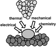 | ||
| Fig. 1 Scheme of some common mechanisms to modify surfaces with scanning probe nanolithographies. | ||
The proposed approaches range from the sophisticated monitoring of attractive van der Waals forces to control atoms to the crude approach of scratching surfaces by ploughing a nanometer-sized tip; from the selective oxidation of a metallic surface to fabricate quantum devices to the thermo-plastic deformation of polymers to fabricate flash memories. However, just a few of the proposed approaches are suitable for large scale and reproducible patterning of materials. In most cases, technical requirements such as the use of ultra high vacuum and low temperatures have rendered many of these methods of little practical relevance.
Among the most successful scanning probe nanolithographies (SPL) are those based on the spatial confinement of a chemical reaction within a nanometer-size region. The region is usually defined by either a combination of the probe-sample surface geometry or the combination of the geometry and another factor that could be an external electrical field or a liquid meniscus. In particular nanometer-size water meniscus11 have appeared as remarkable tools to either confine the lateral extension of a chemical reaction or to control the lateral diffusion of organic molecules. Given the meniscus nanoscale size, nanofabrication and nanochemistry are intimately linked in the SPL methods reviewed here.
This tutorial review aims to provide an overview of scanning probe nanolithography methods where the nanofabrication process is mediated by a local chemical reaction. In particular we discuss local oxidation nanolithography10–12 and its generalization through the use of polar and non-polar liquids as well as other emerging methods such as dip-pen nanolithography13 and chemomechanical patterning.14 Those methods allow exploration of the relationship existing between nanolithography and nanochemistry. They could be integrated under the name of local chemical nanolithographies. Some of the probe-based methods are still in their infancy, i.e., the emphasis is placed on the (nano)patterning of a given region of the sample surface while others such as local oxidation have reached a higher level where fabrication and device performance are strongly emphasized. Nonetheless, all of them are in a strong development stage.
In general, local chemical nanolithographies offer to the academic researcher a low-cost and versatile alternative to fabricate and investigate the properties of a large variety of organic and inorganic structures, and devices at the nano-scale. The flexibility to handle organic, biological and inorganic surfaces alike provided by local chemical nanolithographies may explain their growing acceptance in the nanoscience and nanotechnology community. Fig. 2 shows some common experimental set-up elements of SPL.
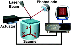 | ||
| Fig. 2 Main elements of an AFM dedicated to nanolithography. | ||
Local oxidation nanolithography
Since the inauspicious discovery of scanning probe-based oxidation12 in the heyday of atomic-scale manipulation of surface by scanning tunnelling microscopy (STM), local oxidation nanolithography has evolved to become a useful tool to fabricate sophisticated devices for studying a variety of quantum phenomena such as coulomb blockade, quantum conductance and the like. In 1990 Dagata and co-workers modified a hydrogen-terminated silicon surface by the application of a bias voltage between an STM tip and the surface.12 Secondary ion mass spectroscopy showed the presence of silicon oxide in the modified regions. In 1993 it was demonstrated that local oxidation experiments could be performed with an atomic force microscope.16 This observation paved the way for the development and expansion of local oxidation approaches to modify surfaces. The versatility of the method together with the astonishing variety of materials amenable for anodic oxidation explains the wide use of this scanning probe-based nanolithography. Local oxidation nanolithography (LON) is sometimes called scanning probe oxidation, nano-oxidation, local anodic oxidation or generically AFM lithography.The present knowledge allows some similarities between local oxidation and conventional anodic oxidation to be established. The AFM tip is used as a cathode and the water meniscus formed between tip and surface provides the electrolyte (Fig. 3). The meniscus is usually induced by the application of an electrical field, although in some cases it can also be driven by the mechanical contact between tip and sample surface. The end result is the formation of a nanometer-size electrochemical cell (nanocell) that contains about 5 × 10⁴ molecules. The method to form liquid bridges is so precise that water meniscus diameters of 20 nm are easily obtained. This has lead to the reproducible fabrication of sub-10 nm structures in Si and even smaller structures in titanium films.
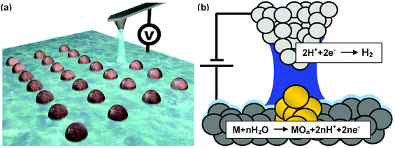 | ||
| Fig. 3 (a) Schematics of a local oxidation nanolithography experiment. The meniscus provides the oxyanions and confines the spatial extent of the reaction. (b) Accepted chemical reactions in the local oxidation of a metallic surface. | ||
Local oxidation experiments were first performed on Si(111) and polycrystalline tantalum faces. Since then a large number of materials have been locally oxidized such as compound III–V semiconductors, silicon carbide, several metals such as titanium, tantalum, aluminium, molybdenum, nickel and niobium; perovskite manganite thin films, dielectrics such as silicon nitride films as well as organosilane self assembled monolayers, dendritic objects and carbonaceous films.
Silicon faces either with or without hydrogen passivation have been thoroughly modified by LON. They serve as a good model to illustrate some of the fundamental aspects involved in the local oxidation process.16–19 Voltage pulses are applied to generate an oxide dot. The dot size depends linearly on voltage strength but the dot height shows a power law dependence of the type
| h ∼ (t/t0)γ | (1) |
The local oxidation process is accompanied by an extremely small current.17,20 The value depends on the final dot size. Common values are in the sub-picoampere regime. Experimental observations have shown that the current through the interface during oxidation matched the current calculated from the measured oxide volume by taken into account that four elementary charges are needed to oxidize one Si atom. This observation together with the presence of a water meniscus points out the electrochemical nature of the process.
For silicon, the reactions in the nanocell are described by the following half-cell reactions. In the anode (sample surface) the oxidation takes place according to
| Si + 2h+ + 2(OH−) → Si(OH)2 → SiO2 + 2H+ + 2e− | (2) |
While hydrogen generation occurs at cathode to complete the electrochemical reaction
| 2H+(aq) + 2e− → H2 | (3) |
For a metallic surface the following half-cell reaction (anode) has been proposed,
| M + nH2O → MOn + 2nH+ + 2ne− | (4) |
Photoemission spectroscopy on Si and GaAs have confirmed that indeed the chemical composition of the fabricated structures were silicon and gallium arsenide oxides respectively.21 Usually heights are measured with respect to the substrate baseline, consequently reported oxide heights differs from the true oxide thickness. In Si approximately 60% of the oxide is above the substrate baseline.
A feature that distinguishes local oxidation nanolithography from other scanning probe-based modification methods is that modification and imaging processes operate independently. Long range van der Waals forces and/or short range repulsive forces are used to image the surface while an external voltage is applied to induce the local oxidation of the surface. Another relevant feature is that it allows in situ control of the device electrical and topographic characteristics during its fabrication.
Local oxidation processes allow the direct fabrication of three elements, dielectric barriers, masks for selective etching and templates. The combination of those elements allows the fabrication of a wide range of electronic and mechanical devices with nanometer-scale features.22–29 In some cases LON is used in combination with other methods such as photolithography, electron beam lithography or chemical wet etching to fabricate the desired device. In those cases, the critical or most relevant features of the device are fabricated by local oxidation. The list of devices fabricated by LON is quite large, it includes data storage memories, conducting nanowires, side-gated field-effect transistors, single electron transistors, superconducting quantum interference devices, quantum points and rings, microlens, templates for the growth of biomolecules and conjugated materials and etch resistant masks.
The flexibility of LON to pattern arbitrarily shaped patterns is illustrated in Fig. 4. Alternating insulating and semiconducting rings, arrays of dots and the first ten lines of ‘Don Quixote’ have been written by local oxidation.
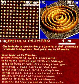 | ||
| Fig. 4 Examples of local oxidation nanopatterns. (a) Periodic array of 10 nm silicon oxide dots. The lattice spacing is 40 nm. (b) Alternating insulating (bright) and semiconducting rings. (c) First paragraph of ‘Don Quixote’. | ||
Although one of the strengths of LON resides in the unique imaging and positioning properties of AFM, recent experiments have demonstrated that the fundamental physical and chemical processes governing local oxidation are scalable. Millimeter square regions have been patterned in a few seconds by using stamps with millions of nanometer-size protrusions, each of them acting as single AFM tip.31,32 Those experiments open new routes for bridging nano and macroscale devices.
Memories, optical microlens and quantum devices
It is relatively straightforward to apply local oxidation nanolithography to pattern arrays of dots that could serve as read-only memories. In particular Fig. 4a shows an array of dots with a lattice spacing 40 nm. If each dot is identify as ‘1’ and the absence of dot as ‘0’ the areal density of the pattern is 400 Gbits in−2. By using single-wall carbon nanotube probes and Ti films, Quate and co-workers22 in 1999 demonstrated an areal density of 1.6 Tbits in−2. They patterned dots with a lattice spacing of 20 nm. We have slightly increased the above areal density by patterning interdigitated arrays of silicon oxide lines24 with a lattice spacing down to 13 nm. Although areal densities of magnetic hard disks are about two orders of magnitude smaller (state-of-the-art hard disk drives have areal densities of about 10 Gbits in−2), the written rate reached in LON (∼5 Kbit s−1) and the permanent character of oxide dots (bits) severely limit the applications for data storage. Fig. 5 shows a series of interdigitated silicon oxide lines with a length of 400 nm and a lattice periodicity of 19.5 nm.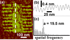 | ||
| Fig. 5 (a) Set of 18 interdigitated silicon oxide lines fabricated by LON. (b) Cross-section along the dashed line in (a). (c). The Fourier transform of (b) reveals a periodicity of 19.5 nm. The lines were obtained by applying pulses of 21 V and 80 µs (from ref. 24). | ||
To illustrate the degree of sophistication achieved by LON to fabricate functional nanoelectronic and micromechanical devices we will describe the fabrication process of three devices: silicon microlenses, metal-oxide tunnelling transistors and quantum rings.
One of the first nanoelectronic devices operating at room temperature was fabricated by using local oxidation nanolithography. In 1995 Snow and co-workers established the foundations to fabricate very thin tunnelling barriers by local oxidation and to use them to make transistors. This process was applied to fabricate a 30 nm-wide lateral NbOx tunnel barrier separating two Nb electrodes. The electrodes were placed on top of an insulating film (Al2O3) with a buried gate. The transistor operates by using a gate field to modulate the transmission of electrons through a lateral/metal oxide barrier. The gate electrical field either increase (decrease) the height of the tunnel which in turns increases (decreases) the current flowing between the electrodes.29
Several complex quantum mechanical devices have been fabricated by Ensslin and co-workers.30 For example, they have fabricated a quantum ring on a semiconductor heterostructure (AlGaAs/GaAs) containing a two-dimensional electron gas. The oxidation produces the depletion of the electron gas underneath, which in turns, transforms a conducting region into an insulating region. Local oxidation has been used to carve the ring as well as the quantum point contacts. The current passes from source to drain and different gates are used to tune the quantum point contacts (qpc1a, qpc1b, qpc2a, qpc2b) and the current flowing through the ring (pg1 and pg2) (Fig. 6). After the oxidation the sample has been covered by a metallic electrode and tuned into the Coulomb blockade regime.
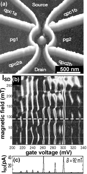 | ||
| Fig. 6 (a) AFM image of a quantum ring fabricated by LON. The oxide lines (bright regions) depleted the two dimensional electron gas 34 nm below the surface separating the sample into several conductive regions. The in-plane gates qpc and pg are used to tune the point contacts and the two arms of the ring. (b). Evolution of the current as a function of the magnetic field and the gate voltages (pg1 and pg2). The Aharanov–Bohm period expected from the ring geometry is indicated by the thin horizontal lines. (c) Coulomb blockade resonances at fixed magnetic field (adapted from ref. 30). | ||
The current through the ring as a function of the gate voltage and the magnetic field is plotted in Fig. 6b, while the Coulomb blockade oscillations at a fixed magnetic field can be appreciated in Fig. 6c. From this plot the charging energy can be measured as Ec = e2/CΣ ≈ 190 µeV, CΣ being the total capacitance of the ring.
Gwo and co-workers have succeeded in performing quite sophisticated micromachining by LON. Very recently they have combined local oxidation and dry anisotropic etching to fabricate convex, concave and arbitrarily shaped silicon microlenses with diameters of 2 µm and a focal length of 4 µm, i.e., about one order of magnitude smaller than the ones obtained with standard techniques by using photolithography. Furthermore, Gwo's approach has the potential to fabricate lenses with a pixel size of 10 nm. Some examples of the spherical and circular silicon microlenses fabricated by local oxidation are illustrated in Fig. 7.
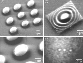 | ||
| Fig. 7 Scanning electron microscopy images of several Si microlenses fabricated by LON. (a) Array of 9 microlenses. The lenses are of 2 µm diameter. (b) Circular Si microlenses. (c) Infrared optical image taken at the focal plane of a 1 × 3 microlens array. The diameter of each lens is 8 µm (from ref. 28). | ||
Nanopatterning of self-assembled monolayers
Self-assembly, chemical functionality and nanopatterning are concepts very akin to nanotechnology, so it is not surprising to discover various approaches to modify self-assembled monolayers or to induce a selective self assembly process by LON.33–36 Sugimura and co-workers pioneered the protocol to generated coplanar nanostructures consisting of two different types of self-assembled monolayers (SAM).33 The two step process is illustrated by describing the generation of coplanar alkyl monolayers. The first monolayer is self-assembled on a hydrogen passivated silicon surface. Then local oxidation is performed on a selected spot of the monolayer. The oxidation removes the SAM underneath the tip. The modified region is probably terminated in OH groups, so it is ready to react with different organosilane molecules while the unmodified regions are unreactive. In the second step, the sample is immersed in a solution containing octadecyltrichorosilane (OTS). Those molecules will react with the oxidized regions which gives rise to the formation of a new self-assembled monolayer. The process admits several variations, for example, if the second organosilane has terminal amino groups, those groups could be used to bind negatively charged particles or molecules.Sagiv and co-workers have developed a highly sophisticated approach to modify self-assembled monolayers by LON. In their approach,35,36 they start initially with an OTS monolayer on silicon. Then the applied voltage is tuned in such a way to oxidize the terminal groups of the first monolayer by converting the methyl groups into carboxylic groups. In the next step, a NTS (nonadecenyltrichlorosilane) treatment follows to attach another monolayer with terminal –CH![[double bond, length as m-dash]](https://www.rsc.org/images/entities/char_e001.gif) CH2 groups on the modified parts. This generates a second highly ordered monolayer with chemically reactive terminal ethylenic functions. A further chemical treatment that involves the induced photo reaction of H2S with the ethylenic groups produces a thiol terminated layer. The process allows the construction of locally multiple self-assembled monolayers (Fig. 8).
CH2 groups on the modified parts. This generates a second highly ordered monolayer with chemically reactive terminal ethylenic functions. A further chemical treatment that involves the induced photo reaction of H2S with the ethylenic groups produces a thiol terminated layer. The process allows the construction of locally multiple self-assembled monolayers (Fig. 8).
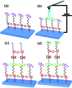 | ||
| Fig. 8 Scheme of the hierarchical self-assembled approach developed by Sagiv et al. (ref. 35). (a) SAM on Si substrate. (b) Patterned SAM by local oxidation of methyl terminated groups. (c) and (d) Different steps in the formation of a second monolayer in the patterned region. The transformation of the vinyl-terminated overlayer in amino-terminated requires the reaction of NTS groups with formamide and its further reduction with BH3.THF. | ||
Template growth of organic and biological structures onto nanopatterns
Developing methods that allow the deposition of small functional molecules at pre-determined positions on a substrate is one of the exciting challenges for alternative nanolithographies. In this section we illustrate the potential of LON in this topic by describing three applications, fabrication of gold patterns and nanowires onto SAM templates, patterning of proteins (ferritin) and fabrication of conjugated molecular tracks and nanowires.Nanopatterned self-assembly monolayers by LON offers a straightforward approach to introduce chemical functionality at the nanoscale and this can be exploited for the fabrication of several nanostructures such as electrodes and nanowires. To fabricate the gold wires and electrodes, Sagiv et al. immersed the modified SAM as described in Fig. 8 in a solution containing gold clusters36 (Au55). The gold clusters are attached to the thiol groups leaving the gold pattern in the regions previously modified with the AFM. The scheme of the process as well as some of the patterned gold motives can be seen in Fig. 9. In Fig. 9c a gold nanowire connected to an electrode has been patterned. In spite of the elegance of the approach, the electrical characteristics of those wires remains to be tested, so their usefulness as wires for electron transport is still unknown.
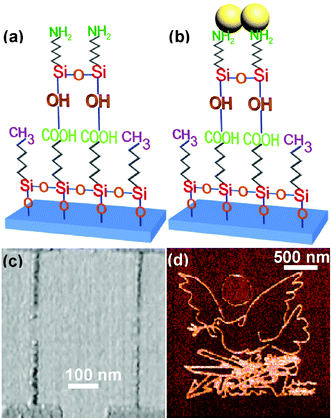 | ||
| Fig. 9 Template-guided self-assembly of gold nanoparticles on a organosilane bilayer template fabricated according to the scheme of Fig. 8. (a) Template bilayer. (b) Deposition of water-soluble (Au-citrate) colloidal particles on amino-terminated template patterns. (c) Fabrication of gold electrodes and wires. (d) Patterning of a Picasso drawing. The patterning was carried out with a 800 × 800 raster-scanned points at 3.3 ms per point and by applying a tip-surface voltage of 8.5 V (from refs. 35 and 36). | ||
Several protocols have been implemented for the template growth of proteins onto local silicon oxide templates.37 There the nanopatterns were used both as positive and negative templates, i.e., molecules deposited preferentially inside (positive) or outside (negative) the patterned motives. The method requires first the formation of a thin oxide layer on the silicon surface. This is accomplished by wet-chemical etching. This step is followed by a treatment with (OTS) which produces an alkyl monolayer. Then local oxidation removes the alkyl monolayer in a selected area. A subsequent exposure to a second silane (γ-APTES) produces a proteinphilic region on the local oxide that is the source of preferential interactions with the proteins.
Conjugated molecular materials are some of the basic components of most planar devices in plastic electronics which are on the micron scale. Conjugated molecular wires with nanometer size features have been fabricated by a process which is based on the integration of local oxidation nanolithography of the substrate and template growth of the molecular thin film by high-vacuum sublimation on the fabricated pattern. Local oxidation is used to fabricate silicon templates made of either parallel lines or stripes.38
Template growth of sexithiophene (T6) arises from the interplay between kinetics of growth and the preferential interactions with the patterned structures. The kinetic parameters allow the molecules to follow the contours of the growing island until they reach the silicon oxide line. The trapped charges within the local oxide generate a weakly screened long range electrostatic potential, that becomes especially relevant in the case of T6 because of its large anisotropic polarizability together with the inhomogeneous charge density distribution along the thiophene chain. This is the source of preferential, albeit not specific, interactions. The result is a monolayer film of organic molecules that conformally mimicks the features of the fabricated motives. Outside the patterned area the islands exhibit a morphology characterized by the presence of branches and fingers with no preferential orientation while the molecules grow preferentially on top of the stripes and parallel to them (Fig. 10). Tracks or wires of 6 µm in length with narrow channels below 100 nm in width have been fabricated with this method (Fig. 10b).
 | ||
| Fig. 10 AFM images of T6 molecules grown on a parallel set of local oxide stripes. The interaction of the T6 and the oxide lines gives rise to the anysotropic growth of the molecules. Formation of a T6 wire of 6 µm in length and 400 nm in width (average value) (adapted from ref. 38). | ||
Local chemical nanolithography
At this point it seems rather straightforward to pose oneself the question of what would happen if other liquids are used. Would it be possible to form reproducible patterns on the sample surface? Would it be possible to change the chemical composition of the formed structures? Tello and Garcia have performed modification experiments with polarizable organic solvents such as ethyl and propyl alcohols. In the case of the experiments performed with ethanol menisci, photoemission spectroscopy analysis revealed that the fabricated structures on a silicon surface were no longer oxides but showed the formation of silicon carbide and carbon sp2 compounds.39Frechet and co-workers have shown that operating the AFM in a liquid cell filled with n-octane gave rise to the formation of nanostructures that could be used as etch resistant resists.40 Because the fabricated structures were not etched by HF, it was concluded that those structures were not silicon oxides. However, experiments performed in other non-polar organic solvents such as hexadecane41 and 1-octene42 gave rise to structures that showed chemical and kinetic behaviour consistent with field induced oxidation in air. The above experiments reveal that on the same substrate (Si) the composition of the fabricated structure is organic solvent dependent.
Another interesting experiment that emphasized the electrochemical character of the modification process was performed by Li and co-workers.43 A silicon tip was coated with a water-soluble metal salt. The formation of a water meniscus dissolves some little amount of salts. When a positive voltage is applied, the metal ions dissolved in the water meniscus are reduced and deposited as a metal particles on the cathode. The method was applied to form Au, Ge, Ag, Cu and Pd structures.
Successful AFM modification experiments have also been performed in inert atmosphere to avoid water meniscus formation. For example, the localized chemical activation of a protected amine surface by the application of a voltage bias between the AFM and the silicon substrate has been reported.44
All the above experiments were performed with rather similar experimental set ups, i.e., an AFM with a voltage biased tip-sample interface enclosed in an environment control chamber. Consequently, the different modification methods discussed so far could be considered variations of a single probe nanolithography based on the spatial confinement and field-induced generation of chemical reactions. The spatial confinement could be achieved either by the formation of a liquid meniscus (nanocell) or by focusing the electrical field lines underneath the tip. In this context it fits to describe all of the above methods under the single term of local chemical nanolithography.
Dip-pen nanolithography
In 1995 Jaschke and Butt reported the deposition of organic molecules (octadecanethiols) from an AFM tip onto a mica surface.45 This process was rediscovered and developed for nanopatterning purposes by Mirkin and co-workers.46,14 The method was called Dip-pen nanolithography (DPN). In DPN inks are first adsorbed on the tip of an AFM, then transferred by diffusion to a pre-selected position of the substrate. The first DPN experiment was demonstrated by patterning alkanethiol self-assembled monolayers onto gold surfaces. The combination of the flexible terminal group chemistry given by alkylthiols and the AFM nanoscale control over physical dimensions explains the remarkable expectations raised by dip-pen nanolithography. The DPN approach is illustrated in Fig. 11.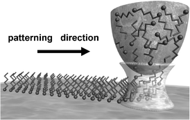 | ||
| Fig. 11 Scheme of the dip-pen nanolithography ink deposition. | ||
Some proteins and DNA molecules are amenable for thiol functionalization, thus they are also suitable for DPN. Patterns of DNA have been written on gold surfaces using hexanethiol-modified nucleotides. Furthermore, the resulting patterns were hybridized to DNA-functionalized gold nanoparticles. Proteins patterns have also been formed by DPN either by using thiolate proteins or by direct deposition of proteins on pre-prepared glass surfaces. The array of retronectin proteins depicted in Fig. 12 shows potential of DPN for studying and controlling biorecognition processes.
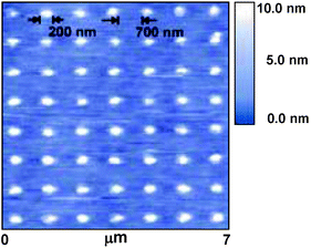 | ||
| Fig. 12 AFM image of a retronectin protein array patterned by DPN (from ref. 14) | ||
Until now few substrates have been suitable for DPN, they include gold, silicon, silicon oxide and glass, however, the list of inks successfully deposited by DPN is growing. They include alkylthioles, organosilanes, proteins, DNA, organic dyes, dendrimers and sols among others.14,47,48 The minimum feature size achieved by dip-pen is 15 nm for alkathiols inks on single-crystal gold surfaces.
The fundamental processes governing the transfer of organic molecules from the tip to the sample surface are still under debate. Mirkin et al. hypothesized that the diffusion process was mediated by the presence of a water meniscus. The formation of a water meniscus is an unavoidable fact in contact AFM operation in ambient conditions. However, other authors have argued that hydrocarbons are essentially insoluble molecules in water, so it seems unlikely that they could be transferred via the water meniscus.49 Furthermore, they succeeded in performing DPN experiments with octadecanethiol molecules on gold surfaces at 0% relative humidity.
A remarkable observation of the diffusion process is that all the deposited molecules obey the same functional form with respect to the time, area = kt + b, where k depends on ink, temperature and in some cases humidity while b reflects the tip size/coating dependence. The above expression underlines some of the limitations of DPN. For practical reasons, imaging and deposition are performed with the same tip, thus inked tips inherently cause contamination on the surface. Another limitation is the little control of deposition rate once the molecules have been adsorbed on the tip.
Dip-pen nanolithography has also been performed with arrays of cantilevers which opens the possibility for high-throughput parallel approaches.
Chemomechanical patterning
Exerting mechanical forces by the tip is the most intuitive approach to modify a surface by an AFM. Consequently in the late 80s and early 90s many research groups reported results on scratching surfaces by AFM. However, most of those approaches have been abandoned because of poor reproducibility and tip degradation. Usually the tip is irreversible damaged (blunted) after a few modifications. Nonetheless, several groups have recently revisited this approach to patterning of surfaces.15,50–52 The renewed interest in using mechanical forces comes from a combination of factors. On one side, state-of-the-art AFM technology allows the modulation of forces with nN accuracy. On the other side, the use of soft layers such as self-assembled alkyl thiol monolayers as sacrificial layers allows material removal without tip degradation. Usually mechanical removal is accompanied by the deposition of selected molecules that form covalent bonds with the exposed surface, termed chemomechanical patterning.Chemomechanical patterning has the following experimental protocol. First, it requires the definition of two range of forces. Low forces, say of about 1 nN for imaging and high forces, say of about 10–50 nN for modification. Each sample has its set of threshold values. The surface to be modified either a self-assembled monolayer or a rigid substrate and the AFM tip are immersed in a fluid cell. At low forces the AFM images the surface. By increasing the force above a certain threshold, the SAM becomes disordered and adsorbates are displaced leaving the bare substrate. This is usually called nanoshaving. If the removal of the sacrificial SAM is done in the presence of another molecule solution with a higher concentration than the displaced SAM, the new molecules will be grafted onto the substrate surface. High-density alternating nanostructures of octodecanethiol and decanethiol with a periodicity of 14 nm have been fabricated on gold surfaces.50 If the shaving of the SAM is performed in a solution containing gold nanoparticles, the nanoparticles then adsorb onto the exposed areas50. Deposition of organic molecules such as 1-hexadecane or 1-octanol have been obtained in hydrogen-terminated silicon (111) surface.52
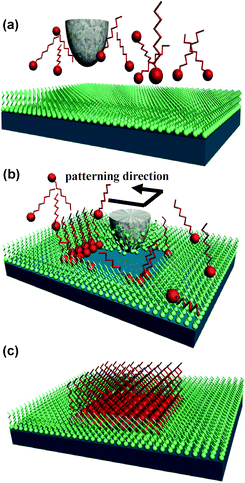 | ||
| Fig. 13 Scheme of chemomechanical patterning. (a) A SAM is assembled on the surface. (b) The AFM tip exerts a force on the SAM and removes the monolayer in a certain region (nanoshaving). (c) A different monolayer can be self-assembled in the swept region (nanografting). | ||
Scanning tunneling microscope replacement lithography
Local removal of SAMs with an STM have been practised for several years. Gorman et al. have combined the local removal of a SAM with its replacement with a second thiol. SAMs composed of n-alkanethiol on Au(111) were locally removed by increasing the voltage bias. The removal was performed in a fluid solvating a second replacement thiol. The first demonstration of this method was provided by generating n-alkanethiolate SAM patterns composed of regions of different chain lengths. A C10S-SAM matrix was written into a C12S-SAM matrix. This approach allows creation of surface bound, chemical gradients.53 The only fundamental different between chemomechanical patterning and replacement is the interaction that produces the substitution, mechanical forces or voltage-induced processes respectively.Summary and outlook
This tutorial review presents an overview of scanning probe nanolithography methods where the nanofabrication process is mediated by a local chemical reaction. In particular we have discussed the most promising methods such as local oxidation nanolithography and its generalization through the use of polar and non-polar liquids, dip-pen nanolithography and chemomechanical patterning. Those methods have a dual role, first as nanolithographies and second as new tools to perform nanochemistry research.Chemomechanical patterning and other replacement lithographies are still in an early development stage, i.e., the emphasis is placed on the (nano)patterning of a given region of the sample surface. The possible tip damage during shaving or the efficiency of the shaving process makes it hard to predict a strong impact of this method in nanofabrication, nonetheless it may find some applications, mostly in combination with other scanning probe modification approaches. Dip-pen nanolithography epitomizes some of the most remarkable features of nanotechnology, i.e., self-assembly, chemical functionality and nanoscale positioning control. The coming years seem decisive to determine whether or not all its nanopatterning potential can be converted into device functionality. Local oxidation nanolithography is the more mature of the examined probe-based nanolithographies. It has reached a level where fabrication and device performance of several nanoscale mechanical, electronic and optical prototypes are strongly emphasized.
The technical requirements needed to transform an AFM devoted to local oxidation to dip-pen nanolithography or chemomechanical patterning are minimal so it would not be unlikely to find new nanofabrication approaches that combine some of the above methods.
Scanning probe nanolithographies based on the confinement of chemical reactions offer a low-cost approach for the academic researcher to fabricate sophisticated nanometer-scale devices and to investigate chemical processes at the nanoscale. Some of the above methods are expected to experience a strong expansion in the near future. Their technological implications are harder to predict. Although local oxidation and dip-pen are suitable for parallel processing, their current low throughput makes them still unattractive for large-scale nanopatterning.
Acknowledgements
The authors would like to thank Fabio Biscarini for providing the much needed input to write the manuscript and Marta Tello for her valuable suggestions. This work was financially supported by the MCyT (Spain) (MAT2003-02655) and the European Commission (NAIMO, IP NMP4-CT-2004-500355).References
- C. M. Sotomayor Torres, Alternative Lithography: Unleashing the potential of Nanotechnology, Kluwer Academic/Plenum Publishers, New York, 2003 Search PubMed.
- M. Geissler and Y. Xia, Adv. Mater., 2004, 16, 1249 CrossRef CAS.
- C. F. Quate, Surf. Sci., 1997, 386, 259 CrossRef CAS.
- G. Binnig and H. Rohrer, Rev. Mod. Phys., 1999, 71, S324 CrossRef CAS.
- D. Wouters and U. S. Schubert, Angew. Chem., Int. Ed., 2004, 43, 2480 CrossRef CAS.
- R. M. Nyffenegger and R. M. Penner, Chem. Rev., 1997, 97, 1195 CrossRef CAS.
- K. L. Yeung and N. Yao, J. Nanosci. Nanotechnol., 2004, 4, 1 Search PubMed.
- M. Cavallini, F. Biscarini, S. Leon, F. Zerbetto, G. Bottari and D. A. Leigh, Science, 2003, 299, 531 CrossRef CAS.
- Y. Sugimoto, M. Abe, S. Hirayama, N. Oyabu, O. Custance and S. Morita, Nat. Mater., 2005, 4, 156 CrossRef CAS.
- P. Samorí, Chem. Soc. Rev., 2005, 34, 551 RSC.
- R. Garcia, M. Calleja and H. Rohrer, J. Appl. Phys., 1999, 86, 1898 CrossRef CAS.
- J. Dagata, J. Schneir, H. H. Harary, C. J. Evans, M. T. Postek and J. Bennett, Appl. Phys. Lett., 1990, 56, 2001 CrossRef CAS.
- E. S. Snow and P. M. Campbell, Science, 1995, 270, 1639 CrossRef CAS.
- D. S. Ginger, H. Zhang and C. A. Mirkin, Angew. Chem., Int. Ed., 2004, 43, 30 CrossRef.
- S. Xu and G. Y. Liu, Langmuir, 1997, 13, 127 CrossRef CAS.
- H. C. Day and D. R. Allee, Appl. Phys. Lett., 1993, 62, 2691 CrossRef CAS.
- P. Avouris, T. Hertel and R. Martel, Appl. Phys. Lett., 1997, 71, 287.
- J. Dagata, F. Perez-Murano, C. Martin, H. Kuramochi and H. Yokoama, J. Appl. Phys., 2004, 96, 2386 CrossRef CAS.
- M. Tello and R. Garcia, Appl. Phys. Lett., 2001, 79, 424 CrossRef CAS.
- H. Kuramochi, K. Ando, T. Tokizaki and H. Yokoyama, Appl. Phys. Lett., 2004, 84, 4005 CrossRef CAS.
- G. Mori, M. Lazzarino, D. Ercolani, L. Sorba, S. Heuen and A. Locatelli, J. Appl. Phys., 2005, 97, 114324 CrossRef.
- E. B. Cooper, S. R. Manalis, H. Fang, H. Dai, K. Matsumoto, S. C. Minne, T. Hunt and C. F. Quate, Appl. Phys. Lett., 1999, 75, 3566 CrossRef CAS.
- F. S. Chien, C. L. Wu, Y.-C. Chou, T. T. Chen, S. Gwo and W.-F. Hsieh, Appl. Phys. Lett., 1999, 75, 2429 CrossRef CAS.
- M. Tello, F. Garcia and R. Garcia, J. Appl. Phys., 2002, 92, 4075 CrossRef CAS.
- K. Matsumoto, Y. Gotoh, T. Maeda, J. A. Dagata and J. S. Harris, Appl. Phys. Lett., 2000, 76, 239 CrossRef CAS.
- N. Clement, D. Tonneau, H. Dallaporta, V. Bouchiat, D. Fraboulet, D. Mariole, J. Guatier and V. Safarov, Physica E (Amsterdam), 2002, 13, 999 CrossRef CAS.
- M. Villarroya, F. Perez-Murano, C. Martín, Z. Davis, A. Boisen, J. Esteve, E. Figueras, J. Montserrat and N. Varonil, Nanotechnology, 2004, 15, 771 CrossRef CAS.
- C. F. Chen, S. D. Tzeng, H. Y. Chen and S. Gwo, Opt. Lett., 2005, 30, 652 CrossRef CAS.
- E. S. Snow, P. M. Campbell, R. W. Rendell, F. A. Buot, D. Park, C. R. K. Marrian and R. Magno, Appl. Phys. Lett., 1998, 72, 3071 CrossRef CAS.
- A. Fuhrer, S. Lüscher, T. Ihn, T. Heinzel, K. Ensslin, W. Wegscheider and M. Bichler, Nature, 2001, 413, 822 CrossRef CAS.
- M. Cavallini, P. Mei, F. Biscarini and R. Garcia, Appl. Phys. Lett., 2003, 83, 5286 CrossRef CAS.
- N. Farkas, J. R. Comer, G. Zhang, E. A. Evans, R. D. Ramsier, S. Wight and J. A. Dagata, Appl. Phys. Lett., 2004, 85, 5691 CrossRef CAS.
- H. Sugimura, T. Hanji, K. Hayashi and O. Takai, Adv. Mater., 2002, 14, 524 CrossRef CAS.
- W. Lee, E. R. Kim and H. Lee, Langmuir, 2002, 18, 8375 CrossRef CAS.
- R. Maoz, E. Frydman, S. R. Cohen and J. Sagiv, Adv. Mater., 2000, 12, 725 CrossRef CAS.
- S. T. Liu, R. Maoz and J. Sagiv, Nano Lett., 2004, 4, 845 CrossRef CAS.
- T. Yoshinobu, J. Suzuki, H. Kurooka, W. C. Moon and H. Iwasaki, Electrochim. Acta, 2003, 48, 3131 CrossRef CAS.
- R. Garcia, M. Tello, J. F. Moulin and F. Biscarini, Nano Lett., 2004, 4, 1115 CrossRef CAS.
- M. Tello, R. Garcia, J. A. Martín-Gago, N. F. Martinez, M. S. Martín-Gonzalez, L. Aballe, A. Baranov and L. Gregoratti, Adv. Mater., 2005, 17, 1480 CrossRef CAS.
- I. Suez, S. A. Backer and J. M. J. Frechet, Nano Lett., 2005, 5, 321 CrossRef CAS.
- C. R. Kinser, M. J. Schmitz and M. C. Hersam, Nano Lett., 2005, 5, 91 CrossRef CAS.
- R. V. Martínez and R. García, Nano Lett., 2005, 5, 1161 CrossRef CAS.
- Y. Li, B. W. Maynor and J. Liu, J. Am. Chem. Soc., 2001, 123, 2105 CrossRef CAS.
- Z. M. Fresco, I. Suez, S. A. Backer and J. M. J. Frechet, J. Am. Chem. Soc., 2004, 126, 8374 CrossRef CAS.
- M. Jaschke and H. J. Butt, Langmuir, 1995, 11, 1061 CrossRef CAS.
- R. D. Piner, J. Zhu, F. Xu, S. H. Hong and C. A. Mirkin, Science, 1999, 283, 661 CrossRef CAS.
- M. Su and V. P. Dravid, Appl. Phys. Lett., 2002, 80, 4434 CrossRef CAS.
- R. McKendry, W. T. S. Huck, B. Weeks, M. Florini, C. Abell and T. Rayment, Nano Lett., 2002, 2, 713 CrossRef CAS.
- P. E. Sheenan and L. J. Whitman, Phys. Rev. Lett., 2002, 88, 156104 CrossRef.
- J. F. Liu, J. R. Von Her, C. Baur, R. Stallcup, J. Randall and K. Bray, Appl. Phys. Lett., 2004, 84, 1359 CrossRef CAS.
- J. C. Garno, Y. Y. Yang, N. A. Amro, S. Cruchon-Dupeyrat, S. W. Chen and G. Y. Liu, Nano Lett., 2003, 3, 389 CrossRef CAS.
- B. A. Wacaser, M. J. Maughan, I. A. Mowat, T. L. Niederhauser, M. R. Linford and R. C. Davies, Appl. Phys. Lett., 2003, 82, 808 CrossRef CAS.
- R. R. Fuierer, R. L. Carroll, D. L. Feldheim and C. B. Gorman, Adv. Mater., 2003, 14, 154.
| This journal is © The Royal Society of Chemistry 2006 |