Growth of ZnO thin films—experiment and theory
Frederik
Claeyssens
a,
Colin L.
Freeman
a,
Neil L.
Allan
*a,
Ye
Sun
a,
Michael N. R.
Ashfold
a and
John H.
Harding
b
aSchool of Chemistry, University of Bristol, Cantock's Close, Bristol, UK BS8 1TS. E-mail: n.l.allan@bris.ac.uk
bDepartment of Engineering Materials, University of Sheffield, Sir Robert Hadfield Building, Mappin Street, Sheffield, UK S1 3JD
First published on 1st December 2004
Abstract
Many recent studies of ZnO thin film growth have highlighted a propensity for forming c-axis aligned material, with the crystal morphology dominated by the polar {0001} surface. This is illustrated here for ZnO thin films grown by pulsed laser deposition methods, and put to advantage by using such films as templates for aligned growth of ZnO nanorods. Complementary to such experiments, we report results of periodic ab initio density functional theory calculations on thin films of ZnO which terminate with the (0001), (000![[1 with combining macron]](https://www.rsc.org/images/entities/char_0031_0304.gif) ), (100) and (11
), (100) and (11![[2 with combining macron]](https://www.rsc.org/images/entities/char_0032_0304.gif) 0) surfaces. Thin (<18 layer) films which terminate with the polar (0001) and (000) surfaces are found to be higher in energy than corresponding films in which these polar surfaces flatten out forming a new ‘graphitic’-like structure in which the Zn and O atoms are coplanar and the dipole is removed. For thinner (<10 layer) slab sizes this coplanar surface is found to be lower in energy than the non-polar (100) and (110) surfaces also. The transition between the lowest energy geometries as the ZnO film thickness increases is investigated, and possible consequences for the growth mechanism discussed.
0) surfaces. Thin (<18 layer) films which terminate with the polar (0001) and (000) surfaces are found to be higher in energy than corresponding films in which these polar surfaces flatten out forming a new ‘graphitic’-like structure in which the Zn and O atoms are coplanar and the dipole is removed. For thinner (<10 layer) slab sizes this coplanar surface is found to be lower in energy than the non-polar (100) and (110) surfaces also. The transition between the lowest energy geometries as the ZnO film thickness increases is investigated, and possible consequences for the growth mechanism discussed.
1. Introduction
Zinc oxide is currently generating substantial interest. It is abundant and non-toxic. The band gap is wide (∼3.37 eV) and a host of potentially useful properties include piezoelectricity, chemical stability and biocompatibility, optical absorption and emission, high voltage-current nonlinearity and catalytic activity.1 Possible uses and applications include ultraviolet/blue emission devices, solar cells, surface acoustic wave devices, waveguides, microsensors and photocatalysts. Ultraviolet lasing, at room temperature, from both films and nanotubes of ZnO on sapphire has also been reported.2 Extraordinary super-hydrophilicity to super-hydrophobicity has been observed at the (0001) surface of aligned ZnO nanorod films.3 Striking extended helical nanorods and columns have been formed, both from solid-vapour phase chemistry,4 and from solution, e.g. by using citrate ions to control the growth morphology.5 Key to many properties are the crystal size, orientation, and, in particular, the morphology.ZnO films have been grown by a range of techniques, including radio-frequency and direct-current sputtering, chemical vapour deposition, spray pyrolysis, electron cyclotron resonance-assisted molecular beam epitaxy and other atomic layer deposition (ALD) techniques, pulsed laser deposition (PLD), and hydrothermal methods. A comprehensive study of the deposition and morphology of thin films grown from aqueous solution has recently been given by Govender et al.6 Films grown by PLD at room temperature tend to be amorphous, but deposition at elevated substrate temperatures can result in highly textured films, with the c-axis oriented perpendicular to the plane of the substrate surface.7 In specific cases accidental heteroepitaxy enables alteration of this growth direction,8 but even deposition on glass and amorphous substrates yields c-axis oriented material. Similar features have been noted in other layer-by-layer growth techniques.9,10
The experimentally observed prevalence of the (0001)
(Zn cation outermost) and (000)
(O anion outermost) surfaces, see Fig. 1, under such a range of growth conditions is of considerable interest. These are polar (Tasker11 type III) surfaces, i.e., each repeat unit in the direction parallel to the surface normal has a non-zero dipole moment which leads to a macroscopic electric field and thus an electrostatic instability. The observation of polar surfaces is not unique to ZnO (see Noguera12 for an extensive review), thus contradicting Tasker's rule11 and three different mechanisms have been suggested to explain such features. Firstly, a major surface reconstruction, involving atom desorption, faceting or other large structural changes, could occur.13 The second involves changes in the surface electronic structure, e.g. filling of surface states and possible surface metallization, as proposed for the (0001) and (000) surfaces of ZnO by Wander et al.14 and Carlsson.15 Surface termination by, for example, hydrogen, is a third possibility—though not relevant to the experimental growth conditions in this paper.16
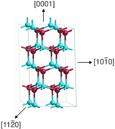 | ||
| Fig. 1 Wurtzite structure of bulk ZnO. Here and in the remainder of the figures, Zn atoms are depicted in light blue, O in red. The (0001), (100) and (110) directions are also shown. | ||
Section 2 presents further experimental data that explores and illustrates aspects of c-axis aligned ZnO film growth by PLD methods. Clarifying possible stabilisation mechanisms for the (0001) and (000) surfaces of ZnO remains an important issue. Sections 3 and 4 focus on a different but related question: Why does layer-by-layer growth of ZnO so readily yield the (0001) and (000) surfaces, rather than non-polar surfaces such as (100) and (110)? We investigate this problem by examining computed structures of thin films of ZnO, as a function of film thickness.
2. Experimental studies
ZnO thin films were grown by pulsed ArF laser ablation (Lambda-Physik COMPex 201, 193 nm, 10 Hz rep. rate) of a 99.999% pure ZnO hot pressed disk target (Cerac), which was rotated in order to prevent repeated ablation of the same area. Typical pulse energies used were ∼150 mJ which, when focused onto the target, produced an incident fluence of ∼10 J cm−2. The growth chamber was evacuated using a turbomolecular pump and then back filled with a steady flow of O2 so as to maintain a constant pressure, p(O2) = 10 mTorr. The substrates (single crystal Si throughout this study) were positioned 6 cm distant from the target and could be heated to ∼1000 K by illuminating the rear surface with the output from a continuous working (cw) CO2 laser (Synrad, model J48-2W-3180). All deposition runs in this work involved 27000 laser shots unless specified otherwise. Scanning electron microscopy (SEM, JEOL 6300LV) was used to provide visual images of the film morphology, and its variation with substrate temperature in the range 298 K < Tsub < 1023 K. The crystallinity and texture of the as-grown films were assessed by X-ray diffraction (XRD), using a Bruker AXS D8 Advance powder X-ray diffractometer.SEM analysis revealed that all films grown at Tsub < 723 K displayed a granular, polycrystalline morphology, and an increasing tendency for nanorod formation at higher Tsub.17 We return to explore this latter aspect further later in this Section. XRD spectra of all deposited films were dominated by the (0002) and (0004) basal plane reflections of wurtzite ZnO, thereby reinforcing previous reports that ZnO films produced by PLD methods grow with the (0001) direction parallel to the substrate normal.18–21Fig. 2 shows a number of 2θ scans, recorded in the vicinity of the (0002) reflection, and plotted on a semi-logarithmic scale. The peak is seen to gain in intensity, and to shift to somewhat higher angle, as Tsub is increased to ∼573 K, but to be relatively insensitive to further increases in substrate temperature. Given the wavelength (λ = 1.54056 Å) of the Cu Kα X-ray source used, the observed 2θ peak values (and their shift) imply a decrease in c-lattice parameter from 5.31 Å to 5.18 Å as Tsub increases from 298 K to 573 K (cf. a value of 5.213 Å for strain-free wurtzite ZnO). Adopting the biaxial strain model, such shifts would imply a change in strain in the deposited films, along the c-axis, from +2% to −0.5% over this range of Tsub.
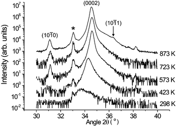 | ||
| Fig. 2 A selection of XRD 2θ plots of ZnO films grown by PLD in a low background pressure of O2, on Si substrates, as a function of Tsub. The displayed spectra, which are plotted on a logarithmic intensity scale, concentrate on the vicinity of the (0002) reflection. The peak at 2θ ∼ 33°, marked with an asterisk, is associated with the Si substrate. | ||
ω-rocking curves of the (0002) peaks were measured also, in order to characterize the extent of c-axis orientation and its variation with Tsub. As Figure 3 shows, the full width half maximum (FWHM) value of the rocking curve of the (0002) peak falls rapidly, from ∼11° in the case of the rather amorphous films grown at 298 K, to ∼2° for films grown at Tsub ≥ 573 K. These data, and the 2θ measurements, both indicate that deposition at elevated Tsub is very beneficial from the viewpoints of both crystal quality and the degree of orientational texturing, but that neither property is improved further by the use of Tsub values > 573 K. In this regard, the present findings involving Si substrates show many parallels with results reported previously for growth of polycrystalline ZnO films, by PLD, on sapphire substrates – though, in the case of sapphire, the coincidentally small lattice mismatch with ZnO allows a much greater degree of heteroepitaxy.9
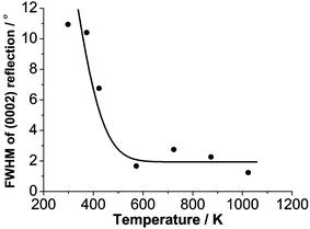 | ||
| Fig. 3 Plot illustrating the Tsub dependence of the FWHM of the (0002) rocking curve of ZnO films grown by PLD on Si. | ||
Given the foregoing observations, it was of interest to investigate the use of well-aligned ZnO thin films (i.e. films grown at Tsub = 573 K) as templates for further deposition. Fig. 4 shows 2θ scans in the region of the (0002) reflection, and the associated (0002) rocking curves, for four different ZnO films. All were grown, as before, on Si substrates, by PLD in p(O2) ∼10 mTorr, using 27 000 laser shots. Spectra (a) and (d) are of films deposited at Tsub = 373 and 573 K, respectively; the respective FWHM values of the associated rocking curves are 10.4° and 1.7°; these points were amongst the data presented Fig. 3. Spectra (b) and (c) are of films grown at Tsub = 573 K for, respectively, 1 and 2 min, after which time Tsub was reduced to 373 K and deposition continued to a total of 45 min. The FWHM values of the measured (0002) rocking curves are 3.7° and 3.1°, i.e. only about one third of the widths measured for material grown at Tsub = 373 K without pre-deposition at higher Tsub. Clearly an ultra-thin film of well-aligned material deposited in the first 1–2 min can indeed act as an aligning template for subsequent growth at much lower Tsub.
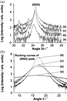 | ||
| Fig. 4 XRD 2θ scans of ZnO films in the region of the (0002) reflection, and the associated (0002) rocking curves, for four ZnO films. All were grown on Si substrates, by PLD, in p(O2) ∼10 mTorr, using 27000 laser shots and substrate temperatures as follows: (a) Tsub = 373 K, (b) Tsub = 573 K for 1 min, then Tsub = 373 K for 44 min, (c) Tsub = 573 K for 2 min, thereafter Tsub = 373 K for 43 min., and (d) Tsub = 573 K throughout. Again, the peak at 2θ ∼ 33° is due to the Si substrate. | ||
Fig. 5 provides another illustration of the effect of such ultra-thin template layers. Elsewhere we have shown that deposition at Tsub = 873 K can result in well-aligned arrays of needle-like nanorods of ZnO.17 As Fig. 5 shows, however, films deposited at a (constant) higher Tsub value (1023 K, images (a) and (c)) have a very different morphology, dominated by irregularly shaped crystallites with a low density of vestigial nanorods. These images should be contrasted with (b) and (d), which are of films produced by initial deposition at Tsub = 573 K for just 1 min, followed by a further 44 min deposition at Tsub = 1023 K. Once again, the ultra-thin film of well-aligned material deposited in the first minute dictates the morphology of material grown subsequently at a very different Tsub and, once again, the growth is very strongly c-axis aligned.
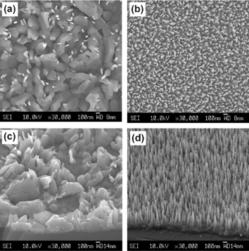 | ||
| Fig. 5 SEM images of ZnO films grown on Si substrates, by PLD, in p(O2) ∼10 mTorr, using 27000 laser shots and substrate temperatures as follows: (a) and (c): Tsub = 1023 K; (b) and (d): Tsub = 573 K for 1 min, followed by Tsub = 1023 K for a further 44 min. Images (a) and (b) show plan views, while (c) and (d) were recorded at a tilt angle of ∼40° to the horizontal. | ||
3. Theoretical methods
All calculations in this work were carried out using periodic plane-wave density functional theory (DFT) calculations in the generalized gradient approximation (GGA) as implemented in the CASTEP code22 with the Perdew–Wang exchange correlation functional23 We used the ultra-soft Vanderbilt pseudopotentials24 and an energy cutoff for the plane waves of 380 eV. The reciprocal space integration utilized the Monkhorst–Pack sampling scheme25 and we have checked the convergence of the energy with the number of k-points.ZnO adopts the wurtzite structure (Fig. 1) which does not possess a centre of inversion. The calculated bulk a- and c-lattice parameters and u are 3.270 Å, 5.218 Å, and 0.3822, which compare with experimental values of 3.253 Å, 5.213 Å, and 0.3820 respectively. To generate the thin films, we used the “supercell” approach: a suitably orientated supercell is periodically repeated in three dimensions so that an infinite set of slabs is produced, with each slab separated from its neighbours by a vacuum gap of ≈10 Å to ensure negligible interaction. Films terminating with the three most important low-index growth surfaces observed experimentally, the non-polar (100) and (110) and the polar (0001)/(000), were examined for film thicknesses ranging from 4 to 24 layers. Optimised structures for each film were obtained, relaxing all structural degrees of freedom, including the surface lattice vectors.
4. Results
We consider first the structure of each surface in turn (subsections a and b), and then examine surface energies (c) as a function of film thickness, before turning finally to film growth (d).a Non-polar (10![[1 with combining macron]](https://www.rsc.org/images/entities/h3_char_0031_0304.gif) 0) and (11
0) and (11![[2 with combining macron]](https://www.rsc.org/images/entities/h3_char_0032_0304.gif) 0) film geometries
0) film geometries
Details of the (100) surface are given in Fig. 6. Fig. 6a shows a side view of the slab, illustrating the stacking sequence perpendicular to the surface. Fig. 6b defines the surface unit cell employed, which contains two formula units and Fig. 6c depicts a further side view showing the set of labels employed in the discussion of the geometry of the slab. The surface consists of equal numbers of zinc and oxygen ions (Tasker Type I) and a useful description is that it consists of rows of Zn–O dimers. Initially a and b were set to 3.28 Å and 5.24 Å respectively. For all thicknesses significant changes in interlayer spacings relative to the bulk (>1%) were only seen between the first three surface layers (Table 1). In agreement with experiment26 and in line with other theoretical studies, both classical (potential-based)27 and ab initio,28,29 the Zn ions in the outermost layer contract inward while the Zn ions in the second layer move toward the surface, reducing the Zn–O bond length between the top two layers by ≈3%
(distance A in Fig. 6c). The O atoms remain close to their bulk positions. The relaxation shortens the bond in the Zn–O dimers in the surface layer by ≈7%
(distance B) and causes the dimer to tilt from its alignment perpendicular to the (100) direction. The O–Zn–O bond angle (angle θ) involving the top two layers changes from 108° in the bulk to 117°. This tilting is absent from the third and subsequent layers (for films with more than four layers) but the Zn–O bond length between the second and third layers is ≈3% larger (distance C) than the corresponding bulk value. As Table 1 shows, there is little change in the magnitude of the relaxations with slab thickness. Quantitatively our contraction in the Zn–O surface bond length is somewhat larger (≈0.05 Å) than that in the B3LYP studies of Wander and Harrison28 but very similar to that noted previously at the Hartree–Fock level.30 Our tilt angle θ is almost identical to the LDA (local density approximation) value of Meyer and Marx.29 All ab initio theoretical studies we have been able to find give a tilt angle smaller than that observed experimentally.31
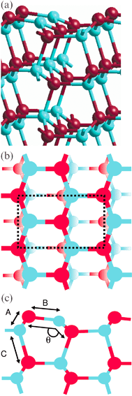 | ||
| Fig. 6 The relaxed (100) surface for a slab containing 16 layers. (a) side view showing the stacking sequence perpendicular to the surface. Only the top six layers are shown. (b) top view showing the surface unit cell (dotted lines)
(c) side view showing the dimers at the surface and the labels used to discuss the geometry at the surface. | ||
0) films of varying thickness. Labels refer to separations marked in Fig. 6c. Values are given separately for the surface layers and the mean value for the slab interior (excluding the surface layers). The ‘bilayer separation (A)’ is the separation between layers 1–2, 3–4, 5–6 etc. The Zn–O dimer bond length (B) is the Zn–O bond length within the same layer. Layer separation (C) refers to the separation between layers 2–3, 4–5, 6–7 etc.
| Number of layers | Bilayer separation (A)/Å | Zn–O dimer bond length (B)/Å | Layer separation (C)/Å | |||
|---|---|---|---|---|---|---|
| First–second layer | Slab Interior | Surface layer | Slab Interior | Second–third layer | Slab Interior | |
| 8 | 1.929 | 1.983 | 1.854 | 1.998 | 2.067 | 2.015 |
| 10 | 1.932 | 1.981 | 1.854 | 1.997 | 2.060 | 2.010 |
| 12 | 1.926 | 1.985 | 1.852 | 1.997 | 2.057 | 2.003 |
| 14 | 1.925 | 1.985 | 1.853 | 1.998 | 2.049 | 1.992 |
| 16 | 1.924 | 1.984 | 1.853 | 1.997 | 2.056 | 1.996 |
| 18 | 1.925 | 1.984 | 1.849 | 1.988 | 2.060 | 1.991 |
| 20 | 1.926 | 1.986 | 1.857 | 1.999 | 2.064 | 1.994 |
| 22 | 1.924 | 1.984 | 1.859 | 1.998 | 2.058 | 1.991 |
| 24 | 1.931 | 1.983 | 1.858 | 1.999 | 2.054 | 1.991 |
The (110) surface and the corresponding surface unit cell are shown in Fig. 7a–b. This surface is similar to (100)
(Tasker Type I), but the surface unit cell is larger containing four formula units. Again a useful description is in terms of rows of Zn–O dimers, which now form zig-zag lines across the surface. Initially a and b were set to 5.66 Å and 5.23 Å respectively. As for (100), the Zn ions in the outermost layer contract inward toward the bulk while the remainder of the ions remain essentially stationary. This reduces the Zn–O bond length between the two outermost layers by ≈2%
(distance D in Fig. 7c) and shortens the Zn–O bond in the surface dimers by ≈6%
(distance E). Again the surface dimers tilt from their position parallel to the surface causing the O–Zn–O bond angle (φ) involving the top two layers to increase to 116° from the bulk value of 108°. The relaxations of the (110) slabs are similar but not as marked as those for the (100) slabs; we do not see the same shift of the top two layers away from the slab (i.e. an increase in layer 2 – layer 3 separation) or any appreciable atomic relaxation in the second layer. The results are in good quantitative agreement with those calculated by Meyer and Marx.29 However, there is a marked discrepancy with the study of Wander and Harrison32 who have reported little relaxation of the slab and a cleavage energy approximately double that found in the current work (see section c). Meyer and Marx have attributed this discrepancy to symmetry restrictions placed on the ion positions in ref. 32, which prevent intralayer motion of the Zn ions and the dimers from adopting the tilt geometry.
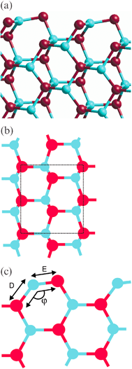 | ||
| Fig. 7 The relaxed (110) surface for a slab containing 14 layers. (a) side view showing the stacking sequence perpendicular to the surface. Only the top six layers are shown. (b) top view showing the surface unit cell (dotted lines)
(c) side view showing the dimers at the surface and the labels used to discuss the geometry at the surface. | ||
All solutions were insulating for films terminating with the (100) and (110) surfaces.
b Polar film geometries
Cleaving ZnO perpendicular to the c-axis creates Zn-terminated (0001) and O-terminated (000) surfaces (Tasker Type III), as shown in Fig. 8a. The surface unit cell now comprises just one ion (Zn or O respectively)
(Fig. 8b). In a formal ionic model the surface energy, defined as the difference between the energy of the slab and the energy of the same number of formula units in the bulk, diverges with slab thickness and such polar surfaces are unstable, in the absence of charge rearrangement. In the absence of a change in surface layer composition this may be achieved by a charge transfer from the valence band at the O-terminated surface to the conduction band at the Zn-terminated surface.
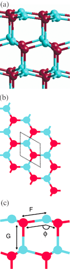 | ||
| Fig. 8 The (0001) and (000) surfaces. (a) Stacking sequence in unrelaxed slab perpendicular to the surfaces (b) top view showing the surface unit cell (dotted lines)
(c) side view of the relaxed (0001) surface of the slab containing 20 layers. Only the top four layers are shown. Figure shows the labels used to discuss the geometry of the surface. | ||
For a film thickness of >18 layers the electronic structure of the slab is consistent with such a charge transfer. The resulting electronic structure is similar to the “surface metallization” solution, shown schematically in Fig. 9. Wander et al.,14 in their B3LYP study, and Carlsson's15 DFT calculations have also found the same solution. We stress again we have not considered non-stoichiometric surfaces and any possible stabilization mechanisms resulting therefrom.
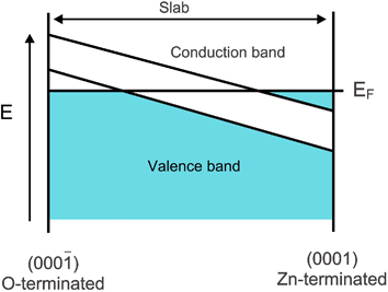 | ||
| Fig. 9 Band structure diagram (schematic) of the surface metallization solution for the slab terminating with the (0001) and (000) surfaces. | ||
For films with >18 layers the relaxed structure of the films is in general agreement with that proposed in previous theoretical studies.14,15,29Fig. 8c is a side view of the top 4 layers (Zn-termination) of a relaxed 20-layer slab, clearly showing a substantial change in bond angles. We label the Zn terminated surface layer as 1. Alternate layers (e.g., pairs 1 and 2, or 3 and 4) are close together, effectively forming a series of Zn–O bilayers. Within a bilayer Zn–O bond lengths (e.g., distance F in Fig. 8c) contract from their bulk separation causing the layers that make up each bilayer to move closer together. In marked contrast, Zn–O bonds between bilayers (distance G between layers 2 and 3) expand. These effects increase closer to the Zn and O-terminated surfaces, as shown by the values listed in Table 2 and the variation in bond length with depth plotted in Fig. 10. The mean contraction of the Zn–O bonds within the bilayers is ≈1%, and the expansion between the layers a striking ≈4%. These relaxations also cause a shift in the O–Zn–O bond angles within the film away from the bulk values of 108.2° (within a bilayer) and 110.7° (between bilayers). Once more, this is depth dependent, decreasing away from the surface. The mean O–Zn–O bond angle within the bilayers increases to ≈113° while that between the bilayers decreases to ≈105°. Overall, each Zn within the film shifts away from regular tetrahedral coordination towards an environment in which each Zn has three nearest O neighbours within the bilayer, and a further oxygen neighbour at a greater distance in the next bilayer. The relaxation is more marked at the O-terminated than the Zn-terminated surface; the Zn–O bond at the former is 0.5% shorter, and the separation between the first two bilayers 0.8% greater.
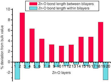 | ||
| Fig. 10 Variation of Zn–O bond length with depth in a film of 20 layers terminating with the (0001) and (000) surfaces. Layer 1 is Zn-terminated, layer 20 O-terminated. For a discussion of the bilayers, see text. | ||
| Number of layers | Mean Zn–O bond length within bilayers (F)/Å | Mean Zn–O bond length between bilayers (G)/Å | ||
|---|---|---|---|---|
| Surface | Slab interior | Surface | Slab interior | |
| 18 | 1.925 | 1.968 | 2.143 | 2.065 |
| 20 | 1.923 | 1.971 | 2.161 | 2.077 |
| 22 | 1.925 | 1.973 | 2.154 | 2.054 |
| 24 | 1.925 | 1.975 | 2.139 | 2.047 |
Thinner films with <18-layers behave very differently. These are unstable and flatten on optimisation, yielding ‘graphitic-like’ ZnO layers (Fig. 11), in which each atom is three-fold coordinate. These are stacked AB on top of each other such that a Zn is above an O, and vice versa. A six-layer unrelaxed film (comprising three bilayers) thus yields after optimisation a three-layer film (although we shall continue to refer to it as a six-layer film in our discussion). Intralayer bond lengths (1.93 Å) differ substantially from those in the bulk (≈3% shorter) and the O–Zn–O bond angles have changed from 108.2° to 120°. The interlayer separation is ≈2.4 Å and does not vary significantly with slab thickness. This solution is insulating unlike the surface metallization solution for films with >18 layers. In passing we note that at the non-polar (100) and (110) surfaces the tilt in the surface Zn–O dimers and the relaxation in the surface bilayers at the polar (0001) surfaces of thicker films metal shift the surface geometry closer to that of the graphitic system. Surface flattening has also been observed in first principles DFT calculations of GaN on SiC where the ultra-thin film of GaN forms flat layers rather than adopting a bulk wurtzite structure.33
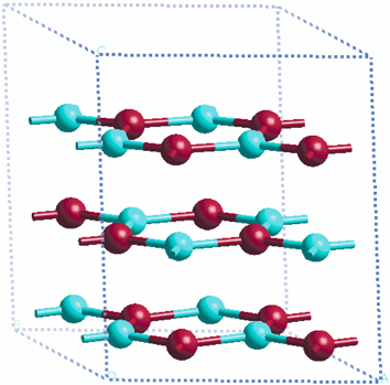 | ||
| Fig. 11 The graphitic ZnO layers. | ||
In the wurtzite phase of ZnO the Zn3O3 hexagonal rings are arranged in the ‘boat’ and ‘chair’ conformations. These rings are flat in the graphitic sheets. In the course of this work we have also carried out a small number of geometry optimisations on isolated Zn3O3 molecular clusters of the boat, chair and flat form at the B3LYP34–37 level of theory using the Jaguar program38 with the LACVP basis set.39 Upon optimisation all the rings optimise to a flat geometry with O–Zn–O bond angles of ≈140° and bond Zn–O bond lengths of 1.86 Å. Calculations on larger clusters of three interlinked hexagonal rings (Zn7O6) show the same flattening but now the O–Zn–O bond angles where the rings link are ≈120° while those on the edge of the cluster are ≈140°. The Zn–O bond lengths also vary with values of 1.91 Å at the edge and 1.99 Å in the centre of the cluster. These results all serve to illustrate the tendency of ZnO units to adopt a flat structure under certain conditions.
c Surface and cleavage energies
Cleavage energies are shown as a function of film thickness in Fig. 12. Note that no unique surface energy can be determined for the (0001)-Zn and the (000)-O surfaces since both surfaces are present, and the value plotted is the cleavage energy; for the non-polar surfaces the cleavage energy is simply twice the surface energy. For the graphitic surface the number of layers is that before optimisation, i.e., the number of layers in the final optimised film is half the starting number. Values plotted for the (0001) surface for films of ≤16 layers are from restricted calculations since, as we have seen, they are unstable and rapidly converge on optimisation to the graphitic, insulating solution.
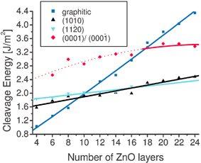 | ||
| Fig. 12 Cleavage energies (in J m−2) as a function of film thickness. For the graphitic surface the number of layers plotted is that before optimization, i.e., the number of layers in the final optimized film is half the initial number. Values plotted for the (0001) film for <18 layers are unoptimised values before relaxation since they are unstable with respect to the graphitic, insulating solution, i.e., they do not correspond to local minima on the potential energy hypersurface. | ||
As expected the surface energy of the polar surface is greater than the non-polar (100) and (110) surfaces for all film thicknesses. However, the graphitic-like surface is lowest in energy for <10 layers, and thus more stable than the two non-polar surfaces studied for these thin films. For slab sizes of 10–18 layers, this surface is higher in energy than the two non-polar solutions but lower in energy than the metallic solution. For films with >18 layers the metallic solution is lower than the graphitic for the (0001) surfaces.
d Thin film growth
On purely energetic considerations the results of the previous section suggest that when the number of layers is >10 the morphology should be dominated by the (100) and (110) surfaces. So why does the polar (0001) surface appear? The results of the previous section hint at a possible growth mechanism in which the first few layers deposited adopt the graphitic-like structure. What are the possible implications of the formation of this structure? Structurally the graphitic film is very different from films which terminate with the (100) or (110) surfaces. In the graphitic like structure the Zn and O ions in alternate layers lie directly above each other. In contrast alternate ZnO layers in the (100) slab are shifted relative to each other (Fig. 6b) while in the (110) slab the Zn ions (and therefore the O ions) lie directly above and below each other in alternating bilayers (Fig. 7a, b and c). Additionally the Zn3O3 rings that make up the film adopt different conformations in each case: a flat conformation is adopted in the graphitic system, and boat and chair conformations in the (100) and (110) films.
We have estimated the magnitude of the energy barrier for the transition from the graphitic-like to the (100) film. For the purposes of defining a possible mechanism (i.e., a specific atomic pathway) and its practical calculation, the potential energy hypersurface must clearly be reduced to no more than a few dimensions. This is achieved by assuming that some degree of periodicity is retained in the course of the transition, so that the mechanism of the transition can be defined in terms of the size and symmetry of the repeat unit connecting the two phases.40 Retention of periodicity implies that the phase transition is a cooperative process involving a concerted movement of atoms with no account of possible rôles played by defects.
We have assumed a surface unit cell containing two formula units, which is the minimum necessary to construct the primitive cell of the (100) surface. Most mechanisms require extensive atomic rearrangements involving extensive bond-breaking with large activation energies. Ignoring relaxation, we can write one possible mechanism in terms of the unit cell variables and atom positions (Scheme 1).
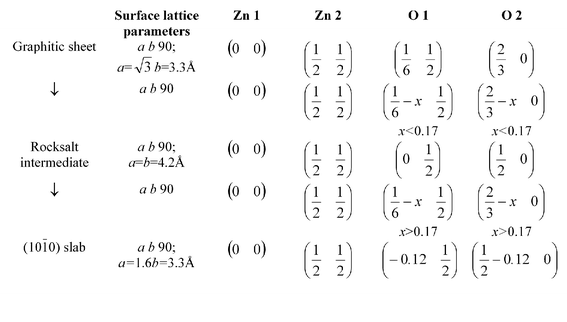 | ||
| Scheme 1 | ||
In the final stage, the transition from the rock-salt to the (100) film, the second layer in the rocksalt structure, which is the same as the top layer but displaced by b/2, undergoes the same atomic motions with the oxygens moving in the same direction, In addition alternate rows of atoms parallel to the a-axis are displaced up and down perpendicular to the surface as shown in Fig. 13a and b. The choice of the rocksalt intermediate is reasonable given that bulk ZnO itself undergoes a transition to the NaCl-type structure at pressures as low as 9 GPa.41 Our mechanism displays features of the wurzite to rocksalt GaN transition proposed by Limpijumnong et al.42 who have identified an intermediate structure (termed h-MgO) similar to our graphitic solution where the bilayers have flattened before adopting the rocksalt geometry.
 | ||
| Fig. 13 Possible mechanism of the transformation between the graphitic and (100) morphologies via a rocksalt (001) film intermediate (a) side view (b) top view. | ||
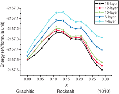
Energies were calculated at thirteen points along the pathway, assuming a uniform variation in the lattice parameters a and b along the path. At each point an optimisation is performed keeping these cell lattice parameters fixed, but imposing no constraints on any of the atomic positions within the slab. The resulting energy pathways for 4, 6, 10, 12 and 16-layer films are displayed in Fig. 14. We label the reaction coordinate using the corresponding value of the displacement coordinate x. The local minima approximately halfway along each path correspond to the rocksalt intermediate. The barrier height decreases with slab thickness, varying from ≈0.5 eV (formula unit)−1 for the four-layer film to ≈0.3 eV (formula unit)−1 for the thicker ten-layer slab and there is relatively little change for thicker slabs thereafter.
 | ||
| Fig. 14 Energy pathway for the transformation shown in Fig. 13, as a function of reaction coordinate x, as defined in the text. All energies are per formula unit. | ||
We have investigated one further route across the potential hypersurface which does not involve the rocksalt intermediate. The unit cell is the same size as above, and the mechanism is such that every second layer undergoes a set of displacements (Fig. 15, Scheme 2)
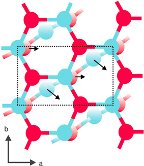 | ||
| Fig. 15 Alternative mechanism for the transformation between the graphitic and (100) morphologies | ||
 | ||
| Scheme 2 | ||
One analysis of the zinc-blende to rocksalt transition43 has suggested the Zn moves from tetrahedral to octahedral geometry by crossing through a triangular plane of O ions. Fig. 15 shows a similar process for the Zn ions in our second mechanism where two O ions lie in the same layer and the third O is in the layer above. This pathway is considerably higher in energy with a barrier height that is typically twice that of the comparable film thicknesses in Fig. 14.
We stress that it is unlikely we have identified the minimum energy barrier as the extensive search of the potential energy hypersurface required is beyond current resources for a system of this complexity. Nevertheless our results suggest that conversion between the graphitic to the (100) film is an activated process with a substantial barrier even when the transition is thermodynamically favourable. The structural dissimilarity between the graphitic and (110) geometries and the similarity between the (110) and (100) geometry is such that the barrier for transition from the graphitic to the (110) film would not be expected to differ substantitially from that to (100).
In contrast there is no energy barrier in analogous calculations for the conversion from the graphitic to the (0001) morphology for comparable number of layers. Beyond 20 layers this transition becomes thermodynamically favourable, and increasingly so for thicker films. The mechanism is much simpler, involving only a buckling of the Zn3O3 rings. No relative translation of alternate layers is required. Overall, our results suggest that when the number of graphitic layers increases beyond six and the graphitic structure becomes thermodynamically unstable, the existence of an energy barrier prevents conversion to the (100) and (110) films. Instead as the depth increases for thicker films there is a barrierless transition to the (0001) morphology.
5. Conclusions
In this paper we have presented experimental evidence related to the domination of the morphology of ZnO thin films by the polar (0001) surfaces. We have also examined computationally the structure of thin films of ZnO terminating with the (0001), (000), (100) and (110) surfaces, and noted the stability, for very thin films, of a new structure –
graphitic layers made up of hexagonal Zn3O3 rings. We have discussed the implications of the formation of such layers for the thin film growth and have suggested a possible growth mechanism involving these layers which leads to the formation of (0001) films in preference to termination by a non-polar surface. Since submitting this paper we have become aware of a very recent experimental study by Hur et al.44 of the structural evolution of ZnO thin films by in situ synchrotron x-ray scattering, which is consistent with this model.
Acknowledgements
This work is supported by a number of ESPRC grants and HEFCE JREI awards, including the portfolio partnership LASER. The Bristol team is grateful to the University of Bristol and the Overseas Research Scholarship (ORS) scheme for the award of a postgraduate scholarship (to Ye Sun), and to J. Charmant, S. A. Davis, G. M. Fuge, S. J. Henley (now at the University of Surrey) and K. N. Rosser for their many and varied contributions to the experimental work described herein.References
- D. C. Look, Mater. Sci. Eng. B, 2001, 80, 383 CrossRef.
- M. H. Huang, S. Mao, H. Feick, H. Q. Yan, Y. Y. Wu, H. Kind, E. Weber, R. Russo and P. D. Yang, Science, 2001, 292, 1897 CrossRef CAS.
- X. Feng, L. Feng, M. Jin, J. Zhei, L. Jiang and D. Zhu, J. Am. Chem. Soc., 2004, 126, 62 CrossRef CAS.
- Z. L. Wang, Mater. Today, 2004,(June), 26 Search PubMed , and references therein.
- Z. R. Tian, J. A. Voigt, J. Liu, B. McKenzie, M. J. McDermott, M. A. Rodriguez, H. Konishi and H. Xu, Nat. Mater., 2003, 2, 821 CrossRef CAS.
- K. Govender, D. S. Boyle, P. B. Kenway and P. O'Brien, J. Mater. Chem., 2004, 14, 2575 RSC.
- S. J. Henley, M. N. R. Ashfold and D. Cherns, Surf. Coat. Tech., 2004, 177, 271 CrossRef.
- S. J. Henley, M. N. R. Ashfold and D. Cherns, Thin Solid Films, 2002, 422, 69 CrossRef CAS.
- X. W. Sun and H. S. Kwok, J. Appl. Phys., 1999, 86, 408 CrossRef CAS.
- L. Niinisto, J. Paivasaari, J. Niinisto, M. Putkonen and M. Nieminen, Phys. Status Solidi A, 2004, 201, 1443 CrossRef , and references therein.
- P. W. Tasker, J. Phys. C, 1979, 12, 4977 CrossRef CAS.
- C. Noguera, J. Phys.: Condens. Matter, 2000, 12, R367 CrossRef CAS.
- O. Dulab, L. A. Boatner and U. Diebold, Surf. Sci., 2002, 519, 201 CrossRef.
- A. Wander, P. Schedin, P. Steadman, A. Norris, R. Mcgrath, T. S. Turner, G. Thornton and N. M. Harrison, Phys. Rev. Lett., 2001, 86, 3811 CrossRef CAS.
- J. M. Carlsson, Comp. Mat. Sci., 2001, 22, 24 Search PubMed.
- A. Wander and N. M. Harrison, J. Chem. Phys., 2001, 115, 2312 CrossRef CAS.
- Y. Sun, G. M. Fuge and M. N. R. Ashfold, Chem. Phys. Lett., 2004, 396, 21 CrossRef.
- V. Craciun, J. Elders, J. G. E. Gardiniers, J. Gretovsky and I. W. Boyd, Thin Solid Films, 1995, 259, 1 CrossRef CAS.
- R. D. Vispute, V. Talyansky, Z. Trajanovic, S. Choopun, M. Downes, R. P. Sharma, T. Venkatesan, M. C. Woods, R. T. Lareau, K. A. Jones and A. A. Iliadis, Appl. Phys. Lett., 1997, 70, 2735 CrossRef.
- M. Hiramatsu, K. Imaeda, N. Horio and M. Nawata, J. Vac. Sci. Technol. A, 1998, 16, 669 CrossRef CAS.
- J. H. Choi, H. Tabata and T. Kawai, J. Cryst. Growth, 2001, 226, 493 CrossRef CAS.
- CASTEP 4.2 academic version, licensed under the UKCP-MSI Agreement, 1999 Search PubMed; M. C. Payne M. P. Teter D. C. Allan T. A. Arias J. D. Joannopoulos Rev. Mod. Phys., 1992, 64, 1045 Search PubMed.
- J. P. Perdew and Y. Wang, Phys. Rev. B, 1992, 45, 13244 CrossRef.
- D. Vanderbilt, Phys. Rev. B, 1990, 41, 7892 CrossRef.
- H. J. Monkhorst and J. D. Pack, Phys. Rev. B, 1976, 13, 5188 CrossRef.
- N. Jedrecy, A. Gallini, M. Sauvage-Simkin and R. Pinchaux, Surf. Sci., 2000, 460, 136 CrossRef CAS.
- L. Whitmore, A. A. Sokol and C. R. A. Catlow, Surf. Sci., 2002, 498, 135 CrossRef CAS.
- A. Wander and N. M. Harrison, Surf. Sci., 2000, 457, L342 CrossRef CAS.
- B. Meyer and D. Marx, Phys. Rev. B, 2003, 67, 35403 Search PubMed.
- J. E. Jaffe, N. M. Harrison and A. C. Hess, Phys. Rev. B, 1994, 49, 11153 CrossRef CAS.
- C. B. Duke, D. L. Lessor, T. N. Horsky, G. Brandes, K. F. Canter, P. H. Lippel, A. P. Mills, A. Paton and Y. R. Wang, J. Vac. Sci. Technol. A, 1989, 7, 2030 CrossRef CAS.
- A. Wander and N. M. Harrison, Surf. Sci., 2000, 468, L851 CrossRef CAS.
- R. B. Capaz, H. Lim and J. D. Joannopoulos, Phys. Rev. B, 1995, 51, 17755 CrossRef CAS.
- A. D. Becke, J.Chem.Phys., 1993, 98, 5648 CrossRef CAS.
- C. Lee, W. Yang and R. G. Parr, Phys. Rev. B, 1988, 37, 785 CrossRef CAS.
- S. H. Vosko, L. Wilk and M. Nusair, Can. J. Phys., 1980, 58, 1200 CrossRef CAS.
- P. J. Stephens, F. J. Devlin, C. F. Chabalowski and M. J. Frisch, J. Phys. Chem., 1994, 98, 11623 CrossRef CAS.
- Jaguar 5.5, Schrödinger, Portland, OR, 1991–2003 Search PubMed.
- P. J. Hay and W. R. Wadt, J. Chem. Phys., 1985, 82, 299 CrossRef CAS.
- E.g., C. E. Sims, G. D. Barrera, N. L. Allan and W. C. Mackrodt, Phys. Rev. B, 1998, 57, 11164 Search PubMed.
- F. Decremps, J. Pellicer-Porres, A. M. Saitta, J.-C. Chervin and A. Polian, Phys. Rev. B, 2001, 65, 92101 Search PubMed.
- S. Limpijumnong and R. L. Lambrecht, Phys. Rev. Lett., 2001, 86, 91 CrossRef CAS.
- M. A. Blanco, J. M. Recio, A. Costales and R. Pandey, Phys. Rev. B, 2000, 62, R10599 Search PubMed.
- T.-B. Hug, Y.-H. Hwang, H.-K. Kim and H.-L. Park, J. Appl. Phys., 2004, 96, 1740 CrossRef.
| This journal is © The Royal Society of Chemistry 2005 |