Control of semiconducting oxide gas-sensor microstructure by application of an electric field during aerosol-assisted chemical vapour deposition
Graham
Shaw
a,
Ivan P.
Parkin
*a,
Keith F. E.
Pratt
a and
David E.
Williams
b
aChristopher Ingold Laboratories, University College London, UK WC1H 0AJ. E-mail: i.p.parkin@ucl.ac.uk
bUnipath Limited, Priory Business Park, Bedford, UK MK44 3UP
First published on 15th October 2004
Abstract
Tungsten oxide thin films were deposited on gas sensor substrates from the aerosol assisted chemical vapour deposition of [W(OPh)6] in toluene at 600 °C. It was found that application of an electric field during deposition encouraged thicker film growth. The morphology of the tungsten oxide film could be altered by using stronger electric fields and by use of both direct and alternating currents. In particular the use of alternating currents produced aligned fibrous growth between the electrode gaps of the sensor substrate. This morphology produced a tungsten oxide gas sensor that was particularly sensitive to low concentrations of nitrogen dioxide.
Introduction
Porous semiconducting metal oxide films have been widely studied as heterogeneous, solid state catalysts for the atmospheric combustion of a target gas.1 They have been incorporated into commercial devices by coating the gas sensitive oxide onto an interdigitated electrode array. The device works by measuring the changes in electrical resistance of the semiconducting oxide in the presence of trace gasses. Although unresolved questions exist concerning the details of the surface reactions and surface species, in practical devices it is crucial to control microstructure, since this directly affects gas sensitivity and discrimination by allowing surface states to dominate.1–3 Commercial demands for solid-state oxide gas sensors typically include high sensitivity and response to low gas concentrations. Microstructure modelling shows that the morphology of an ideal gas sensor should exhibit a high ratio of surface to bulk atoms, since the gas-sensing is largely a surface phenomenon.4–8 Consequently a range of ‘idealised’ microstructures exist that would be suitable for low gas concentrations, these include thin, highly dense films and extended fibres of the order of a hundred nanometres thick.9–11 A further requirement is to ensure good electrical contact with material localised between the electrodes. Control is therefore required over the amount of material, its localisation and orientation.We show here, for the first time, that one idealised microstucture can be achieved by the application of an applied electric field across the substrate during deposition. The use of ac rather than dc fields gives orientated fibres, and increasing the ac frequency confines growth to the electrode gap. To the best of our knowledge, this is the first time that WO3 gas sensors comprising controlled growth of extended nanofibres have been prepared in a commercially compatible, single-step process. More fundamentally the work shows that variable electric fields can control microstructure in an aerosol-assisted chemical vapour deposition (AACVD) process. The control of microstructure has enabled a gas sensor to be made that is significantly more sensitive to low concentrations of NO2 than conventional commercial sensors.
Experimental
Synthesis of [W(OPh)6]
[W(OPh)6] was prepared by the following procedure, using Schlenk techniques, under nitrogen. Phenol (14.1 g, 150 mmol) was added to a stirred solution of WCl6 (9.9 g, 25 mmol) in toluene (250 cm3) at reflux for 16 h. Solvent was removed in vacuo and the crude product heated at 80–90 °C for 3 h to remove unreacted phenol. From this point, materials were handled in air. The red solid was dissolved in ether (200 cm3) and washed with ca. 5% aqueous NaOH (3 × 100 cm3). The ether was removed in vacuo, with the resultant red solid subsequently dissolved in acetonitrile and filtered to remove undissolved residue. Removing the solvent in vacuo afforded a product that was pure by NMR spectroscopy (yield 8.75 g, 47%). 1H NMR (CDCl3): δ 6.86 (18 H, m, CH); δ 7.21 (12 H, m, CH). 13C NMR (CDCl3): δ 120.4 (CH); δ 123.4 (CH); δ 128.8 (CH); δ 161.8 (CO).Deposition of WO3−x
AACVD experiments were carried out in a horizontal-bed cold-wall reactor held at ambient temperature, with a blank sensor inserted into the rig at right angles to the direction of gas flow. Each sensor consisted of a 3 mm by 3 mm alumina substrate onto which was screen-printed gold electrodes of ca. 10 µm thickness which were screen-printed with an interdigitated pattern (finger and gap width of 100 µm and 60 ± 10 µm respectively). The reverse side of the sensors held a platinum heater track that formed one arm of a Wheatstone bridge, allowing the resistance, and so the heater temperature, to be both programmed and regulated.12 A dielectric was painted over the platinum heater in order to avoid forming an electrical connection of WO3−x between the deposited film and the heater track, thus effecting subsequent temperature regulation. An external power supply was used to generate a potential difference across the electrode gap during deposition, generating an electric field strength ≤1000 V cm−1 (current ∼ 5 mA).The apparatus used for AACVD was of in-house design, as described in the literature13 and shown in Scheme 1. [W(OPh)6] was dissolved in 50 cm3 of toluene to a concentration of 0.05 mmol, and an aerosol was generated at room temperature by use of a PIFCO air humidifier. Nitrogen was passed through the aerosol mist, thus forcing the aerosol droplets containing the precursor into the reactor chamber. All CVD experiments were performed with a nitrogen flow of 1 dm3 min−1. The carrier gas containing the aerosol mist was delivered to the heated substrate at ambient temperature. Deposition experiments were carried out at 600 °C (using the Pt heater to heat the sensor chip) until all of the precursor solution had been used, typically 90 min. On-chip annealing was performed at 600 °C for 2 h in synthetic air.
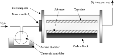 | ||
| Scheme 1 Diagrammatic plan of the apparatus used in the deposition. Note that the sensor substrate was placed between the top plate and bottom glass substrate, perpendicular to the flow of gas. | ||
General experimental
Glancing angle X-ray diffraction studies (1.5° coincident to plane) were carried out on films deposited on horizontal pieces of SiO2-coated float glass at 600 °C, using a Siemens D5000 diffractometer in reflection mode with monochromated Cu Kα1 radiation (λ = 1.5406 Å). X-Ray photoelectron spectroscopy was undertaken for both pre- and post-annealed films using a VG ESCALAB 220I XL instrument with focussed (300 µm spot) monochromatic Al Kα radiation at a pass energy of 20 eV. Scans were acquired with steps of 50 meV. A flood gun was used to control charging. Binding energies were referenced to an advantitious C 1s peak at 284.6 eV. Argon sputtering was used for approximately 1 min in a rastering mode in order to remove surface contamination. Energy dispersive analysis by X-rays was carried out on an Hitachi S570 with SEM images recorded at 10 KeV. The KEVEX system was used for the processing of both image and energy dispersions. Quantitative analyses were obtained at 20 KeV with reference to a cobalt source. Raman spectra were acquired on a Renishaw Raman System 1000 using a helium–neon laser (λ = 632.8 nm).Results and discussion
Synthesis
Aerosol-assisted chemical vapour deposition (AACVD) experiments were carried out with a horizontal-bed cold-wall reactor held at ambient temperature, with a blank, self-heated sensor12 inserted into the rig at right angles to the direction of gas flow. The temperature during deposition was 600 °C. An external power supply was used to generate a potential difference across the sensor electrode gap during deposition, generating an electric field strength ≤ 1000 V cm−1 (current ∼ 5 mA). The voltage variations applied were: A 1, 5, 10 and 20 V dc; B 1, 5 and 10 V ac (rms voltage at 50 Hz); and C 10, 50 and 1000 Hz at 5 V rms. Tungsten oxide was deposited over the sensor substrate by AACVD of [W(OPh)6] in toluene. On-chip annealing (600 °C in air) was performed to convert WO3−x to WO3 and remove carbon contamination from the film. Prolonged heat treatment (2 h) resulted in sintered fibres, thereby affording a stable morphology and so enabled a stable baseline resistance to be recorded.Synthesis and characterisation of fibrous films
The decomposition of [W(OPh)6] at 600 °C in a N2 gas stream under AACVD afforded a dark blue film of the characteristic colour of reduced tungsten trioxide (WO3−x). Upon annealing at 600 °C in air the film was observed to readily change colour to pale yellow within 15 min, characteristic of fully oxidised WO3. EDAX of both the pre- and post-heat-treated samples confirmed the presence of tungsten and oxygen in the expected elemental ratios, with carbon contamination of <2 at% prior to annealing. XPS was undertaken for both pre- and post-annealed films, with the expected chemical species observed for WO3−x (x = 0.1) and WO3. For the sintered films single environments were observed for both the O 1s (530.0 eV) and W6+ 4f doublet (4f7/2 35.6 eV; 4f5/2 37.8 eV), which are in excellent agreement with literature.14,15 The as-deposited films showed similar binding energies (O 1s 530.4 eV; W6+ 4f7/2 35.4 eV; W6+ 4f5/2 37.5 eV), with the addition of a shoulder to the 4f doublet at lower binding energies, suggesting the presence of W5+ or W4+ cations.14–16 These reduced species give strong evidence for the WO3−x stoichiometry. Raman spectroscopy of the films as deposited at 600 °C showed absorption peaks at 807, 715, 273 and 133 cm−1 characteristic of crystalline, monoclinic17,18 γ-WO3. In addition, an absorption peak at 208 cm−1 can be assigned to reduced tungsten cations, suggesting the film to be WO3−x. Sintering in O2 at 600 °C resulted in the loss of this characteristic absorption at 208 cm−1 and an increase in intensity of the remaining peaks.Observation of the effect of applied electric field upon fibre morphology
Deposition of WO3 on a sensor substrate from the AACVD of [W(OPh)6] in the absence of an electric field produced material that was localised at the electrode–alumina interface with virtually no growth across the electrode gap. However, if an electric field was applied across the sensor during deposition, it was observed that extended fibres dominated the morphology.SEM showed that all the depositions in an applied electric field gave fibrous growth of similar fibre thickness, 50–75 nm, yet the fibres differed in orientation and density over the sensor depending upon the electric field gradient, Fig. 1. At sufficiently high potential difference (20 V dc), multiple layers of extensive vertical growth were observed. For both ac and dc fields, an increase in applied voltage led to an increase in deposited material.
![Typical fibres afforded via AACVD by the decomposition of [W(OPh)6] in the electrode gap under an applied field. a, Fibres deposited in 1 V dc applied field (scale bar has a width of 1 µm). b, Fibres deposited in 1 V rms field at 50 Hz (scale bar has a width of 2 µm).](/image/article/2005/JM/b411680a/b411680a-f1.gif) | ||
| Fig. 1 Typical fibres afforded via AACVD by the decomposition of [W(OPh)6] in the electrode gap under an applied field. a, Fibres deposited in 1 V dc applied field (scale bar has a width of 1 µm). b, Fibres deposited in 1 V rms field at 50 Hz (scale bar has a width of 2 µm). | ||
For 1–5 V dc material was largely localised at the electrode–alumina interface as anisotropically orientated needle growth. In addition, a thin film was deposited across the electrode gap with randomly orientated fibrous growth emanating from the surface. No significant growth was observed on the electrode surface. A minimum bias voltage was thus deemed to be required in order for the electric field effects to override turbulent aerosol flow. This was achieved at 10 V dc with the observation of a new microstructure profile, Fig. 2. Growth was limited to the surface of the negative electrode as thicker, randomly orientated fibres. Electrical contact between the electrodes was achieved through deposition of a dense, solid film.
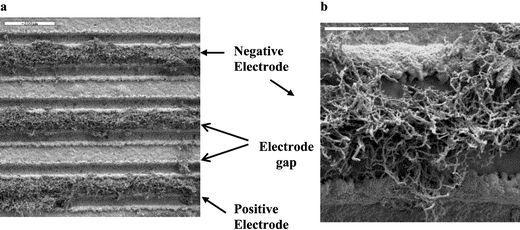 | ||
| Fig. 2 Deposition across an electrode array in an applied field of 10 V dc a, Fibrous growth is localised on the surface of the negative electrode only (scale bar has a width of 200 µm). b, The material as deposited on the negative electrode comprise thick, randomly orientated fibres (scale bar has a width of 50 µm). | ||
In comparison to a constant electric field, the use of 50 Hz ac (at 1 V, 5 V and 10 V rms) afforded extensive, randomly orientated fibrous growth away from the surface of both electrodes, with highly orientated fibres deposited between the electrodes (1 V rms; Fig. 3). Growth away from the sensor surface was so extensive for a 10 V ac field so as to obscure the electrode pattern, Fig. 4. The apparent increase in the amount of material deposited for a given voltage under ac conditions when compared to dc can be explained by the need to consider ‘peak’ rather than ‘rms’voltage.
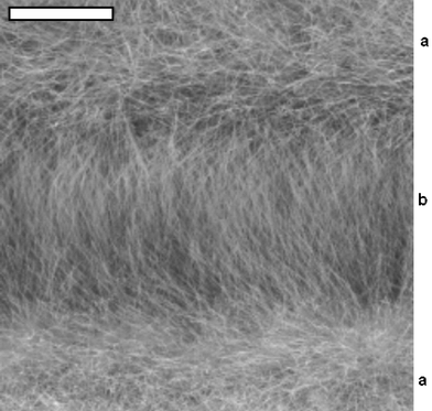 | ||
| Fig. 3 Fibres obtained for deposition in an electric field of 1 V rms at 50 Hz. The scale bar has a width of 20 µm. a, Orientated fibrous growth is obtained in the electrode gap. b, More randomly orientated fibres are observed on the electrode surface. | ||
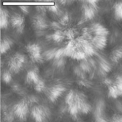 | ||
| Fig. 4 Deposition in an electric field of 10 V rms at 50 Hz. The scale bar has a width of 100 µm. The SEM shows extensive fibrous growth away from the electrode surface, obscuring the electrode pattern beneath. | ||
Variations in reaction conditions
We have studied this system under a variety of different experimental conditions. We have found that deposition of WO3 fibres occurs at a range of deposition temperatures from 400–600 °C. It was decided to concentrate the study at 600 °C as this was the likely maximum operating temperature of the sensor. Gas flow conditions were found to be imperative for film and fibre formation, the gas flow needed to be perpendicular to the substrate; parallel flow produced much less extensive growth. It was presumed that the turbulent flow created by the aerosol gas mixture impacting on the substrate surface encouraged film growth. Extensive fibre growth was observed for a range of gas flow rates and precursor concentration, in particular when the reaction was performed in an external electric field.The gas phase effect of an electric field upon an aerosol
The observed increase in deposited material with applied voltage, whether dc or ac, suggests the presence of a charged precursor aerosol flow. In support of this, a similar amount of material was deposited when varying electric field frequency (10–1000 Hz) at a constant applied voltage (5 V rms). It is expected that with an increase in applied voltage the electric field around the substrate extends further into the aerosol gas stream, thereby attracting a larger volume of aerosol to the sensor surface. Given the lack of a strong permanent dipole across the precursor (W(OPh)6; octahedral) and the use of a relatively non-polar solvent (toluene), the nature of the charge is likely to be static, generated on the surface of the aerosol droplets.The deposition of fibres on the negative electrode at 10 V dc suggests the generation of positively charged droplets. We can say qualitatively that the charge on the aerosols is weak since large electric field strengths (1000–2000 V cm−1) are required for significant localised growth from the surface of the negative electrode, that is, for localisation of deposited material to be dominated by effects of applied voltage effects rather than turbulent gas flow.
The controlling factor in the localisation of material under ac conditions is the electric field frequency. Increasing the ac voltage results in more material being deposited equally on both electrodes, with extended fibres being more evenly distributed across the whole sensor when compared to dc fields. At higher frequency, growth was confined towards the electrode gaps. This can be explained in terms of the time of flight of an aerosol droplet relative to the time period of the ac signal. At sufficiently low frequencies an aerosol droplet is likely to experience only one polarity of electric field during its time of flight and so will tend towards the negative electrode. Therefore, the deposition (5 V rms; 7 V peak voltage) would be more characteristic of high (10 V) voltage dc, but averaged over both electrodes. As the ac frequency increases, a droplet's motion will be influenced by an increasingly alternating field and so will be more localised towards the midpoint of the electrode gap.
Orientation of fibrous growth
Under ac conditions the impedance of WO3−x fibres will be higher than for dc, and so the induced alternating dipole generated in the material is not dissipated. Therefore, the growth will orientate itself with the electric field. Alignment of fibres occurs between the electrodes, where the electric field is strongest. This occurs under all ac conditions. This has parallels to the work of Prasse and Torsten et al.19 who observed structural anisotropy of carbon nanofibres in an epoxy resin dispersion in the presence of an applied ac field. They describe fibre orientation and agglomeration in terms of the electrostatic stabilization afforded to the fibre network by the interacting forces of the external electric field and the electric dipoles induced on the fibres. In our experiments using ac fields, the anisotropic orientation of the fibres is most prominent in the electrode gap, where the field strength is strongest. Morphology more characteristic of radial growth was observed away from the sensor surface, where the weaker electric field lines above the plane of the sensor have a greatly reduced effect on the orientation of fibrous growth. It was at low voltage that we observed growth away from the electrode surface in alignment with the electric field, since at higher voltages the effect was obscured due to the amount of material deposited. A dipole cannot be induced in the fibres under dc because any electric field in the fibre will be dissipated due to the high conductivity of WO3−x, giving rise to random fibre orientation.Gas sensing results
The gas response of a range of morphologies to nitrogen dioxide at 400 °C (90–740 ppb in dry air) is compared to nanoporous, traditionally prepared screen-printed WO3Fig. 5. It is clear that although the applied field can be used to control key factors of film morphology, summarised in Fig. 6, the greatest improvement is for the detection of low concentrations of stable oxidising gases (such as nitrogen dioxide), for example as afforded by deposition of a WO3 film with a bias of 10 V rms (microstructure is shown in Fig. 4).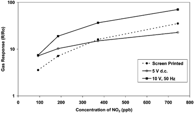 | ||
| Fig. 5 Gas response of tungsten oxide (WO3) sensors prepared by screen-printing and AACVD to nitrogen dioxide. The sensors were tested at 400 °C in dry air to 90, 190, 370 and 740 ppb NO2, using an apparatus of in-house design. | ||
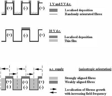 | ||
| Fig. 6 Schematic summary of the effects of applied electric field to film microstructure. The figures show a schematic cross section looking through the sensor. The saw tooth pattern is created by the alternating positive (+) and negative (−) gold electrodes. Top figure shows that at 1 and 5 V dc localised deposition is primarily on the walls of both positive and negative electrodes. At 10 V dc (middle figure) localised deposition is primarily at the top of the negative electrode. For ac deposition (bottom figure) deposition is primarily between the (+)–(−) electrode gap with strongly aligned fibres. | ||
Compared to commercially prepared screen-printed films, we can see that both the solid films deposited at 5 V dc and the extended fibrous material deposited at 10 V rms show significantly larger responses to NO2 below 300 ppb, Fig. 5. The reduced film resistance compared to other films prepared via AACVD (106 Ω for 10 V rms cf. 107–8 Ω for the remaining films) show that there is a larger amount of material deposited between the electrodes (as one would expect at higher bias voltages). However, the reason for increased magnitude of response lies in the increased surface to bulk ratio exhibited by these two films. Depositions at 5 V dc offer comparable solid film thickness to fibre diameters, yet approach saturation at low gas concentrations (ca. 400 ppb) due to significant bulk contributions. Films prepared at 10 V rms utilise all the important features of deposition in an applied electric field, allowing the highest magnitude of response up to 740 ppb. That is, a high volume of extended fibrous growth whose growth aligns with the electric field lines. Compared to lower voltages, the fibres protrude more above the electrode gap, resulting in a less dense material. This allows 3D accessibility to the target gas and so a high surface to bulk ratio. Therefore, a high magnitude of response is maintained over the whole range of gas concentrations. This is only possible due to the growth aligning with field lines, allowing electrical connection above the plane of the sensor.
Conclusion
We have shown that an electric field significantly alters the morphology and orientation of tungsten oxide deposited by AACVD. By controlling the microstructure, producing high surface area fibres that are orientated between the electrodes, we have made a solid-state gas-sensor that is significantly more sensitive than existing commercial sensors for the detection of low concentrations (<700 ppb) of nitrogen dioxide. The use of applied fields in AACVD should be readily applicable to other systems.Acknowledgements
We thank the EPSRC for financial support.References
- P. T. Moseley, A. M. Stoneham and D. E. Williams, in Techniques and Mechanisms in Gas Sensing, ed. P. T. Moseley, J. O. W. Norris and D. E. Williams, Adam Hilger, Bristol, 1991, p. 108 Search PubMed.
- D. E. Williams, in Solid State Gas Sensors, ed. P. T. Moseley and T. C. Tofield, Adam Hilger, Bristol, 1987, p. 46 Search PubMed.
- D. E. Williams and P. T. Moseley, J. Mater. Chem., 1991, 1, 809 RSC.
- D. E. Williams and K. F. E. Pratt, J. Chem. Soc., Faraday Trans., 1998, 94, 3493 RSC.
- S. Kirkpatrick, Rev. Mod. Phys., 1973, 45, 574 CrossRef.
- W. Göpel and K. D. Schierbaum, Sens. Actuators, B, 1995, 26–27, 1 CrossRef.
- D. E. Williams and K. F. E. Pratt, J. Chem. Soc., Faraday Trans., 1998, 94, 3493 RSC.
- D. E. Williams and K. F. E. Pratt, Sens. Actuators, B, 1997, 45, 147 CrossRef.
- G. Chabanis, I. P. Parkin and D. E. Williams, Meas. Sci. Technol., 2003, 14, 76 CrossRef CAS.
- D. E. Williams and K. F. E. Pratt, Sens. Actuators, B, 2000, 70, 214–221 CrossRef.
- G. A. Shaw, K. F. E. Pratt, I. P. Parkin and D. E. Williams, Sens. Actuators, B, 2004, Search PubMed in press.
- D. E. Williams, Sens. Actuators, B., 1999, 57, 1 CrossRef.
- W. B. Cross, I. P. Parkin and K. C. Molloy, Chem. Mater., 2003, 15(14), 2786 CrossRef CAS.
- D. Gogova, K. Gesheva, A. Kakanakova-Georgieva and M. Surtchev, Eur. Phys. J.: Appl Phys, 2000, 11, 167 CrossRef CAS.
- L. Lozzi, L. Ottaviano, M. Passacantando, S. Santucci and C. Cantalini, Thin Solid Films, 2001, 391, 224 CrossRef CAS.
- W. B. Henley and G. J. Sacks, J. Electrochem. Soc., 1997, 144(3), 1045 CAS.
- E. Cazanelli, C. Vinegoni, G. Mariotto, A. Kuzmin and J. Purans, J. Solid State Chem., 1999, 143, 24–32 CrossRef.
- ICDD Powder Diffraction File 20-1324, International Centre for Diffraction Data, Newtown Square, PA, USA Search PubMed.
- L. Prasse, J. Y. Cavaille, P. Torsten and W. Brauher, Compos. Sci. Technol., 2003, 63(13), 1835 CrossRef.
| This journal is © The Royal Society of Chemistry 2005 |