Conductive thin films of θ-(BETS)4[Fe(CN)5NO] on silicon electrodes – new perspectives on charge transfer salts
Luca
Pilia†
a,
Isabelle
Malfant
*a,
Dominique
de Caro
a,
François
Senocq
b,
Antoine
Zwick
c and
Lydie
Valade
a
aLaboratoire de Chimie de Coordination (CNRS UPR 8241), CNRS, 205, route de Narbonne, 31077, Toulouse cedex 4, France. E-mail: malfant@lcc-toulouse.fr; Fax: +33 (0)5-61-55-30-03; Tel: +33 (0)5-61-33-31-06
bENSIACET-CIRIMAT (CNRS UMR 5085), 118, route de Narbonne, 31062, Toulouse cedex 4, France. E-mail: Francois.Senocq@ensiacet.fr
cLaboratoire de Physique des Solides (CNRS UMR 5477), Université Paul Sabatier, 118, route de Narbonne, 31062, Toulouse cedex 4, France. E-mail: Antoine.Zwick@lpst.ups-tlse.fr
First published on 4th December 2003
Abstract
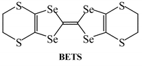
An alternate electrodeposition method using large surface silicon electrodes as anodes to prepare thin films of radical cation salts has been developed. We report on its use for the preparation of the radical cation salt containing the BETS molecule [BETS![[thin space (1/6-em)]](https://www.rsc.org/images/entities/char_2009.gif) =bis(ethylenedithio)tetraselenafulvalene] and the photochromic nitroprusside [Fe(CN)5NO]2− anion, i.e.
θ-(BETS)4[Fe(CN)5NO]. The use of various techniques, such as SEM/EDX, XPS, X-ray, IR and Raman, unambiguously confirmed that the film is made of the θ-(BETS)4[Fe(CN)5NO] phase previously obtained as single crystals on platinum electrodes. These results show that it is possible to electrodeposit cation radical salts on silicon wafers. In addition, this new method of electrodeposition proves to be extremely useful for preparing the large amounts of product (several hundreds of milligrams) often required for physical measurements.
=bis(ethylenedithio)tetraselenafulvalene] and the photochromic nitroprusside [Fe(CN)5NO]2− anion, i.e.
θ-(BETS)4[Fe(CN)5NO]. The use of various techniques, such as SEM/EDX, XPS, X-ray, IR and Raman, unambiguously confirmed that the film is made of the θ-(BETS)4[Fe(CN)5NO] phase previously obtained as single crystals on platinum electrodes. These results show that it is possible to electrodeposit cation radical salts on silicon wafers. In addition, this new method of electrodeposition proves to be extremely useful for preparing the large amounts of product (several hundreds of milligrams) often required for physical measurements.
Introduction
A recent development in the research on molecular conductors concerns the possibility to create solids in which conductivity (or superconductivity) coexists with other physical phenomena.1–3 An approach involving conducting radical cation salts with photochromic anions has been recently explored.4–6 The interest of new molecular conductors containing photochromic anions resides in the influence of the electronic excitation of the anions over the conducting (superconducting) electrons. For example, one can imagine the design of a photochromic molecular conductor (or even a superconductor) in which the conducting properties can be tuned by light. Moreover, the preparation of these materials as thin films is of high interest for potential device application. Light-emitting diodes, nonlinear optical materials and field-effect transistors are a few examples of reported devices using thin organic film technology.7 Much effort is currently being devoted to the processing of thin films of molecule-based materials via thermal evaporation under high vacuum,8,9 chemical vapour deposition,10,11 dip-coating12 or Langmuir–Blodgett techniques.13 However, these procedures have several limitations. In particular, they cannot be used when an electrochemical process is involved. In this context, Wang et al. have recently reported a new approach to the preparation of films of charge transfer salts such as (BEDT)2PF6 [BEDT=bis(ethylenedithio)tetrathiafulvalene] using a gold electrode (surface: 0.5 cm2).14 Moreover, preparation of thin single crystals by confined electrocrystallisation has also been published.15
In parallel, we have developed an alternate electrodeposition method using large surface silicon electrodes as anodes to prepare thin films of radical cation salts. Intrinsic-type silicon wafers have a high enough conductivity (10−3 S cm−1) to be used as electrodes. Doped-type silicon wafers can also be used as they may be of interest for specific applications. As large surface electrodes are concerned, the use of silicon affords evident benefits versus platinum or gold in terms of maintenance and cost. Moreover, galvanostatic electrodeposition allows control of the deposited thickness, which mainly depends on electrolysis duration. Therefore, we considered two different goals: (i) growth of a thin film and (ii) large scale preparation. The first goal is of interest for future applications, silicon still being the substrate of choice in the electronic world for many years to come. The second goal is extremely useful to prepare the large amounts of product (several hundreds of milligrams) often required for physical measurements, when electrolysis is the only possible synthetic route. We illustrate this new application of silicon wafers in the case of the preparation of the radical cation salt containing the BETS molecule [BETS=bis(ethylenedithio) tetraselenafulvalene] and the photochromic nitroprusside [Fe(CN)5NO]2− anion, that is θ-(BETS)4[Fe(CN)5NO]. This compound is a typical example of molecule-based materials that would benefit from both thin film processing and large scale preparation to explore potential photochromic behaviour. As a matter of fact, when associated with cations such as Na+, the nitroprusside anion is known to exhibit extremely long-lived metastable excited states at low temperatures that can be generated by laser irradiation.16,17 However, in this paper, we will focus on the preparation method and compare the properties of the deposit versus those of the single crystals previously obtained on Pt wire electrodes.6
Experimental
Electrodeposition procedure
Electrodeposition is carried out using an intrinsic silicon (100) (Siltronix) one-face-polished wafer (diameter 5 cm, thickness 275 µm) as anode and a platinum wire as cathode. The silicon wafer is stripped in a NH4F–HF solution (12.5% HF 50% and 87.5% NH4F 40%) then washed in distilled water before use. Cleaning of the cathode is performed by treatment with aqua regia, followed by successive anodic and cathodic polarisation of the electrode in dilute sulfuric acid.(PPh4)2[Fe(CN)5NO] is obtained by reaction of Na2[Fe(CN)5NO] (Aldrich) with (PPh4)Cl in water. BETS is prepared as previously reported.18
Solutions of BETS (62 mg) and (PPh4)2[Fe(CN)5NO]
(520 mg) in 1,1,2-trichloroethane (230 mL)–ethanol (22 mL) are introduced into a Schlenk-type cylindrical one-compartment (400 ml) electrochemical cell. The solvents are freshly distilled and 1,1,2-trichloroethane is further run through Al2O3. The galvanostatic oxidation of the donor is performed at 25°C and at a current density of 0.1 µA cm−2. Within 2 days, microcrystals are observable and grow homogeneously on the silicon electrode. A 1 µm thin film is obtained after typically 7 days of electrolysis. When the electrolysis is conducted for 4 weeks on a silicon surface (diameter 5 cm), typically 60 mg of product can be collected by scratching the substrate using a glass slide.
Characterisation methods
Infrared spectra are obtained on powder (scratched from the Si surface) dispersed in KBr matrix, using a Perkin–Elmer Spectrum GX spectrophotometer. Raman measurements are carried out at room temperature with a Raman spectrometer (DILOR XY micro Raman) equipped with a Kr laser (λ=6472 Å, laser power density: 5×10⁴ W cm−2). XPS spectra were recorded using a VG Escalab Model MK2 spectrophotometer (Mg Kα radiation: 1253.6 eV). The SEM images are obtained on a JEOL model JSM 840A.
The X-Ray diffraction studies were performed both on the single crystal powder and film/substrate composite. XRD data were collected with a Seifert XRD 3000 TT, fitted with a diffracted beam monochromator and using Cu Kα radiation (1.5418 Å). In the case of powder analysis, the diffractometer is in Bragg–Brentano configuration (θ/θ), while it is in grazing incidence configuration (ω=2°) for film analysis. The powder sample is spread on a glass sample holder and the film on the silicon sample is placed on a height adjustable holder.
Conductivity measurements were performed using the standard four-probe method between room temperature and 77 K. Electrical contacts between the gold wires and the film were made by using gold paste. They were drawn parallel to each other and the film morphology allowed a large inter-wire distance (≈1 mm). In order to compare the film conductivity with that of the substrate, the conductivity of the silicon wafer was measured separately and found to be 10−3 S cm−1, as given by the supplier (Siltronix) for intrinsic-type silicon.
Except for the IR investigation, all the characterisations are made on the film on substrate samples.
Results and discussion
Crystals of θ-(BETS)4[Fe(CN)5NO], previously obtained by the electrocrystallisation technique using standard platinum wire electrodes, appear as thick blocks and a few other diamond- and hexagonal-plate shaped phases. The compound behaves as a metal down to ca. 40 K with σRT=10−2 S cm−1. Its crystal and electronic structures have already been reported.6 The same cell parameters were found whatever the morphology of the crystals. Further characterisation under irradiation are under progress, but they are limited by the difficulty of obtaining sufficient amounts of compound. A common electrocrystallisation experiment produces about 3 mg of product. In order to increase the amount of product, we used a 5 cm diameter silicon wafer as the anode and a platinum wire as the cathode. The electrodes were placed in a one-compartment cell containing a solution of the donor and the nitroprusside salt. Within few days, a deposit made up of microcrystals (Fig. 1) formed homogeneously on both the polished and non-polished faces of the silicon electrode.
![θ-(BETS)4[Fe(CN)5NO] deposited on Si substrate.](/image/article/2004/NJ/b308699b/b308699b-f1.gif) | ||
| Fig. 1 θ-(BETS)4[Fe(CN)5NO] deposited on Si substrate. | ||
The sample was washed with ethanol and acetone; the deposit does not spontaneously peel off from the silicon surface. The use of a large surface anode was effective in terms of quantity of product: about 60 mg of product is obtained for each experiment. This quite large amount of product allowed us to use numerous techniques to characterise the film and compare its chemical nature to that of the crystals previously obtained.6
SEM images showed that the deposit uniformly covers the surface of the substrate (Fig. 2). It consists of a thin film made of platelets of irregular shapes but also of diamond- and hexagonal-shaped single crystals as previously evidenced.6 EDX analysis confirmed the presence of S, Se and Fe within the microcrystals.
![SEM image of θ-(BETS)4[Fe(CN)5NO] film on silicon substrate.](/image/article/2004/NJ/b308699b/b308699b-f2.gif) | ||
| Fig. 2 SEM image of θ-(BETS)4[Fe(CN)5NO] film on silicon substrate. | ||
XPS analysis of the films gave atomic S/Se and Fe/N ratios of 1.09 and 0.19, respectively, in very good agreement with the theoretical values in the BETS (ratio 1) and Fe(CN)5NO (ratio 0.17) moieties. A least-squares fit deconvolution with Gaussians of the S 2p signal rendered two components at 163.1 and 164.2 eV, very close to those observed for thin films of TTF derivatives.19 A similar treatment for the N 1s signal gave two components at 397.7 and 398.8 eV (Fig. 3). The first line is attributed to the nitrogen atoms of the cyano ligands whereas the second peak is assigned to the nitrogen atom of the NO ligand. Fe 2p3/2 has a binding energy of 708.6 eV, in agreement with that of FeII or FeIII complexes bearing NO ligands.20
![XPS spectrum of the N(1s) electrons for a θ-(BETS)4[Fe(CN)5NO] thin film on Si substrate.](/image/article/2004/NJ/b308699b/b308699b-f3.gif) | ||
| Fig. 3 XPS spectrum of the N(1s) electrons for a θ-(BETS)4[Fe(CN)5NO] thin film on Si substrate. | ||
The structure of the film and that of a powder obtained by electrocrystallisation on a classical platinum wire electrode were analysed by X-ray powder diffraction at room temperature using Cu Kα radiation. In both cases, the diffraction patterns showed broad peaks, indicative of small particle sizes (Fig. 4). Previous calibration of the diffractometer and application of the Scherrer equation gave a crystallite mean size of ca. 80 Å. In both diagrams, we noticed an extra diffraction line [at 2θ=8.197°, (011) line] due to traces of BETS starting material (this was verified from the XRD diagram of a pure sample of BETS).
![XRD diagrams of θ-(BETS)4[Fe(CN)5NO] as powder (a) and as thin film on Si substrate (b). S: trace of starting material (see text).](/image/article/2004/NJ/b308699b/b308699b-f4.gif) | ||
| Fig. 4 XRD diagrams of θ-(BETS)4[Fe(CN)5NO] as powder (a) and as thin film on Si substrate (b). S: trace of starting material (see text). | ||
In order to compare the cell parameters of the powder sample to those previously found in the single crystal study,6 the data were refined with the Checkcell program.21 The peak broadness (due to the small crystallite size and defocusing grazing configuration of the diffractometer) causes overlapping of the diffraction lines (added to the obvious preferred orientation of the film) and so prevents from getting a highly precise result. In the same C2/c space group determined for the single crystal, the calculated parameters for the film are: a=40.01(5), b=4.205(8), c=11.775(9)
Å, β=97.55(3)° and U=1964(6)
Å3. These are to be compared with: a=40.259(8), b=4.1768(7), c=11.599(2)
Å, β=97.23(2)° and U=1934.9(6)
Å3 obtained in ref. 6. From the powder diagram data, and in the C2/c space group, the calculated parameters are: a=40.44(2), b=4.190(2), c=11.785(5)
Å, β=98.29(3)° and U=1976(2)
Å3. As the single crystal study has been performed at 160 K and the powder and the film ones at room temperature, the slight expansion of the cell (≈42 Å3, 2%) seems quite normal. Even if the film diagram displays a preferential orientation (Fig. 4b), the similarity of the data (same position for the detected diffraction lines in film and powder) indicates that the two samples are identified with the same phase. We can then conclude that the film contains the same θ-(BETS)4[Fe(CN)5NO] phase as the single crystal previously studied.
The infrared spectrum of crystals collected from the silicon electrode and dispersed in a KBr matrix evidenced two absorptions at 2963 and 2924 cm−1, identified as the CH2 stretching modes. In the 2100–2200 cm−1 range, two bands are present (2144 and 2134 cm−1), which are assigned to the νCN stretching vibrations. The presence of the NO ligand is confirmed by a νNO absorption at 1941 cm−1
(Fig. 5). In the 1200–1500 cm−1 range, a triplet of bands is observed (1454, 1351 and 1261 cm−1). A similar triplet, assigned to the coupling of the C![[double bond, length as m-dash]](https://www.rsc.org/images/entities/char_e001.gif) C vibrations with the conduction electrons, has been evidenced for κ-(BETS)2FeCl4.22
C vibrations with the conduction electrons, has been evidenced for κ-(BETS)2FeCl4.22
![IR spectrum of θ-(BETS)4[Fe(CN)5NO] thin film (νCN and νNO region).](/image/article/2004/NJ/b308699b/b308699b-f5.gif) | ||
| Fig. 5 IR spectrum of θ-(BETS)4[Fe(CN)5NO] thin film (νCN and νNO region). | ||
Raman spectra were recorded at VV polarisation after focusing the incident laser beam onto the deposit through the microscope objective, giving a spot size of 1 µm2. No major degradation of the sample was observed. The data confirmed the presence of both the BETS and Fe(CN)5NO moieties within the deposit. The spectrum is dominated by a strong broad signal centred at 1470 cm−1
(Fig. 6), which is ascribed to the stretching of the double bonds in the central and peripheral fragments of BETS. For neutral BETS, strong CC modes are observed in the 1490–1530 cm−1 range.22
![Raman spectrum of θ-(BETS)4[Fe(CN)5NO] thin film on Si substrate at room temperature.](/image/article/2004/NJ/b308699b/b308699b-f6.gif) | ||
| Fig. 6 Raman spectrum of θ-(BETS)4[Fe(CN)5NO] thin film on Si substrate at room temperature. | ||
The lower observed CC frequency for the films is in agreement with the cationic character of the BETS moiety. A similar frequency shift due to the charge transfer between donor and acceptor molecules has been observed for thin films of TTF[Ni(dmit)2]2.23 Medium-intensity bands are evidenced at 439, 479 (νFe–C) and 638 (νFe–N) cm−1, assigned by comparison with the Raman spectrum of Na2[Fe(CN)5NO].16 Several medium- or low-intensity features are present in the 800–1000 cm−1 range. They are related to both νC–S and νC–Se stretching modes and to δC–C–S and δS–C–Se deformation modes present in the Raman spectrum of κ-(BETS)2FeCl4.22 Moreover, a weak band at 2134 cm−1 is assigned to the CN vibrational modes. It should be pointed out that the orientation of the microcrystals on the substrate favours the presence of this latter band.
Conductivity has been measured directly on the microcrystalline film grown on the silicon wafer using the standard four-probe technique. The conductivity of the film is about 1.6 S cm−1 at room temperature (Fig. 7), well above that of the Si substrate (10−3 S cm−1). This value shows the high intrinsic conductivity of the material compared to the 10−2 S cm−1 value obtained on a single crystal and the 5×10⁻² S cm−1 measured on the compacted powder. Despite the low conductivity of inter-fiber or inter-grain contacts within the film, the two orders of magnitude variation observed between the crystal and the film is attributed to the fact that the measurement on the single crystal was not performed along the most favourable conductive direction. The shape and the size (0.4×0.2×0.05 mm3) of the crystal did not allow other orientations. In contrast, the microcrystals seem to grow on the silicon wafer in a favourable orientation versus the substrate plane. Moreover, the semiconductive thermal behaviour (Ea=0.03 eV) compared to the metallic one observed in the single crystal means that the overall electric behaviour of the material is affected by the inter-grain contacts. This has been already observed in films of TTF–TCNQ.24
![Conductivity of θ-(BETS)4[Fe(CN)5NO] thin film on Si substrate as a function of temperature.](/image/article/2004/NJ/b308699b/b308699b-f7.gif) | ||
| Fig. 7 Conductivity of θ-(BETS)4[Fe(CN)5NO] thin film on Si substrate as a function of temperature. | ||
Conclusion
We have reported on the use of silicon wafers as electrodes to grow thin films of molecule-based materials by electrodeposition. This is illustrated in the case of the preparation and characterisation of a BETS-based radical cation salt containing the photochromic nitroprusside anion, obtained as an adherent thin film on a silicon wafer. The use of various techniques, as SEM/EDX, XPS, X-Ray, IR and Raman, unambiguously confirmed that the film is made of the θ-(BETS)4[Fe(CN)5NO] phase previously obtained as single crystals on platinum electrodes. These results show that it is possible to electrodeposit cation radical salts on silicon wafers. In addition, this new method of electrodeposition proved to be extremely useful for preparing the large amounts of product (several hundreds of milligrams) often required for physical measurements. This method can be extended to other molecular systems. Growth and characterisation of other kinds of films are in progress.Acknowledgements
This research was supported through a European Community Marie Curie Fellowship (Contract HPMT CT2001 00398) for L. P. Partial support from the COST D14/003/99 program is acknowledged. The authors gratefully thank C. Faulmann for conductivity measurements, M. Reversat (ENSiACET, Toulouse) for SEM experiments and G. Chatainier (ENSiACET, Toulouse) for XPS results.References
- M. Kurmoo, A. W. Graham, P. Day, S. J. Coles, M. B. Hursthouse, J. L. Caulfield, J. Singleton, F. L. Pratt, W. Hayes, L. Ducasse and P. Guionneau, J. Am. Chem. Soc., 1995, 117, 12209 CAS.
- H. Kobayashi, A. Kobayashi and P. Cassoux, Chem. Soc. Rev., 2000, 29, 325 RSC.
- E. Coronado, J. R. Galan-Mascaros, C. J. Gomez-Garcia and V. Laukhin, Nature (London), 2000, 447 CrossRef CAS.
- M. Gener, E. Canadell, S. S. Khasanov, L. V. Zorina, R. P. Shibaeva, L. A. Kushch and E. B. Yagubskii, Solid State Commun., 1999, 111, 329 CrossRef CAS.
- L. V. Zorina, S. S. Khasanov, R. P. Shibaeva, M. Gener, R. Rousseau, E. Canadell, L. A. Kushch, E. B. Yagubskii, O. O. Drozdova and K. Yakushi, J. Mater. Chem., 2000, 10, 2017 RSC.
- M.-E. Sanchez, M.-L. Doublet, C. Faulmann, I. Malfant, P. Cassoux, L. A. Kushch and E. B. Yagubskii, Eur. J. Inorg. Chem., 2001, 2797 CrossRef CAS.
- J. Fraxedas, Adv. Mater., 2002, 14, 1603 CrossRef CAS and references herein.
- S. Molas, J. Caro, J. Santiso, A. Figueras, J. Fraxedas, C. Méziére, M. Fourmigué and P. Batail, J. Cryst. Growth, 2000, 218, 399 CrossRef CAS.
- K. Kawabata, K. Tanaka and M. Mizutani, Solid State Commun., 1991, 74, 83 CrossRef CAS.
- J. Caro, J. Fraxedas and A. Figueras, Chem. Vap. Deposition, 1997, 3, 263 CAS.
- D. de Caro, M. Basso-Bert, J. Sakah, H. Casellas, J.-P. Legros, L. Valade and P. Cassoux, Chem. Mater., 2000, 12, 587 CrossRef CAS.
- D. de Caro, J. Sakah, M. Basso-Bert, C. Faulmann, J.-P. Legros, T. Ondarçuhu, C. Joachim, L. Ariès, L. Valade and P. Cassoux, C. R. Acad. Sci., Ser. IIc: Chim., 2000, 3, 675 CrossRef CAS.
- T. Bjornholm, T. Hassenkam and N. Reitzel, J. Mater. Chem., 1999, 9, 1975 RSC.
- H. H. Wang, K. L. Stamm, J. P. Parakka and C. Y. Han, Adv. Mater., 2002, 14, 1193 CrossRef CAS.
- (a) P. Batail, K. Boubekeur, M. Fourmigué and J.-C. P. Gabriel, Chem. Mater., 1998, 10, 3005 CrossRef CAS; (b) A. Deluzet, S. Perruchas, H. Bengel, P. Batail, S. Molas and J. Fraxedas, Adv. Funct. Mater., 2002, 12, 123 CrossRef CAS.
- Th. Woike, W. Krasser, P. S. Bechthold and S. Haussühl, Solid State Commun., 1983, 45, 499 CrossRef CAS.
- M. D. Carducci, M. R. Pressprich and P. Coppens, J. Am. Chem. Soc., 1997, 119, 2669 CrossRef CAS.
- T. Courcet, I. Malfant, K. Pokhodnia and P. Cassoux, New J. Chem., 1998, 6, 585 RSC.
- J. Fraxedas, J. Caro, A. Figueras, P. Gorostiza and F. Sanz, J. Vac. Sci. Technol., A, 1998, 16, 2517 CrossRef CAS; H. Casellas, D. de Caro, L. Valade and J. Fraxedas, New J. Chem., 2002, 26, 915 RSC.
- S. A. Best, P. Brant, R. D. Feltham, T. R. Rauchfuss, D. M. Roundhill and R. A. Walton, Inorg. Chem., 1976, 16, 1977.
- The Checkcell program was developed by J. Laugier and B. Bochu, and can be downloaded from: http:/www.ccp14.ac.uk/tutorial/lmgp.
- I. Olejniczak, A. Graja, N. D. Kushch, P. Cassoux and H. Kobayashi, J. Phys. I, 1996, 6, 1631 Search PubMed.
- L. Valade, H. Casellas, S. Roques, C. Faulmann, D. de Caro, A. Zwick and L. Ariès, J. Solid State Chem., 2002, 168, 438 CrossRef CAS.
- P. Chaudhari, B. A. Scott, R. B. Laibowitz, Y. Tomkiewicz and J. B. Torrance, Appl. Phys. Lett., 1974, 24, 439 CAS.
Footnote |
| † Present address: Dipartimento di Chimica Inorganica ed Analitica, Università degli Studi di Cagliari, S.S. 554 bivio per Sestu, I-09042 Monserrato (Cagliari), Italy |
| This journal is © The Royal Society of Chemistry and the Centre National de la Recherche Scientifique 2004 |