Enhanced hole injection in organic light-emitting diodes using a SAM-derivatised ultra-thin gold anode supported on ITO glass
Ross A.
Hatton
*a,
Martin R.
Willis
a,
Michael A.
Chesters
a,
Frank J. M.
Rutten
b and
David
Briggs
b
aSchool of Chemistry, University of Nottingham, Nottingham, UK NG7 2RD. E-mail: pcxrah@unix.ccc.nottingham.ac.uk
bCentre for Surface Chemical Analysis, University of Nottingham, Nottingham, UK NG7 2RD
First published on 12th November 2002
Abstract
In order to increase the performance of organic light-emitting diodes (OLEDs) we report the modification of the indium-tin oxide (ITO) anode invariably used in OLEDs, with a dipolar self-assembled monolayer-derivatised (4-nitrophenylthiolate) ultra-thin gold overlayer. This composite approach allows the work function of the anode to be tuned to the hole-transporting band of the adjacent semiconductor, while facilitating good mechanical adhesion at this interface. When this modification is incorporated into the model OLED system ITO/TPD/Alq3/C6H5CO2Li/Al [where TPD is N,N′-bis(3-methylphenyl)-N,N-diphenyl-1,1-biphenyl-4,4′-diamine, Alq3 is tris(quinolin-8-olato)aluminium and C6H5CO2Li is lithium benzoate], the power efficiency is dramatically enhanced. Furthermore, these devices exhibit a maximum external quantum efficiency of more than 5 cd A−1 and a peak luminance of ∼36,000 cd m−2. In combination with the current–voltage–luminance (LIV) characterisation of these devices, scanning Kelvin probe, polarisation modulation reflection absorption infrared spectroscopy and time of flight secondary ion mass spectroscopic techniques have been employed to probe the ITO–Au–SAM interface. This research builds on our earlier work with dipolar organosilanes, phosphonic acids and charge-transfer films at the ITO–organic interface.
1 Introduction
Both polymer and molecular thin film organic light-emitting diodes (OLEDs) are now sufficiently well developed to be commercially exploited as the basis for flat panel displays. However, there remains interest in reducing the operating voltage so that further improvements can be made in power efficiency, compatibility with conventional integrated circuitry and device lifetime.Thin films of indium tin oxide (ITO) supported on a glass substrate are invariably employed as the anode in OLEDs due to their high transparency over the visible region (80–90%), electrical conductivity (<80 Ω □−1) and relatively high work function (4–5 eV).1 Unfortunately, these properties are highly sensitive to the method of preparation and so there can be considerable variations between glass supplied by different manufacturers, particularly in the work function.2 In order to achieve efficient hole injection from the anode, its Fermi level must be aligned with the highest occupied molecular orbital (HOMO) of the adjacent organic film. However, the work function of ITO is generally not sufficiently large for the contact to be Ohmic and so there is a barrier to carrier injection. Furthermore, the almost metallic conductivity of ITO at room temperature is afforded by the high density of naturally occurring defect and dopant states within, and just below the conduction band.3 Consequently, the amorphous oxide surface is chemically ill-defined and is believed to be a source of metal ions and other impurities, which diffuse into the active organic layers under operation, to the detriment of device performance.4–6
In response to these problems, the ITO anode has been modified with both thin films7–9 and self-assembled monolayers (SAMs)6,10–16 to reduce the barrier to hole injection, improve adhesion at the anode–organic film interface17,18 and inhibit possible diffusion of material across the interface. SAMs of dipolar acids10–12,14,15 and, more recently, covalently bound silanes,16 have proven to be an effective means of tuning the work function of the ITO anode for use in OLEDs. In these cases, the dipolar SAM essentially behaves as an artificial electrical double layer, modifying the electrostatic conditions at the oxide surface. The resulting change in work function is dependent on the size and orientation of the permanent molecular dipole relative to the electrode surface, the nature of the bonding interaction with the surface and the SAM packing density.14,15,19 We believe that, in the context of organic light-emitting diodes, covalently bound silane SAMs represent the most promising approach to monolayer derivatisation of ITO, owing to the stability of the siloxane linkage with the electrode surface. However, whilst dipolar SAMs are an effective means of modifying the work function of ITO glass, they do nothing to reduce the variability in the work function of ITO glass supplied by different manufacturers.
It is well documented that both the conductivity and visual transparency of noble metal films is significantly enhanced when prepared on certain metal oxide surfaces,20 as compared to the same films on silica. However attempts by Tadayyon et al.21 to induce favourable increases in the work function of ITO using gold overlayers proved troublesome, since the ultra-thin overlayers seemed to be particularly reactive to impurities, even under ultra-high vacuum conditions. Platinum films were found to be less problematic in this respect, indeed, discontinuous Pt films on ITO have recently been found to be a simple way to enhance the performance of the ITO anode.22
This study describes a composite approach, which involves modification of the ITO anode with a dipolar SAM-passivated (4-nitrophenylthiolate) ultra-thin gold overlayer. In this way, the work function of the anode may be tailored for use in a given OLED construction, whilst separating the active organic layers from the impure oxide surface (Fig. 1). Whilst it is desirable that the gold films are continuous, a low electrical resistance is not required, and so ultra-thin films may be utilised, thus minimising the expected loss in anode transparency. Relative work function measurements, obtained using a scanning Kelvin probe (SKP), combined with a semi-quantitative investigation into surface composition, undertaken using time of flight secondary ion mass spectroscopy (ToF-SIMS), reveal that, for a deposited gold thickness of 40 Å, coverage of the ITO substrate by the gold overlayer exceeds 80%. When derivatised with a 4-nitrophenylthiolate SAM, the work function of this electrode is comparable with that of a gold reference electrode derivatised with the same SAM. The anode work function, and hence the barrier to carrier injection, is therefore only weakly dependent on the work function of the underlying ITO. Polarisation modulation reflection absorption infrared spectroscopy (PM-RAIRS) has also been successfully applied to give complementary information on the orientation of the SAM at the electrode surface. Using the model OLED system ITO/TPD/Alq3/C6H5CO2Li/Al [where TPD is N,N′-bis(3-methylphenyl)-N,N′-diphenyl-1,1′-biphenyl-4,4′-diamine, Alq3 is tris(quinolin-8-olato)aluminium and C6H5CO2Li is lithium benzoate], current–voltage, luminance–voltage and external quantum efficiency data are used to compare the performance of a modified device to that of a reference.
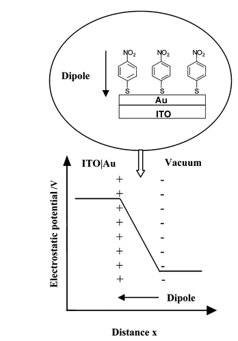 | ||
| Fig. 1 Schematic of the variation in electrostatic potential across the surface dipolar layer, acting to increase the work function of the underlying ITO–Au. | ||
2 Experimental
2.1 Device fabrication
All glassware was thoroughly cleaned and dried prior to use. The ITO-coated glass (100 nm ITO with a SiO2 barrier on 1.1 mm soda lime glass substrate with a sheet resistance of 20 Ω □−1) was purchased from Merck and cut into 25 × 20 mm slides. Each slide was swabbed with acetone, followed by a sequence of 30 min ultrasonic baths in toluene, detergent (Decon-90) in nano-pure water, and finally, in analytical grade acetone. Immediately before use, the substrates were immersed in hot acetone vapour.The gold films were deposited at rate of 0.2 Å s−1 from a shielded thermal source 14 cm from the substrate at room temperature. The deposited thickness was measured using an Edwards quartz crystal microbalance mounted adjacent to the substrate and has an associated error of ±10%. Immediately after deposition of the gold overlayer, the substrates were removed from the vacuum and submerged in a 1 × 10⁻³ M solution of 4-nitrophenylthiol (NPT) in dichloromethane for 20 h at room temperature.19 SAMs of dipolar molecules can be stabilised by interaction with a polar solvent23 and so, to facilitate the formation of dense NPT SAMs, dichloromethane was used. The 4-nitrophenylthiol (95% purity) was obtained from Acros, stored at 4 °C and used without further purification. Upon removal from the thiol solution, the substrate was rinsed with a 30% methanol in chloroform solution and dried in a stream of dry nitrogen.
The bilayer OLEDs were fabricated in a modified Edwards auto-306 vacuum coating unit, by successive vapour deposition of the organic layers onto ITO-coated glass substrates, followed by the deposition of a patterned aluminium electrode. The ITO substrate etching procedure, along with details of the device testing apparatus, have been documented in a previous publication.14 Each organic layer (500 Å) was vacuum deposited (6 × 10⁻⁶ mbar) at a rate of 2–3 Å s−1 followed by the deposition of the aluminium electrode (500 Å) at 5–10 Å s−1. The current–voltage and luminance–voltage characteristics under forward bias were measured with custom-built apparatus interfaced to a personal computer. Luminance–voltage and current–voltage data points were collected at 5 s intervals and each data point represents the average of five consecutive measurements. Each data set plotted represents the averaged characteristics of three typical devices. Typically, devices had an associated error of less than ±8% for current density and less than ±5% for luminance readings. Unipolar diodes were fabricated in order to assess the hole-injection efficiency from the anode. These devices consisted of a 3000 Å TPD film sandwiched between the anode and an aluminium cathode. All measurements were made in the dark.
2.2 Characterisation
An estimate of the extent of surface coverage by the gold overlayer can be deduced from comparison of the integrated absolute signal intensity of gold ions from the modified substrate with those from a gold reference. The gold reference substrate was a 1000 Å gold film supported on ITO glass. Both substrates were prepared under identical conditions. Alternatively, a measure of the fraction of the ITO support left uncovered by the gold overlayer can be derived from a comparison of the integrated signal intensity of secondary ions characteristic of the ITO support (e.g. InO−) with and without the gold overlayer. Only those peaks which were unaffected by overlaps with other components at the same nominal mass and which had good counting statistics were compared in this way, namely the negative ion clusters Au2−, Au3− and Au4−, and InO− (m/z ∼130.9). A representative sample of these data is given in Fig. 3. In order to be able to compare absolute signal intensities between samples with confidence, the samples for comparison were prepared in the same way, at the same time and mounted identically (side-by-side) in the sample holder. Absolute signal intensities of the ion fragments of interest exhibited less than 5% variation between randomly chosen areas on the same sample.
It is instructive to note that a certain level of hydrocarbon contamination of clean surfaces is inherent in high vacuum systems routinely used for the evaporation of organic material. Indeed, the high surface energy of clean gold substrates favours the adsorption of such contamination, which may affect the secondary ion yield of elemental species. The sputter yield of gold clusters and ITO matrix fragments (e.g. InO− and SnO−) may be less sensitive to surface contamination effects, hence the choice of these species for intensity comparisons. To a first approximation, matrix effects on the sputter yield of ions from the composite surface, as compared to the ITO and gold references, are ignored, since regions of ITO and gold are assumed to be spatially separated. This assumption would be consistent with the island growth mode characteristic of noble metals evaporated onto oxide surfaces.20
Infrared spectra were obtained using a Hinds Photoelastic Modulator-90 and GWC Korn Box interfaced with a Nicolet Nexus-870 FTIR spectrometer. The beam was incident at ∼80° to the surface normal and typically 2048 scans at 4 cm−1 resolution were co-added. The data are presented without baseline correction or smoothing.
3 Discussion and results
3.1 Surface potential/coverage studies
A deposited gold thickness of 40 Å was chosen as an acceptable compromise between substrate transparency and the desire to ensure high coverage of the underlying ITO substrate. The transparency of such a film is typically 70% over the visible spectrum and as high as 82% at 520 nm, which corresponds to the most intense emission wavelength from the Alq3 emitter layer.30 When derivatised with a NPT SAM, the surface contact potential of this substrate is ∼310 mV lower than that of the ITO reference (Fig. 2), corresponding to a ∼310 meV increase in work function. This value is in agreement with the measured increase in work function for the same SAM on a gold reference, suggesting high surface coverage of the ITO support by the gold overlayer. To verify this conclusion, static SIMS was applied to probe the surface chemistry. This technique is non-destructive over the duration of the experiment and surface specific.24 A comparison of absolute secondary ion intensities for fragment ions characteristic of the gold overlayer on ITO with those from gold and ITO references (namely InO−, Au2−, Au3− and Au4−) provides a simple measure of the extent of surface heterogeneity (Fig. 3). The ratio of the InO− peak intensity from the gold-modified ITO surface to that from an ITO reference was 0.03. The ratios of the Au2−, Au3− and Au4− peak intensities to those from a gold reference were 0.79, 0.90 and 0.85, respectively. If it is assumed that the gold overlayer on the ITO substrate is formed according to an island growth mode, then at high gold coverage, InO− fragments will originate only from narrow cracks between adjacent gold islands tens of ångströms in height. This topography is expected to hinder the production of secondary ions from areas of exposed ITO and offers a possible explanation for the anomalously high surface coverage deduced from the InO− ion intensities (97%). It is therefore concluded that the fraction of the ITO support covered by the 40 Å gold overlayer is between 80 and 90%. | ||
| Fig. 2 Surface potential profiles relative to ITO of NPT SAM-passivated Au supported on ITO substrates: (○) 40 Å overlayer; (●) 500 Å film. | ||
 | ||
| Fig. 3 Portions of the negative ion ToF-SIMS spectra from (a) a 40 Å Au overlayer on ITO (solid line) and the 1000 Å Au film reference (broken line), and (b) a 40 Å Au overlayer on ITO (solid line) and the ITO reference (broken line). | ||
3.2 PM-RAIRS studies
The PM-RAIRS spectra shown in Fig. 4 provide direct evidence for the presence of the NPT SAM on the gold-modified ITO substrate. The good correlation between the monolayer spectra in Fig. 4(a) and (b) supports the assumption that the reflection properties of the ITO glass used during the course of this investigation can be approximated to those of a highly reflecting metallic substrate over the spectral range of interest. The PM-RAIRS spectra from the gold-modified ITO substrate include a broad absorption at approximately 1250 cm−1, which modifies the baseline at the low frequency end of the spectral range shown in Fig. 4(a), as compared to the same spectra from the gold reference substrate [Fig. 4(b)]. This absorption is characteristic of the longitudinal optical mode (Si–O–Si asymmetric stretching mode) of the glass substrate beneath the ITO film.28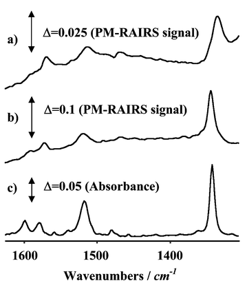 | ||
| Fig. 4 PM-RAIRS spectra of NPT SAM-passivated Au supported on ITO substrates: (a) 40 Å overlayer; (b) 1000 Å reference film. (c) IR transmission spectrum of NPT in chloroform. | ||
The two strong bands around 1350 and 1525 cm−1 are characteristic of the symmetric and antisymmetric vibrational modes of a nitro moiety with conjugation to an aromatic ring.31–33 The antisymmetric stretch is normal to the 1,4 molecular axis, along which the transition dipole moment of the symmetric stretch is orientated. Around 1600 and 1580 cm−1 is a doublet characteristic of the aromatic ring, which is relatively intense owing to the large dipole moment change produced by movements of the 1,4 ring substituents. The band at 1580 cm−1 is usually very much weaker than that at 1600 cm−1,31 but is enhanced in this case owing to the high degree of conjugation in the molecule and the presence of the nitrogen lone pair. The transition dipole moment of this vibration is normal to the 1,4 molecular axis and in the plane of the ring, unlike that at 1600 cm−1, which is parallel to the 1,4 axis. Since vibrational modes both parallel and normal to the 1,4 molecular axis are present in the spectra, the NPT molecules are neither upright nor flat on the surface, but at some intermediate angle. As a result, the maximum theoretical increase in electrode work function for this SAM on gold is not achieved, as this would correspond to the 1,4 molecular axis orientated normal to the plane of the electrode surface.
The relative intensities of the pair of bands assigned to ring stretching, and of the pair of bands assigned to the symmetric and antisymmetric stretching of the nitro group, should each provide a marker for the orientation of the molecular axis with respect to the surface normal. The different behaviour of the relative intensities of these pairs of bands indicates that the nitro group is rotated out of the plane of the phenyl ring, as is known to occur in some crystal structures. Similar behaviour has recently been reported by Hinrichs et al. for a Langmuir–Blodgett film of nitrophenyl-substituted 2,5-diphenyl-1,3,4-oxadiazole.34 However, the extent of the reversal in the relative intensities of the 1600 and 1580 cm−1 bands in the monolayer spectra in Fig. 4(a) and (b), combined with their shift to lower frequencies as compared to the corresponding peaks in solution [Fig. 4(c)], indicate that these intensity changes are not purely orientational effects. We suggest that these effects are evidence for the chemical interaction of the thiol moiety with the gold surface in the SAM, since both the intensities and frequencies of these aromatic ring vibrational modes are highly dependent on the nature of the 1,4 ring substituents.31
3.3 Current–voltage characterisation
Ideally the hole-flow regime across the anode–TPD interface is Ohmic and so the current density supplied is governed by the intrinsic transport properties of the TPD bulk. This condition is described as the space charge-limited current (SCLC) flow regime. Since glassy, evaporated TPD is known to be essentially trap free (TF),35 the TF-SCLC is given by the Mott-Gurney law,| JTF-SCLC = (9/8)εε0μ(V2/d3) | (1) |
 | ||
| Fig. 5 Forward bias log-linear current density–voltage characteristics for the diode construction anode/3000 Å TPD/Al at 293 K. Anode = ITO (○), ITO/40 Å Au/NPT (●); Ohmic contact (-). | ||
3.4 Device studies
When the ITO anode in the device structure ITO/TPD/Alq3/Al is replaced with the Au–SAM-modified ITO electrode, the injected current density is dramatically enhanced (Fig. 6), shifting the luminance–voltage profile to lower voltages by 5.5 V (Fig. 7). Whilst this effect obviously benefits the power efficiency of the device, the effect on the recombination, or quantum, efficiency is more difficult to predict. A possible explanation for the observed changes in quantum efficiency (Fig. 8) can be given within the context of a model originally proposed by Khramtchenkov et al.37,38 The model predicts that the electron and hole densities within the recombination zone are maintained by the beneficial effect that the accumulation of majority carriers at the TPD–Alq3 interface has on the number of minority carriers injected into the device. If, for example, the barrier to hole injection is smaller than that to electron injection, there will be an accumulation of holes at the TPD–Alq3 interface, which acts to redistribute the internal electric field within the device, focusing it over the Alq3 layer. Consequently, hole injection from the anode is reduced and electron injection from the cathode is increased, which acts to maintain balanced charge densities within the recombination zone. However, this beneficial feedback mechanism is only operative for moderate field strengths and when the barriers to electron and hole injection are not dramatically different. At low electric field strengths, the concentration of carriers is so low that they are swept away before radiative recombination events can occur, while at the other extreme, field-assisted leakage currents across the device reduce efficiency. From a consideration of the energy levels within the ITO/TPD/Alq3/Al system, the barrier to electron injection is much larger than for hole injection from the ITO anode. Under these circumstances, the electric field focused across the Alq3 layer is so great that field-assisted hole migration to the cathode becomes significant. This is consistent with the relatively low quantum efficiencies for both devices employing an aluminium cathode. One possible explanation for the small increase in quantum efficiency upon incorporation of the Au–SAM-modified anode into this device is the expected reduction in field-induced dissociation of exitons within the emission zone resulting from the dramatically reduced operating voltage.39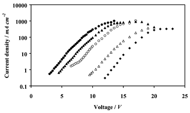 | ||
| Fig. 6 Current–voltage characteristics: (Δ) ITO/TPD/Alq3/Al; (▲) ITO/40 Å Au/NPT/TPD/Alq3/Al; (○) ITO/TPD/Alq3/C6H5CO2Li/Al; (●) ITO/40 Å Au/NPT/TPD/Alq3/C6H5CO2Li/Al; (◆) ITO/40 Å Au/TPD/Alq3/Al. | ||
 | ||
| Fig. 7 Luminance–voltage plots: (Δ) ITO/TPD/Alq3/Al; (▲) ITO/40 Å Au/NPT/TPD/Alq3/Al; (○) ITO/TPD/Alq3/C6H5CO2Li/Al; (●) ITO/40 Å Au/NPT/TPD/Alq3/C6H5CO2Li/Al; (◆) ITO/40 Å Au/TPD/Alq3/Al. | ||
 | ||
| Fig. 8 External quantum efficiency–voltage plots: (Δ) ITO/TPD/Alq3/Al; (▲) ITO/40 Å Au/NPT/TPD/Alq3/Al; (○) ITO/TPD/Alq3/C6H5CO2Li/Al; (●) ITO/40 Å Au/NPT/TPD/Alq3/C6H5CO2Li/Al. | ||
In an attempt to rectify the imbalance between the barrier to electron and hole injection in those bilayer OLEDs employing an aluminium cathode, the barrier to electron injection was reduced via the incorporation of a lithium benzoate interlayer at the aluminium–Alq3 interface. As is clear from Fig. 8 that this dramatically enhances the carrier recombination efficiency, suggesting that the barrier to electron injection is well matched to that from the anode. Under these conditions, the reduction in the height of the barrier to hole injection with the modified ITO anode as compared to bare ITO can be compensated for by the self-correcting mechanism predicted to occur at moderate field strengths by Khramtchenkov et al.37,38 This description is consistent with the absence of any change in form of the quantum efficiency curve as a function of drive voltage. As is clear from Fig. 7 and 8, devices incorporating the Au–SAM-modified ITO anode coupled with the lithium benzoate-modified aluminium cathode have external quantum efficiencies greater than 3 cd A−1 over the luminance range between 600 and 36![[thin space (1/6-em)]](https://www.rsc.org/images/entities/char_2009.gif) 000 cd m−2. Furthermore, the drive voltage at 100, 300 and 1000 cd m−2 are 5.0, 5.8 and 6.75 V, respectively, which represents a considerable improvement over the reference devices.
000 cd m−2. Furthermore, the drive voltage at 100, 300 and 1000 cd m−2 are 5.0, 5.8 and 6.75 V, respectively, which represents a considerable improvement over the reference devices.
The poor performance of the OLED incorporating a gold overlayer-modified ITO anode without a NPT SAM (Fig. 6 and 7), implies a large barrier to hole injection. This is because TPD molecules at the surface of gold are known to be perturbed by the surface potential in such a way as to induce an abrupt negative vacuum level shift exceeding 1 eV.40 Consequently, despite the favourably high work function of bare gold, the barrier to hole injection across the Au–TPD interface is large. Abrupt vacuum level shifts at the interface between some metals and non-polar organic films almost always act to reduce the work function of the underlying metal. Ishii et al.1 suggest that this effect is often wrongly attributed to charge transfer, pointing out that the mirror force (or image effect) and/or rearrangement of the electron cloud at a metal surface in the presence of a physically absorbed overlayer (or push back effect), can also result in a negative vacuum level shift.
4 Conclusion
This work has shown that ITO glass, which is invariably employed as the anode in OLEDs, can be modified with an ultra-thin, SAM-derivatised, gold overlayer as a means of fabricating an anode with a tunable work function. When a 4-nitrophenylthiolate SAM-derivatised 40 Å Au overlayer-modified ITO substrate was employed as the anode in the model OLED anode/TPD/Alq3/C6H5CO2Li/Al, a peak external quantum efficiency of 5.20 cd A−1, combined with low operating voltage, was achieved. An ITO substrate modified in this way is amenable to detailed spectroscopic investigation using the grazing angle infrared technique PM-RAIRS, whilst being sufficiently transparent over the visible spectrum for use in OLEDs.Acknowledgements
The authors would like to thank Mel Beasley for technical support, and the EPSRC for funding this research.References
- H. Ishii, K. Sugiyama, E. Ito and K. Seki, Adv. Mater., 1999, 11(8), 605–625 CrossRef CAS.
- H. Antoniadis, J. N. Miller, D. B. Roitman and I. H. Campbell, IEEE Trans. Electron Devices, 1997, 44(8), 1289–1294 CrossRef CAS.
- R. B. H. Tahar, T. Ban, Y. Ohya and Y. Takahashi, J. Appl. Phys., 1998, 83(5), 2631–1294 CrossRef.
- J. C. Scott, J. H. Kaufman, P. J. Brock, R. DiPietro, J. Salem and J. A. Goitia, J. Appl. Phys., 1996, 79(5), 2745–2751 CrossRef CAS.
- S. T. Lee, Z. Q. Gao and L. S. Hung, Appl. Phys. Lett., 1999, 75, 1404–1406 CrossRef CAS.
- K. W. Wong, H. L. Yip, Y. Luo, K. Y. Wong, W. M. Lau, K. H. Low, H. F. Chow, Z. Q. Gao, W. L. Yeung and C. C. Chang, Appl. Phys. Lett., 2002, 80(15), 2788–2790 CrossRef CAS.
- X. M. Ding, L. M. Hung, L. F. Cheng, Z. B. Deng, X. Y. Hou, C. S. Lee and S. T. Lee, Appl. Phys. Lett., 2000, 76(19), 2704–2706 CrossRef CAS.
- W. Hu, K. Manabe, T. Furukawa and M. Matsumura, Appl. Phys. Lett., 2002, 80(15), 2640–2641 CrossRef CAS.
- S. R. Day, R. A. Hatton, M. A. Chesters and M. R. Willis, Thin Solid Films, 2002, 410, 159–166 CrossRef CAS.
- F. Nüesch, L. Si-Ahmed, B. François and L. Zuppiroli, Adv. Mater., 1997, 9(3), 222- CrossRef.
- S. F. J. Appleyard and M. R. Willis, Opt. Mater., 1998, 9, 120–124 CrossRef CAS.
- F. Nüesch, F. Rotzinger, L. Si-Ahmed and L. Zuppiroli, Chem. Phys. Lett., 1998, 288, 861–867 CrossRef CAS.
- P. K. H. Ho, M. Granström, R. H. Friend and N. C. Greenham, Adv. Mater., 1998, 10(10), 769–774 CrossRef CAS.
- S. F. J. Appleyard, S. R. Day, R. D. Pickford and M. R. Willis, J. Mater. Chem., 1999, 10, 169–173 RSC.
- C. Ganzorig, K. Kwak, K. Yagi and M. Fujihira, Appl. Phys. Lett., 2001, 79(2), 272–274 CrossRef CAS.
- R. A. Hatton, S. R. Day, M. A. Chesters and M. R. Willis, Thin Solid Films, 2001, 394, 292–297 CrossRef CAS.
- M. Carrard, S. Goncalves-Conto, L. Si-Ahmed, D. Adès and A. Siove, Thin Solid Films, 1999, 352, 189–194 CrossRef CAS.
- J. Cui, Q. Huang, J. G. C. Veinot, H. Yan and T. J. Marks, Adv. Mater., 2002, 14(8), 565–569 CrossRef CAS.
- R. W. Zehner, B. F. Parsons, R. P. Hsung and L. R. Sita, Langmuir, 1999, 15, 1121–1127 CrossRef CAS.
- L. Holland, Vacuum Deposition of Thin Films, Chapman and Hall, London, 1960 Search PubMed.
- S. M. Tadayyon, K. Griffiths, P. R. Norton, C. Tripp and Z. Popovic, J. Vac. Sci. Technol., A., 1999, 17(4), 1773–1778 CrossRef CAS.
- Y. Shen, D. B. Jacobs, G. G. Malliaras, G. Koley, M. G. Spencer and A. Ioannidis, Adv. Mater., 2001, 13(16), 1234–1238 CrossRef CAS.
- J. F. Kang, A. Ulman, S. Liao and R. Jordan, Langmuir, 1999, 15, 2095–2098 CrossRef CAS.
- ToF-SIMS: Surface Analysis by Mass Spectroscopy, ed. J. C. Vickerman and D. Briggs, IM Publications/Surface Spectra, Chichester, 2001 Search PubMed.
- T. Buffeteau, B. Desbat and J. M. Turlet, Mikrochim. Acta, 1988, 2, 23–26.
- R. V. Duevel and R. M. Corn, Anal. Chem., 1992, 64, 337–342 CrossRef CAS.
- T. Buffeteau, B. Desbat and J. M. Turlet, Appl. Spectrosc., 1991, 45(3), 380–389 Search PubMed.
- S. H. Brewer and S. Franzen, J. Alloys Compd., 2002, 338, 73–79 CrossRef CAS.
- M. Tamada, H Koshikawa, F. Hosoi and T. Suwa, Thin Solid Films, 1998, 315(1-2), 40–43 CrossRef.
- S. F. J. Appleyard, Ph.D. Thesis, University of Nottingham, UK, 1998, p. 112.
- L. J. Bellamy, The Infrared Spectra of Complex Molecules, Chapman and Hall, London, 1975 Search PubMed.
- Q. Chen, S. Haq, B. G. Frederick and N. V. Richardson, Surf. Sci., 1996, 368, 310–317 CrossRef CAS.
- J. F. Kang, A. Ulman, S. Liao, R. Jordan, G. Yang and G. Liu, Langmuir, 2001, 17, 95–106 CrossRef CAS.
- K. Hinrichs, E. H. Korte, R. Dietel and A. Röseler, Infrared Ellipsometry of Langmuir-Blodgett Films on Gold, presentation given at the 1st International Conference on Advanced Vibrational Spectroscopy, Turku, Finland, 2001 Search PubMed.
- M. A. Abkowitz and D. M. Pai, Philos. Mag. B., 1986, 53, 193–216 Search PubMed.
- A. J. Campbell, D. D. Bradley, J. Laubendera and M. Sokolowski, J. Appl. Phys., 1999, 86(9), 5004–5011 CrossRef CAS.
- D. V. Khramtchenkov, H. Bässler and V. I. Arkhipov, J. Appl. Phys., 1996, 79(12), 9283–9290 CrossRef CAS.
- D. V. Khramtchenkov, H. Bässler and V. I. Arkhipov, J. Appl. Phys., 1997, 81(10), 6954–6962 CrossRef CAS.
- W. Stampor, J. Kalinowski, P. D. Marco and V. Fattori, Appl. Phys. Lett., 1997, 70(15), 1935–1937 CrossRef CAS.
- H. Ishii, H. Oji, E. Ito, N. Hayashi, D. Yoshimura and K. Seki, J. Lumin., 2000, 87–89, 61–65 CrossRef CAS.
| This journal is © The Royal Society of Chemistry 2003 |