Photo and electroluminescence of 2-anilino-5-phenylpenta-2,4-dienenitrile derivatives
Tahsin J.
Chow
*,
Richard
Lin
,
Chung-Wen
Ko
and
Yu-Tai
Tao
*
Institute of Chemistry, Academia Sinica, Taipei, Taiwan 115
First published on 13th November 2001
Abstract
Three derivatives of 2-anilino-5-phenylpenta-2,4-dienenitrile, i.e.1–3, were assessed as the emitting materials in organic electroluminescent devices. A single hetero-junction device was fabricated using 2 (or 3) as the emitter, which was doped 3% by weight into 1,1′,1″-triphenyl-2,2′,2″-(benzene-1,3,5-triyl)tri-1H-benzimidazole (TPBI). It can be turned on at voltage 6 V, with luminance up to ∼6000 Cd m−2 (∼2000 Cd m−2 for 3) and an external quantum efficiency ∼0.75% (0.25% for 3). The performance was improved considerably by inserting an additional layer of 4,4′-dicarbazolyl-1,1′-biphenyl (CBP) between the hole-transporting layer and TPBI. A more than doubled luminance and external quantum efficiency were obtained for the revised configuration. In another design, the emitting layer was constructed by spin-coating a mixture of 1 doped into polycarbazolylethylene (PVK). The device could be turned on at 12 V and reached a luminance of 650 Cd m−2 at 22 V. The physical properties of these compounds as well as the devices' characteristics were discussed.
Introduction
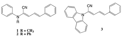
Designing organic materials for the fabrication of light emitting diodes (OLEDs) has been a research area of current interest since the ground-breaking work of Tang et al.1 and Friend et al.2 The OLED devices can be used for making low-cost display products. Continuing efforts have been spent not only on the development of new efficient materials, but also on ingenious device fabrications.3 In particular, the fabrication of multilayer structures and harvesting the light energy using dopants are attractive for high luminescent efficiency, high stability, and color tunability.4 A better understanding of the correlation between the energetics of charge carriers/interlayer barriers and the device performance will certainly aid the strategy for material choice and device configuration.In our previous study on the photochemistry of 2-(N-methylanilino)-5-phenylpenta-2,4-dienenitrile (1),5 it was found that some derivatives showed intense fluorescence upon photoexcitation. Molecular orbital calculations indicated that the highest occupied molecular orbital (HOMO) of 1 lies on the aniline–diene chromophore, whereas the lowest unoccupied molecular orbital (LUMO) lies along the cyano–diene part. In the excited state the molecule rotates along the N–C(diene) bond to form a twist intramolecular charge transfer state (TICT)6 with a high dipole moment (6.86 D). Adding electron-withdrawing groups on the aniline ring caused a blue shift of the emission, whereas adding the same groups on the phenyl ring on the other end caused a red shift.5 Such color-tuning properties may be valuable in designing electroluminescent materials in OLED applications. In this report, the electroluminescence properties of three related structures, i.e. compounds 1–3, are examined in order to explore their potential usage as light emitting materials in OLED devices.1
Experimental
Device fabrication
Prepatterned indium–tin oxide (ITO) substrates with an effective individual device area of 3.14 mm2 were cleaned by sonication in a detergent solution for 3 min and then washed with a large amount of doubly distilled water. Further sonication in ethanol for 3 min was done before the substrate was blown dry with a stream of nitrogen. The ITO substrates were then treated with oxygen plasma for 1 min before being loaded into the vacuum chamber. The organic layers were deposited thermally at a rate of 0.1–0.3 nm s−1 under a pressure of 2 × 10⁻⁵ Torr. Devices with a configuration of ITO/NPB/TBPI ∶ 2(or 3)/TBPI/Mg ∶ Ag, where NPB and TPBI are 4,4′-bis[N-(1-naphthyl)-N-phenylamino]biphenyl and 1,1′,1″-triphenyl-2,2′,2″-(benzene-1,3,5-triyl)tri-1H-benzimidazole respectively, were assembled with a thickness of 40, 20, and 20 nm for NPB, TPBI doped with 3% of 2 (or 3), and pure TPBI, respectively. Devices of the configuration ITO/NPB/CBP/TBPI ∶ 2(or 3)/TBPI/Mg ∶ Ag, where CBP is 4,4′-dicarbazolyl-1,1′-biphenyl, were assembled with 20, 20, 20, and 20 nm thickness of NPB, CBP, TPBI doped with 3% of 2 (or 3), and pure TPBI, respectively. A 50 nm cathode layer was deposited by co-evaporation of a Mg ∶ Ag alloy (ca. 10 ∶ 1 ratio). The device was completed by capping a Ag layer with 100 nm thickness (at rate 0.1–0.4 nm s−1).Instrumentation
1H and 13C spectra were obtained on a Bruker APX-400 spectrometer. Chemical shifts of 1H were measured downfield from TMS in δ units, while those of 13C were recorded with the central peak of CDCl3 at δ 77.00 as an internal reference. Mass spectra were obtained on a VG70-250S spectrometer or a VG Trio-2000 spectrometer. Infrared spectra were recorded on a Perkin-Elmer 682 infrared spectrophotometer. Absorption and emission spectra were recorded on a Hewlett-Packard 8453 absorption and a Hitachi F-4500 fluorescence spectrophotometer, and emission quantum yields were measured with reference to 9,10-diphenylanthracene. Elemental analyses were obtained on a Perkin-Elmer 2400 CHN instrument. Melting points were measured on a Thomas-Hoover mp apparatus and were uncorrected. Current–voltage–light intensity (I–V–L) of LEDs were measured using a Keithley 2400 source meter and a Newport 1835C multifunction optical meter, equipped with a silicon photodiode (Newport, model 818-ST). The measurements of I–V–L were performed simultaneously through an IEEE interface to a computer.2-Diphenylamino-5-phenylpenta-2,4-dienenitrile (2)
A round-bottomed flask fitted with a condenser was charged with diphenylamine (5.07 g, 30 mmol), aqueous formaldehyde solution (2.7 mL 37%, 33 mmol), and NaCN (1.47 g, 30 mmol) in acetic acid (20 mL). The solution was heated at 45 °C for 2 h, then was cooled and neutralized with dilute NaOH solution. It was extracted several times with ether. The combined ether layer was washed with saturated NaHCO3 and brine, dried over anhydrous MgSO4, and concentrated in vacuo. Diphenylaminoacetonitrile (2.50 g, 12 mmol) was collected by distillation at reduced pressure. Mp 50–53 °C; δH [CDCl3; 400 MHz] 4.51 (s, 2H), 7.03–7.12 (m, 6H), 7.31–7.37 (m, 4H); δC [CDCl3; 100 MHz; 1H-decoupled] 41.29, 106.00, 121.23, 123.51, 129.71, 146.37. Cinnamaldehyde (1.15 mL, 10.0 mmol) and diphenylaminoacetonitrile (2.08 g, 10.0 mmol) were dissolved in benzene (25 mL) containing K2CO3 (2.67 g) and KOH (0.56 g). The mixture was heated at 70 °C in a round-bottomed flask fitted with a condenser for 2 h. The reaction was quenched by the addition of water, and was extracted several times with ethyl acetate. The combined ethyl acetate solution was washed with brine, dried over anhydrous MgSO4, and concentrated in vacuo. Compound 2 (2.8 g, 9.0 mmol) was recrystallized from hexane as yellowish needles. Mp 147–149 °C (decomp.) (Found: C, 85.81; H, 5.72. C23H18N2 requires C, 85.68; H, 5.63%); νmax(KBr)/cm−1 3028, 2214, 1586, 1569, 1487, 1335; δH [CDCl3; 400 MHz] 6.55 (d, J = 17 Hz, 1H), 6.58 (d, J = 24 Hz, 1H), 7.11–7.16 (m, 6H), 7.18–7.25 (m, 2H), 7.25–7.38 (m, 6H), 7.42–7.46 (m, 2H); δC [CDCl3; 100 MHz; 1H-decoupled] 115.10, 119.28, 123.53, 124.32, 124.69, 126.81, 128.50, 128.79, 129.56, 132.22, 136.06, 136.40, 144.79; m/z (EI) 322 (80%), 321 (100), 245 (6), 219 (40).2-(Carbazol-9-yl)-5-phenylpenta-2,4-dienenitrile (3)
A round-bottomed flask fitted with a condenser was charged with carbazole (5.01 g, 30 mmol), bromoacetonitrile (2.75 mL, 36 mmol), K2CO3 (6.2 g), and KOH (1.68 g) in benzene (300 mL). The solution was heated to reflux for 18 h, then was cooled and neutralized with dilute HCl solution. It was extracted several times with ethyl acetate. The combined organic layer was washed with saturated NaHCO3 and brine, dried over anhydrous MgSO4, and concentrated in vacuo. Carbazol-9-ylacetonitrile (3.0 g, 15 mmol) was collected from a silica gel column chromatograph eluted with a mixture of hexane and ethyl acetate. Mp 137–138 °C (Found: C, 81.47; H, 5.07. C13H10N2 requires C, 81.53; H, 4.89%); νmax(KBr)/cm−1 3058, 2939, 1600, 1485, 1454, 1416, 1325; δH [CDCl3; 400 MHz] 7.33 (t, J = 7 Hz, 2H), 7.42 (d, J = 8 Hz, 2H), 7.53 (t, J = 7 Hz, 2H), 8.10 (d, J = 8 Hz, 2H); δC [CDCl3; 100 MHz; 1H-decoupled] 31.11, 108.26, 114.23, 120.76, 120.78, 123.74, 126.50, 139.44. Cinnamaldehyde (1.15 mL, 10.0 mmol) and carbazol-9-ylacetonitrile (1.03 g, 5.0 mmol) were dissolved in THF (15 mL) containing K2CO3 (1.04 g) and KOH (0.28 g). The mixture was heated at 70 °C in a round-bottomed flask fitted with a condenser for 2 h. The reaction was quenched by the addition of water, and was extracted several times with ethyl acetate. The combined ethyl acetate solution was washed with brine, dried over anhydrous MgSO4, and concentrated in vacuo. Compound 3 (0.8 g, 2.6 mmol) was collected as an orange solid. Mp 149–152 °C (decomp.) (Found: C, 85.94; H, 5.42. C23H16N2 requires C, 86.22; H, 5.03%); νmax(KBr)/cm−1 3025, 2925, 2209, 1620, 1598, 1480, 1449 cm−1; δH [CDCl3; 400 MHz] 7.37 (t, J = 8 Hz, 2H), 7.40–7.60 (m, 7H), 7.63 (d, J = 8 Hz, 2H), 7.71–7.80 (m, 3H), 8.21 (d, J = 8 Hz, 2H); δC [CDCl3; 100 MHz; 1H-decoupled] 108.11, 111.07, 114.82, 121.43, 122.21, 122.77, 124.79, 127.54, 128.67, 130.00, 130.81, 136.69, 140.79, 144.10, 145.62; m/z (EI) 320 (100%), 291 (10), 242 (20), 229 (20), 163 (30), 202 (8).Results and discussion
The absorption and emission spectra
The synthesis of compound 1 has been described previously, and a similar procedure was followed in preparing 2 and 3.5 They are yellowish solids with green fluorescence, and their absorption and emission spectra in cyclohexane are shown in Fig. 1. There are two major absorption bands in the range of 280–420 nm, one at λmax 360–390 nm and another at 300–320 nm. The λmax values of the low energy bands of 2 and 3 are red-shifted with respect to that of 1, as a result of extended delocalization of the nitrogen lone pair onto the additional phenyl rings. The trend is consistent with semiempirical estimations shown in Fig. 2. Irradiation of 1 at 360 nm gave rise to a broad emission at λmax 480 nm (Φf = 0.07), while irradiation of 2 and 3 at 390 nm yielded emissions at λmax 475 (Φf = 0.47) and 435 nm (Φf = 0.39), respectively. Fluorescence quantum yields (Φf) were measured in cyclohexane using 9,10-diphenylanthracene as a standard.7 The emission intensities of 2 and 3 are much stronger than that of 1.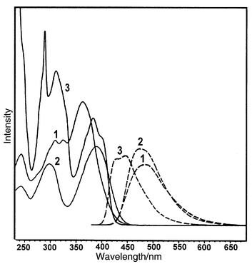 | ||
| Fig. 1 The absorption (solid lines) and emission (dashed lines) spectra of compounds 1–3 in cyclohexane. Their relative intensities are not normalized. | ||
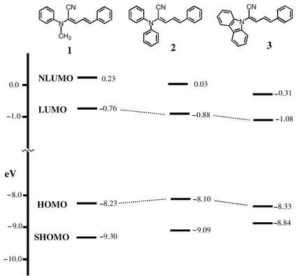 | ||
| Fig. 2 The calculated energy levels of compounds 1, 2 and 3, where the geometry of the molecules is fully optimized by AM1.8 | ||
The emission spectrum of 3 showed a smaller Stokes shift than those of 1 and 2, since the degree of conformational change of the former during excitation is expected to be less than those of the latter. The carbazole nitrogen in 3 is locked coplanar with the rings, yet the N-phenyl moieties of 1 and 2 cannot be totally coplanar with the diene due to the steric hindrance. The calculated frontier orbitals of 1–3 by AM1,8 with full geometrical optimization, are shown in Fig. 2. The results simulate their electronic configuration in the ground state in the gas phase. In methylene chloride, the oxidation potentials of 1, 2, and 3 were measured by cyclic voltametry to be 1.06, 1.09 and 1.12 V, respectively. Since the oxidation waves are not completely reversible, structural changes occurred during the electrochemical processes. These oxidation potentials can be correlated to the HOMO and LUMO levels by the equation IP = Eox + 4.40 eV,9 and were estimated to be 5.46 and 2.45 eV for 1, 5.49 and 2.67 eV for 2, and 5.52 and 2.56 eV for 3. The HOMO and LUMO values are useful in understanding/designing the device characteristics/configuration.
Fabrication of LED devices
Electroluminescent devices were attempted with compounds 1, 2, and 3 as emitting dyes. Two types of devices were fabricated. In one the dye was doped into the electron-transporting material (ETL) of a single hetero-junction device using NPB as the hole-transporting layer (HTL) and TPBI as the ETL. TPBI was chosen as the ETL since it is a well-known electron transporting material10 and a significant spectral overlap is found between the emission spectrum of TPBI and the absorption spectra of the dyes examined, which fulfills the requirement of a Forster type energy transfer. In the other type of device, the dye was doped into a polymer layer polycarbazolylethylene (PVK) by spin-coating. The molecular structures of several film-forming materials used in the study are as shown.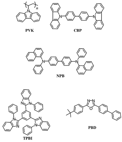
Using TPBI as the host
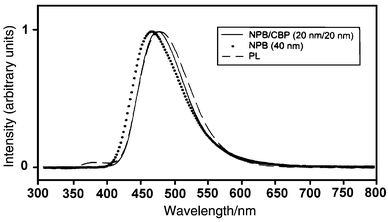
A device of structure ITO/NPB/TPBI ∶ 2(or 3)/TPBI/Mg ∶ Ag was constructed. A 40 nm of NPB film was deposited on ITO glass followed by 20 nm of TPBI doped with 3% by weight of the dye. Another 20 nm layer of pure TPBI was deposited to isolate the doped layer from the electrode contact. The performances of the devices are presented in Fig. 3–6. The devices for both 2 and 3 gave a turn-on voltage around 6 V and a luminance of ∼6000 Cd m−2 for a 2-doped and ∼2000 Cd m−2 for a 3-doped device at a drive voltage of 15 V. External quantum efficiencies of 0.75% and 0.25% were achieved for 2- and 3-doped devices respectively. The EL spectrum, shown in Fig. 8, indicates some blue shift of the emission from the photoluminescence spectrum of the same doped film. It was reported that the TPBI may serve as a hole-blocker when used in conjunction with NPB in a two-layer device configuration.11–13 A CBP layer inserted between the NPB and TPBI layers could effectively promote the transporting of holes into the TPBI layer because of the reduction of the barrier to crossing by introduction of an intermediate level (HOMO of CBP 5.5 eV) between the HOMO of NPB (5.2 eV) and that of TPBI (6.2 eV) (Fig. 7). Thus a device configuration of ITO/NPB/CBP/TPBI ∶ 2(or 3)/TPBI/Mg ∶ Ag was constructed. While the I–V characteristics showed that a lower current was obtained at the same voltage under this configuration than in the absence of a CBP layer, the luminance as well as external quantum efficiency were much improved. A maximum luminance of >9000 Cd m−2 for 2- and ∼5000 Cd m−2 for 3-doped device was obtained respectively. The external quantum efficiency was also enhanced, with 1.7% for 2 and 0.9% for 3-doped devices (Fig. 3–6). While these devices are not yet optimized, their performances are already comparable with those typical blue- and green-light emitting devices of similar fabrications.12–14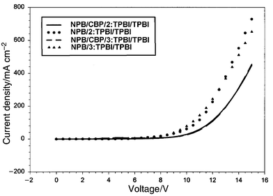 | ||
| Fig. 3 The I–V plots for the devices made with 2 and 3. The compositions are shown in the inset. | ||
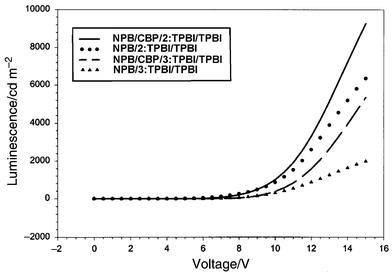 | ||
| Fig. 4 The L–V plots for the devices made with 2 and 3. The luminescence intensity was higher in the presence of CBP in both cases. | ||
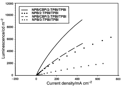 | ||
| Fig. 5 The L–I plots for the devices made with 2 and 3 fabricated with and without CBP. | ||
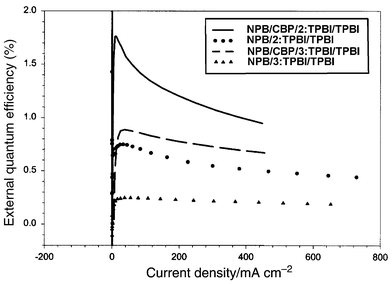 | ||
| Fig. 6 External quantum efficiencies for the devices made with 2 and 3. A better performance was clearly shown in the presence of a CBP layer. | ||
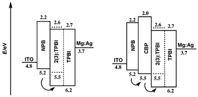 | ||
| Fig. 7 Relative HOMO/LUMO energy levels in the single (left) and double (right) hetero-junction designs. In the absence of CBP, the transportation of holes from NPB to TPBI was slow due to a higher energy barrier (ca. 1.0 eV). In the presence of CBP, the flow of holes was faster with reduction of the barriers (right). | ||
 | ||
| Fig. 8 Emission spectra of 3 in three different forms, i.e. the photoluminescence of a thin film (dashed line), the electroluminescences of LED devices without CBP (dotted line) and with CBP (solid line). The weak band at λmax 375 nm is derived from TPBI. | ||
Fig 8 shows the emission spectra obtained for the devices, where the influence of CBP can be further seen. The photoluminescence of 3 doped in TPBI (at 3%) is shown by a dashed line as a standard. The weak band at λ 375 nm is a residual emission of TPBI, as a result of incomplete energy transfer. In the presence of CBP, the EL spectrum overlaps nicely with the PL spectrum. The small shoulder at 375 nm vanished, probably because an alternative emission mechanism operates in addition to the Forster energy transfer mechanism. In contrast, the EL in the absence of CBP layer showed a slight “blue shift” (dotted line in Fig. 8) compared to the PL. The “blue shift” became more apparent at higher applied voltages, e.g. 14 V vs. 8 V, when more electrons were pushed into the NPB layer. A very similar behavior was observed in the case of the 2-doped device.
Using PVK as host
Compound 1 was known to undergo photodimerization upon UV irradiation, therefore it was blended into PVK polymer to reduce molecular aggregation.5 The PVK polymer served both as a hole transporting material and as an energy donor. A concentration analysis on the fluorescence of 1 indicated that energy transfer from PVK to 1 occurred effectively in solutions with concentrations higher than 3% by weight. The carbazole emission at 410 nm was quenched completely upon irradiation at 340 nm, while only the emission of 1 at 480 nm was observed.Three different weight ratios (1%, 3%, and 5%) of the blended material in CH2Cl2 were spin-coated onto the surface of ITO glass to form films of ca. 100 nm thick. It was covered with a thin layer of TPBI (as the ETL) by vapor deposition. The two organic layers were covered by a layer of Mg–Ag (10 ∶ 1) alloy, followed by a pure silver layer as the anode. L–V plots showed that the device began to emit green light at 13 V at blending ratios of 3% and 5% (Fig. 9). A closer look at the emission spectra showed that at 1% weight ratio the light was emitted entirely from the carbazole moieties of PVK (λmax at 400 nm), while at higher concentrations the emission of 1 at λmax 500 nm began to increase. It was clear that the energy transfer from carbazole to 1 was not satisfactory even at 5% weight ratio. The luminance is, nevertheless, rather low.
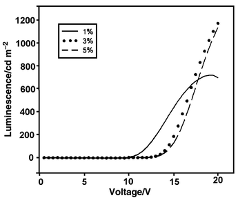 | ||
| Fig. 9 Intensity versus voltage plots for LED devices fabricated by blending compound 1 into PVK at three different weight percentages. At 1% doping ratio, the emission derived totally from PVK. | ||
In an attempt to increase the current density and the efficiency of energy transfer, the weight ratio of 1 was increased to 10% and NPB was added into the blends. In a similar process, a device was fabricated using a mixture of compound 1, NPB, and PVK in a weight ratio 10 ∶ 40 ∶ 100. The device started emitting at 12 V, and the brightness reached 100 Cd m−2 at 20 V. The spectra matched that of 1, indicating a complete energy transfer from PVK to 1. However, the external quantum efficiency was still too low (0.015%) to be of any practical value.
2-(Biphenyl-4-yl)-5-(4-tert-butylphenyl)-1,3,4-oxadiazole (PBD) has been widely used as an efficient electron transporting material and it was chosen to be another additive to the blend. A mixture of compound 1 ∶ NPB ∶ PBD ∶ PVK in weight ratios 3 ∶ 50 ∶ 50 ∶ 100 was used to assemble a single layer device. The material was spin-coated on ITO, followed by the deposition of Mg ∶ Ag electrode as described before. The device began to emit green light at about 12 V. The emission spectrum with λmax at 500 nm was slightly red-shifted compared with the PL of 1. A maximum luminescence of 650 Cd m−2 and a current density of 460 mA cm−2 were obtained at 23 V (Fig. 10). The optimal external quantum efficiency was much better than the one without PBD (ca. 0.10 %). Nevertheless, the performance of this device was much poorer than the double hetero-junction devices fabricated for 2 and 3 earlier, presumably due to the intrinsic nature of the compounds itself (low Φf) as well as the method of fabrication for the devices (multi-layer by vapor deposition vs. single-layer by spin-coating).
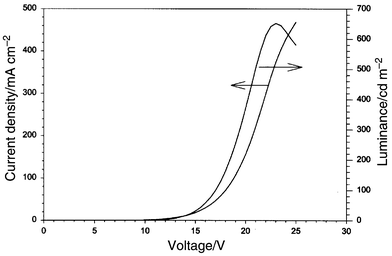 | ||
| Fig. 10 I–V–L plots for a single layer LED device using a blend of compounds containing 1 ∶ NPB ∶ PBD ∶ PVK in weight ratio 3 ∶ 50 ∶ 50 ∶ 100. | ||
Conclusion
It was demonstrated that the derivatives of 2-anilino-5-phenylpenta-2,4-dienenitrile (1–3) may be used as electroluminescent materials in organic LED fabrications. Better performance was achieved with a device configuration of ITO/NPB/CBP/TPBI ∶ 2(or 3)/TPBI/Mg ∶ Ag, where two layers of hole-transporting materials NPB/CBP was used. A turn-on voltage of ∼6 V for both 2- and 3-doped devices and a maximum luminance of >9000 Cd m−2 and ∼5000 Cd m−2, respectively, were observed. The optimal external quantum efficiencies were found to be 1.7% for 2- and 0.9% for 3-doped devices.Single layer devices of 1 blended in PVK along with other charge transporting materials were fabricated by spin-coating method. The performance was not quite as good as those of 2 and 3; however, these devices have not yet been fully optimized and there is scope for further improvements.
All the results reported in this paper have been reproduced in repeat tests on separately fabricated devices. However, cells with optimized sealing to prevent atmospheric oxidation have not yet been fabricated. This group of compounds is also known to undergo photochemical reactions upon irradiation.5 Work is currently in progress to characterize and optimize the thermal, photochemical and electrochemical stability of these devices, both by improved fabrication methods and by structural modification of the compounds, which is also aimed at further improving the efficiency and colour-tuning.
Acknowledgements
Financial supports from Academia Sinica and the National Science Council of Republic of China are gratefully acknowledged. Some helpful comments by the editors of this journal through the reviewing processes are also appreciated.References
- C. W. Tang and S. A. VanSlyke, Appl. Phys. Lett., 1987, 51, 913 CrossRef CAS.
- J. H. Burroughes, D. D. C. Bradley, A. R. Brown, R. N. Marks, K. Mackay, R. H. Friend, P. L. Burns and A. B. Holmes, Nature, 1990, 347, 539 CrossRef CAS.
- (a) J. Shi and C. W. Tang, Appl. Phys. Lett., 1997, 70, 1665 CrossRef CAS; (b) C. W. Tang, S. A. Van Slyke and C. H. Chen, J. Appl. Phys., 1989, 65, 3610 CrossRef CAS; (c) F. Steuber, J. Staudigel, M. Stossel, J. Simmerer, A. Winnacker, H. Speritzer, F. Weissortel and J. Salbeck, Adv. Mater., 1999, 12, 130 CrossRef CAS; (d) M. A. Baldo, D. F. Obrien, Y. You, A. Shoustikov, S. Sibley, M. E. Thompson and S. R. Forrest, Nature, 1998, 395, 104; (e) C. Adachi, S. Tokito, T. Tsutsui and S. Saito, Jpn. J. Appl. Phys., Part 2, 1988, 27, 269 Search PubMed; (f) M. Uchida, C. Adachi, T. Koyama and Y. Taniguchi, J. Appl. Phys., 1999, 86, 1680 CrossRef CAS.
- (a) Organic Electroluminescent Materials and Devices, eds. S. Miyata and H. S. Nalwa, Gordon and Breach, Amsterdam, 1997 Search PubMed; (b) Acc. Chem. Res. 1999, 32, 191, a special issue on molecular materials in electronics and optoelectronic devices Search PubMed; (c) H. Ishii, K. Sugiyama, E. Ito and K. Seki, Adv. Mater., 1999, 11, 605 CrossRef CAS.
- Y.-L. Liang, J.-M. Fang, T. Chow, T.-I. Ho, C.-R. Lee and Y. Wang, J. Org. Chem., 1994, 59, 5742 CrossRef CAS.
- W. Rettig, Angew. Chem., Int. Ed. Engl., 1986, 25, 971 CrossRef.
- J. V. Morris, M. A. Mahaney and J. R. Huber, J. Phys. Chem., 1976, 80, 969 CrossRef CAS.
- M. J. S. Dewar, E. G. Zoebisch, E. F. Healy and J. J. P. Stewart, J. Am. Chem. Soc., 1985, 107, 3902 CrossRef.
- S. Janietz, D. D. C. Bradley, M. Grell, C. Giebeler, M. Indasekaran and E. P. Woo, Appl. Phys. Lett., 1998, 73, 2453 CrossRef CAS.
- Z. Q. Gao, C. S. Lee, I. Bello, S. T. Lee, S. K. Wu, Z. L. Yan and X. H. Zhang, Synth. Met., 1999, 105, 141 CrossRef CAS.
- B. E. Koene, D. E. Loy and M. E. Thompson, Chem. Mater., 1998, 10, 2235 CrossRef CAS.
- Y.-T. Tao, E. Balasubramaniam, A. Danel and P. Tomasik, App. Phys. Lett., 2000, 77, 933 Search PubMed.
- E. Balasubramaniam, Y.-T. Tao, A. Danel and P. Tomasik, Chem. Mater., 2000, 12, 2788 CrossRef.
- (a) J. Kido and Y. Lizumi, Chem. Lett., 1997, 963 CrossRef CAS; (b) C. Hosokawa, H. Higasi, H. Nakamura and Y. Kusumoto, Appl. Phys. Lett., 1995, 67, 3853 CrossRef CAS; (c) Z. Q. Gao, C. S. Lee, I. Bello, S. T. Lee, R. M. Chen, T. Y. Lu, J. Shi and C. W. Tang, Appl. Phys. Lett., 1999, 74, 865 CrossRef CAS; (d) Y. T. Tao, E. Balasubramaniam, A. Danel, A. Wisla and P. Tomasik, J. Mater. Chem., 2001, 11, 768 RSC; (e) K. R. J. Thomas, J. T. Lin, Y.-T. Tao and C.-W. Ko, Adv. Mater., 2000, 12, 1949 CrossRef CAS.
| This journal is © The Royal Society of Chemistry 2002 |