Quantitative 3-dimensional profiling of channel networks within transparent ‘lab-on-a-chip’ microreactors using a digital imaging method
Ian
Broadwell
,
Paul D. I.
Fletcher
*,
Stephen J.
Haswell
,
T.
McCreedy
and
Xunli
Zhang
Department of Chemistry, The University of Hull, Hull, UK HU6 7RX. E-mail: P.D.Fletcher@chem.hull.ac.uk
First published on 9th August 2001
Abstract
We have developed a method for the quantitative 3-dimensional profiling of micron sized channel networks within optically transparent “lab-on-a-chip” microreactor devices. The method involves capturing digitised microscope images of the channel network filled with an optically absorbing dye. The microscope is operated in transmission mode using light filtered through a narrow bandpass filter with a maximum transmission wavelength matching the wavelength of the absorbance maximum of the dye solution. Digitised images of a chip filled with solvent and dye solution are analysed pixel by pixel to yield a spatially resolved array of absorbance values. This array is then converted to optical path length values using the Beer–Lambert law, thereby providing the 3D profile of the channel network. The method is capable of measuring channel depths from 10 to 500 µm (and probably even smaller depths) with an accuracy of a few percent. Lateral spatial resolution of less than 1 µm is achievable. It has been established that distortion of the measured profiles resulting from a mismatch in refractive index between the dye solution and the glass of the microreactors is insignificant. The method has been successfully used here to investigate the effects of thermal bonding and etch time on channel profiles. The technique provides a convenient, accurate and non-destructive method required to determine channel profiles; information which is essential to enable optimisation of the operating characteristics of microreactor devices for particular applications.
Introduction
There is increasing interest in the development of miniaturised microreactor devices for a wide range of analytical, chemical synthesis and other measurements as encompassed in the so-called ‘lab-on-a-chip’ concept. The microreactor designs developed and used by the Hull group consist of a network of micron-sized channels connecting a number of reagent reservoirs which also hold the electrodes used for electro kinetic pumping. Timed voltage sequences applied under computer control to the appropriate pairs of reservoir electrodes may be used to control the movement (and hence the chemical reactions) of reagents within particular regions of the channel network by a combination of electro-osmotic and electrophoretic effects. This enables control of the spatial and temporal evolution of chemical reactions in microreactors in a manner not achievable in conventional batch reactors. It has been demonstrated that this control can be used to alter the yields and selectivities of product mixtures for a range of different reactions performed in microreactors (see refs. 1–6 for recent progress in this area). The theoretical principles of electrokinetic control of chemical reactions in microreactors have been reviewed previously.7The particular microreactor designs used in Hull (and by other researchers) are fabricated by etching a channel network into a glass base plate of typical dimensions 20 mm wide × 20 mm deep × 2 mm thick.5,8,9 The etched base plate is then thermally bonded to a thick glass upper plate (thickness typically 15 mm) containing pre-drilled holes of about 3 mm diameter which connect to the channel network and act as reagent reservoirs. In order to quantitatively predict and control the electrokinetic movement of reagents within the microreactors it is necessary to determine the full 3D profiles of the channel networks in the assembled microreactor devices. In addition, control and optimisation of the base etching and thermal bonding processes also require methods for 3D profiling of both non-bonded and bonded base plates. A key consideration here is the possible extent to which the thermal bonding of the upper and base plates may distort the channel profile. For the open etched base plates before bonding, 3D profiles can be obtained using mechanical, stylus-based techniques. For such methods, care must be taken to avoid artefacts at the near vertical channel edges arising from the limited resolution and imperfections in the shape of the stylus tip. For the closed, bonded base plates, it is possible to obtain the channel profile by cutting the bonded device perpendicular to the channel axis followed by microscopically imaging the channel profile. This procedure has a number of disadvantages. Firstly, the device is destroyed by the measurement. Secondly, the channel profile is only obtained at a single point where the cut is made. Lastly, it is not a trivial matter to obtain the channel cross section accurately without artefacts due to ‘chipping’ of the edges arising from the cutting process. In order to meet the need for a rapid, accurate and non-destructive method for 3D profiling of both open and closed etched channel networks, we have developed a technique based on digital microscopic imaging of the channel network filled with an optically absorbing dye solution (see Fig. 1). The method is generally applicable for the quantitative 3-dimensional profiling of any voids fillable with dye solution which are present in a transparent solid. In this paper we describe the application of the method for the profiling of channel networks within a range of bonded and non-bonded microreactor devices.
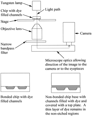 | ||
| Fig. 1 Schematic diagram of the inverted optical microscope arrangement used for the 3D profiling of microreactor chip channel networks. The lower diagrams show side views of dye filled channels (shaded gray) in a bonded chip and in a non-bonded chip covered with a non-bonded top plate. | ||
The method described here is similar in principle to a range of (generally more complex) spectroscopic imaging techniques (UV/vis, IR, Raman) which have been developed for particular applications.10–16 The absorbance imaging method described here is simple to implement and provides absolute values of the channel depths.
Experimental
1 Materials
m-Cresol (Lancaster, 99%), glycerol (Lancaster, >99%), Patent Blue (Fluka standard reagent), Rose Bengal (Aldrich, dye content approx. 95%) were used without further purification. Water was purified by reverse osmosis.2 Methods
An Axiovert S100 inverted microscope (Carl Zeiss) using transmission optics was employed to obtain digital micrographic images of the microreactors filled with either solvent or dye solutions. The light source was a 100 W tungsten lamp emitting over the wavelength range from approximately 400 to 800 nm. Wavelength selection appropriate to the particular dye solution used was achieved by incorporating an appropriate narrow band pass filter of the correct maximum transmission wavelength between the microscope objective and camera (Fig. 1). Transmittance spectra of the two filters used here (Chroma 11002, peak 546 nm full width at half maximum 10 nm and Edmund Scientific N43-136, peak 649, full width at half maximum 11 nm) are given in Fig. 2. Stray ambient light was reduced to negligible levels by use of a hood over the microscope. Microscope images were collected using a digital monochrome CCD camera (Hamamatsu C4742-95-12NRB) giving a digital output of a maximum of 1024 × 1024 pixels with 12 bit resolution of the light intensity in each pixel. The camera was connected to a PC and controlled by the digital image recording and analysis software AQM from Kinetic Imaging Ltd. Averaging of pixel intensities over 4 × 4 groups of pixels (‘4 × 4 binning’) was used to yield a 256 × 256 array of intensity values. This procedure was found to provide the best compromise between rapid data acquisition, signal-to-noise ratio, spatial resolution and data file size. Scion Image software (Scion Corporation) was used to transfer the numerical image data into Microsoft EXCEL for subsequent conversion into absorbance values and hence pixel-by-pixel depth values.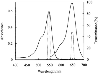 | ||
| Fig. 2 Absorbance spectra of RB (1.0567 mM in water, λmax = 547 nm) and PB solutions (0.8275 mM in 30.2 wt.% glycerol in m-cresol, λmax = 647 nm). The path length was 100 µm. The dashed lines show the transmittance curves for the two narrow bandpass filters used in conjunction with the different dye solutions. | ||
As explained in detail below, for the profiling measurements by the imaging technique it is necessary to capture images of the microreactor filled with dye solution and filled with solvent. For the proper calculation of pixel-by-pixel absorbance values, it is essential that there is no movement of the microreactor between the capture of these two images. Hence, care was taken to ensure that the microreactor was firmly located in a fixed position on the microscope stage and filled with the appropriate liquid in situ using syringes. For 3D profiling of non-bonded base plates, the etched channels were filled with either solvent or dye solution and then covered with a non-bonded top plate. This procedure always gave a thin layer of dye in the non-etched regions of the base plate (see detail in Fig. 1). This small measured thickness of dye solution was subtracted from the derived values to obtain the true channel depths. Dye solution UV/Vis spectra and absorbance values required for calibration were recorded using a Unicam UV3 spectrophotometer using quartz cuvettes (Hellma) with accurate path lengths in the range 50–10000 µm.
Microreactor devices were fabricated according to published procedures.9 The base plate of chip 1 was etched using a solution comprising 250 ml of water, 12.5 g ammonium fluoride (Lancaster, 98%) and 7 ml of 40% HF solution in water (BDH Merck, AnalaR grade) for 25 min at 65 °C. The base was placed on a support in the etch solution with patterned side facing downwards within a heated ultrasonic bath (Ultrawave Scientific Supplies, Nottingham, UK). Ultrasound was applied in 1 min bursts at 5 min intervals. This procedure has been found to ensure that debris is effectively removed during the etch and that fresh etchant solution remains in good contact with the surface. Thermal bonding of chip 1 was made as follows. The base and upper plates were placed on a flat quartz plate in a conventional muffle furnace and a block of quartz of mass 70 g was placed on top to aid bonding. The oven temperature was then held at 575 °C for 3 h. Chip base 2 was etched similarly except that the etching temperature was 60 °C and the solution was stirred with a rod instead of using ultrasound. It was thermally bonded using an oven temperature of 570 °C for 3 h using a quartz top block of mass of 28 g. Chip bases 3–7 (non-bonded) were etched for variable times using an etch bath temperature of 60 °C with ultrasonication (non-continuous, 1 min on followed by 9 min off) to aid debris removal.
Results and discussion
1 Imaging procedure to obtain 3D profiles
The optical absorbance A of a solution is given by the Beer–Lambert law.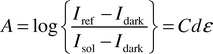 | (1) |
To obtain d, the following sequence of images was captured for each sample using the apparatus shown schematically in Fig. 1.
1. Image of the channels with zero incident illumination to obtain the array of Idark intensities.
2. Image of the channels filled with solvent giving the array of Iref intensities.
3. Image of the channels filled with dye solution giving the array of Isol intensities.
For each measurement set, the incident light intensity and the camera gain were adjusted so that the maximum intensities in the Iref array were close to the maximum value of 4095 allowed by the 12 bit resolution of the camera. It was monitored that, under the set conditions, the array of Idark values did not exceed 200 or so. This procedure ensured that the full dynamic range allowed by the 12 bit resolution of the camera was used.
Solutions of two different dyes were used in this study. The spectra of RB (Rose Bengal) and PB (Patent Blue) solutions are shown in Fig. 2 and compared with the transmittance curves of the narrow band pass optical filters used in the microscope imaging. The water-soluble dye RB was used in aqueous solution for which the refractive index (RI) of approximately 1.33 is not matched to that of the glass (approximately 1.5). Because of this lack of RI matching, optical refraction is expected at the channel edges which may give some distortion of the measured channel profile. The profiling of non-bonded base plates requires that the dye solution be spread on the etched channel surface of the base before covering with a non-bonded top plate. In early experiments with RB and other dye solutions, problems were encountered due to significant evaporation of the dye solution during this procedure, resulting in uncontrolled changes in dye concentration. We developed the PB dye solution with the following characteristics required to optimise the 3D profiling method. The dye solution should be matched in RI with the glass of the microreactor chip and must be involatile. The dye must be highly soluble in the solvent in order that sufficiently high absorbance required to profile channels of low depth (i.e. small path lengths). It is advantageous if the absorbances of the dye solutions are proportional to concentration. This facilitates the optimisation of dye concentration necessary to minimise experimental uncertainties for different channel depths. The dye solutions should be chemically stable and the absorbance of the solvent should be negligible compared to that of the dye solution at the optimum wavelength.
These characteristics were fulfilled by PB solutions in a mixed solvent consisting of 30.2 wt.% glycerol in m-cresol. Fig. 2 shows the spectrum of a PB solution. Fig. 3 shows plots of absorbance at 647 nm versus PB concentration for different path lengths recorded using a conventional spectrophotometer. It is clear that sufficiently high absorbance values can be obtained and that the Beer–Lambert law is obeyed with reasonable precision. For the PB solutions, full dissolution of the dye required treatment in an ultrasonic bath for several hours. Absorbance measurements over several weeks showed the dye solutions have adequate stability for reliable imaging measurements.
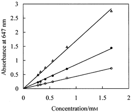 | ||
| Fig. 3 Absorbance (647 nm, measured using a conventional spectrophotometer) versus PB concentration in glycerol–cresol mixed solvent for path lengths of 50 (open circles), 100 (filled circles) and 200 µm (open triangles). | ||
The accuracy with which d can be determined for each image array value (corresponding to a single ‘binned’ pixel group) depends on the value of the absorbance. For the setup used here, the typical experimental uncertainty in each of the intensity values Iref, Isol and Idark was estimated from the variation in measured arrays of intensity values to be approximately ±5. The values for Idark and Iref using optimised settings for the incident light intensity and camera gain were typically 100 and 3500 respectively. Conversion of the uncertainties in the individual (binned) pixel intensities to the uncertainties in derived absorbance yields the plot shown in Fig. 4. The uncertainty in absorbance, and hence in depth d, is minimum for absorbance values of around 0.6 and is approximately 2%. Since absorbance is proportional to channel depth, the dye concentration used must be adjusted in order to achieve the optimum absorbance of 0.6 for the particular channel depth under study and an acceptable uncertainty of 2% in d.
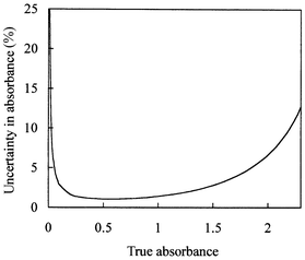 | ||
| Fig. 4 Variation of percentage uncertainty in the measured absorbance with true absorbance for Idark = 100 and Iref = 3500. Uncertainties of ±5 in each of the intensities Idark, Iref and Isol were assumed. | ||
An additional possible source of systematic error in the measurement of d arises from the fact that microscope objectives have a significant numerical aperture NA, meaning that light rays passing through the sample take on a variety of paths with different angles. A microscope objective lens accepts light over a cone in the angle range ±α relative to the perpendicular. For an air objective, NA = sinα. Hence the actual path length experienced by a light will be the intensity weighted average for all angles between 0 and α. The maximum error in the channel depth measurement can be estimated by calculation of the ratio xmax = (true perpendicular path length/max light path length). The maximum light path length occurs for light rays at the maximum acceptance angle α and is equal to cos(sin−1NA). The effective path length measured will differ from the perpendicular value by the intensity distribution weighted average <x> which will be intermediate between 1 and xmax. As an approximate estimate of this effect, we take <x> to be (1 + xmax)/2. For the objective lenses used in this work with magnifications of 1.25, 2.5, 4 and 10×, the values of NA are 0.035, 0.075, 0.1 and 0.3 respectively. The corresponding values of <x> are 0.9997, 0.9986, 0.9975 and 0.9770. Thus, it can be seen that the errors in channel depth introduced by this effect are negligible so long as objectives of 10× or less are used. Proper correction for the effect would be required when using objectives of higher magnification.
It was checked that the microscopic imaging method yielded reliable absorbance measurements. Images of dye filled rectangular capillaries of different path lengths (obtained from Camlab, UK) and a 1 mm cuvette were recorded and converted to absorbance. The absorbance of the 1 mm cuvette sample was also measured using a conventional spectrophotometer. The results, plotted in Fig. 5, show that the microscope absorbance values agree within the experimental uncertainties (mainly arising from the uncertainties (±7%, estimated microscopically) in the path lengths of the capillaries).
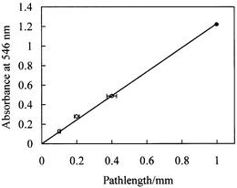 | ||
| Fig. 5 Absorbance (546 nm, measured using the microscope imaging method) versus path length for dye filled capillaries or rectangular cross section (open circles) and a 1 mm path length cuvette (filled circle). | ||
Fig. 6 shows a 3D profile image of a 7 × 7 mm area of chip 1 recorded using a 1.5× objective lens. Even at this low magnification (required to image a large area) the spatial resolution is sufficient to allow details of the channel profiles and intersections to be seen clearly. The deep circular shape at X = 7800, Y = 0 mm corresponds to one of the reservoirs on the microreactor. When viewed on the computer screen using EXCEL software, the image can be fully rotated in 3D allowing examination from all angles. The time required for acquisition of the image set and subsequent data analysis to produce Fig. 6 was about 1 h.
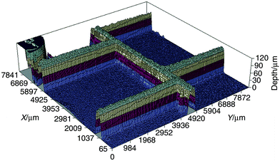 | ||
| Fig. 6 3D profile image of a 7 × 7 mm area of the channel network of chip 1. The image was recorded using RB as the dye (non-RI matched). | ||
Higher magnification images using a 10× objective of a sub-area of chip 1 were recorded using both aqueous RB (non-RI matched) and glycerol–cresol PB dye (RI matched) solutions. The aim here was to determine whether non-RI matching between the dye solution and the glass of the microreactor produces significant distortion of the channel profiles due to refraction of the light at the channel edges. 2D ‘slices’ through the channels at corresponding positions in the two full 3D profiles are shown in Fig. 7. It can be seen that non-RI matching does not produce any significant distortion of the channel profiles. This conclusion is valid for aqueous RB solutions with an RI of approximately 1.33 as compared with approximately 1.52 for the glass. Although a higher level of mismatch in RI may produce significant distortion, it is important for many future microreactor applications to establish that use of aqueous solutions in glass microreactors in the context of imaging methods does not give significant distortion.
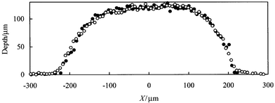 | ||
| Fig. 7 Comparison of channel cross sectional profiles for chip 1 obtained using RB aqueous dye solution not RI matched to the glass (filled circles) and PB solution in glycerol–cresol mixed solvent which was RI matched to the glass (open circles). The two channel cross sections correspond to the same position in the channel network of chip 1. | ||
Fig. 8 shows an optical micrograph of one end of a channel which was etched right up to the edge of chip 1. This was done to enable us to compare the channel profile without the necessity for cutting the chip open. The dimensions of the channel end profile imaged in Fig. 8 shows reasonable agreement with those determined from the imaging measurements of Fig. 7.
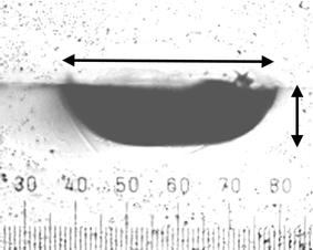 | ||
| Fig. 8 Micrograph of a side view of a channel end in chip 1. The horizontal arrow length (409 µm) corresponds to the channel top width measured in Fig. 7. The vertical arrow length (119 µm) corresponds to the channel depth measured in Fig. 7. | ||
2 Comparison of channel profiles before and after thermal bonding of the upper plate
Figs. 9a and 9b show 3D profile images recorded before and after thermal bonding of chip 2. The channel cross sections at corresponding positions in the two 3D images are compared in Fig. 10 where it can be seen that the effect of bonding has been to “squash” the channels from an initial depth of 55.3 down to 39.9 µm.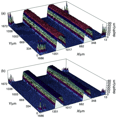 | ||
| Fig. 9 Comparison of 3D profile images of a 1.7 × 1.7 mm area of chip 2 (a) before and (b) after thermal bonding of the base and upper plates. The images were recorded using PB as the dye (RI matched). | ||
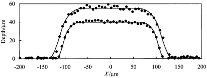 | ||
| Fig. 10 Channel cross sectional profiles for chip 2 before (larger depth) and after thermal bonding (smaller depth) of the base and upper plates. The co-ordinates of the channel centres correspond to X = 500 and Y = 615 µm in Fig. 9. The solid curves are best-fits to the model described in the text with the parameters listed in Table 1. | ||
The etching of glass, using the etch solution described above, proceeds at equal rates in all directions, i.e. the etching is isotropic. The etch depth d is controlled by the etch conditions and the etch time. Ideal isotropic etching through a channel mask of width m is expected to produce a channel profile comprising a rectangular shape of width m and depth d bounded by two quarter circle edges of radius equal to d. The expected channel width at the glass surface is equal to (m + 2d). In practice, either prolonged etching or thermal bonding may produce a ‘smoothing’ of the channel edges away from the idealised quarter circle shape. In order to model the channel profiles, we first calculate the ideal isotropic etch profile using the values of m and d. The ‘smoothing’ of the profile is then parameterised by incorporation into the model of a variable smoothing length δ. The channel depth at each X value is obtained by taking the depth calculated for the isotropic etch profile averaged over the range of X values corresponding to ±δ. Fitting of the experimental channel profiles then yields the best-fit values of m, d and smoothing length δ. A zero value of δ corresponds to no distortion from the idealised isotropic etch profile whereas a high value indicates that significant smoothing has occurred during either the etching or thermal bonding processes.
For the profiles of Fig. 10, the solid lines shows the best fits to the smoothed isotropic etch model. The derived parameters for chip 2 (shown in Table 1) show relatively low values of δ indicating little distortion from the isotropic etch profile. Thermal bonding in this case apparently reducesδ slightly. However, it can be seen in Fig. 10, that the difference in channel profile shapes corresponding to the best fit values of δ of 25 and 15 µm (for the non-bonded and bonded chips respectively) is rather small. In contrast to chip 2, the δ values for chip 1 (Table 1, where similar values are seen for non-RI and RI matching) are high indicating that significant smoothing of the channels occurred during the fabrication of this chip. It is relevant to note here that chip 1 was bonded using a higher temperature and a larger top mass (added to aid bonding) than chip 2. Both factors might be expected to increase channel profile distortion during bonding. These examples serve to demonstrate the utility of the 3D profiling method coupled with the channel profile modelling in the characterisation of microreactors channel networks and the optimisation of their fabrication.
| Chip | Depth/µm | Apparent mask width/µm | δ/µm | Actual mask width/µm |
|---|---|---|---|---|
| Chip 1 (non-RI matched) | 119.4 | 170.9 | 59 | 118 |
| Chip 1 (RI matched) | 119.2 | 173.8 | 72 | 118 |
| Chip 2 (non-bonded) | 55.3 | 129.0 | 25 | 128 |
| Chip 2 (bonded) | 39.9 | 138.2 | 15 | 128 |
| Chip base 3 (24 min etch time) | 50.1 | 126.0 | 17 | 128 |
| Chip base 4 (36 min etch time) | 62.8 | 137.1 | 11 | 128 |
| Chip base 5 (48 min etch time) | 85.7 | 157.3 | 41 | 128 |
| Chip base 6 (96 min etch time) | 173.4 | 145.2 | 88 | 128 |
| Chip base 7 (120 min etch time) | 189.8 | 126.9 | 57 | 128 |
3 Channel profiles for different etch times
A series of microreactor bases were prepared using a constant mask width of 128 µm and etched for different times. Illustrative channel cross sectional profiles including fits to the smoothed isotropic etch model are plotted in Fig. 11. The variation of fitted depth with etch time (Fig. 12) indicates that the etch rate is approximately constant and equal to 1.7 µm min−1. The mask widths derived from the fits to the measured channel profiles (Table 1) vary only slightly with etch time and are reasonably close to the actual mask width of 128 µm. The origin of the small differences between fitted and actual mask widths observed for some of the samples is unclear at present.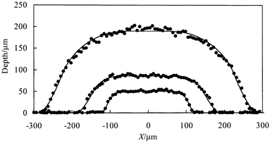 | ||
| Fig. 11 Channel cross sectional profiles for chip bases with etch times of (in order of increasing depth) 24, 48 and 120 min. The solid curves are best-fits to the model described in the text with the parameters listed in Table 1. | ||
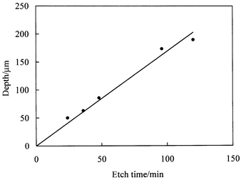 | ||
| Fig. 12 Variation of channel depth with etch time under the conditions described in the text. The solid line corresponds to a mean etch rate of 1.7 µm min−1. | ||
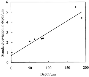
For each of the different chip bases, we have determined the standard deviation in channel depth over the flat region of the channels around the channel centre. The observed variability in channel depth can result from two causes. Firstly, variation can result from the random uncertainty in the microscope absorbance measurements and hence in the measured depths. Secondly, the channel surfaces may actually be rough giving a real point-to-point variation in depth. Fig. 13 shows a plot of the standard deviation in depth versus depth. The slope of the plot corresponds to the uncertainty (one standard deviation) in depth being 2.3% of the measured depth. This level of uncertainty is reasonably consistent with the value expected from the analysis shown in Fig. 4. The intercept of Fig. 13 suggests that the actual roughness of the channel surfaces is of the order of 0.7 µm. Although plausible, the ‘scatter’ of the data of Fig. 13, makes this estimate rather uncertain.
 | ||
| Fig. 13 Standard deviation in channel depth versus depth. The solid line corresponds to an uncertainty (one standard deviation) of 2.3% of the channel depth plus an intrinsic depth variability of 0.7 µm given by the intercept of the plot. | ||
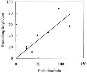
Finally, Fig. 14 shows the variation of fitted smoothing length δversus etch time. Although the uncertainty in δ is large, the results suggest that the distortion away from the ideal isotropic etch profile increases with increasing etch time.
 | ||
| Fig. 14 Variation of fitted smoothing length δ with etch time. | ||
Conclusions
We have developed a rapid, accurate and non-destructive technique to determine the 3D profiles of microreactor channel networks based on optical imaging of dye filled channels. The method is capable of measuring channel depths from 10 to 500 µm (and probably smaller depths) with an accuracy of a few percent and a spatial resolution of less than 1 µm. It has been established that distortion of the measured profiles resulting from a mismatch in refractive index between the dye solution and the glass of the microreactors are insignificant. The method has been successfully used to investigate the effects of thermal bonding and etch time on channel profiles.The imaging method developed here could be applied to profile any solution-fillable voids within transparent solids. Furthermore, for microreactor channels where the depth (path length) has been measured, the technique may also be applied to determine the concentration profiles of either absorbing or fluorescent species in the channels with a time resolution of greater than 10 frames per second. This aspect is currently under active investigation in our laboratories.
Acknowledgements
We thank the Engineering and Physical Sciences Research Council of the UK for funding this study and the Institute of Applied Catalysis (iAC) for partial funding of the Studentship for Ian Broadwell.References
- S. J. Haswell, R. J. Middleton, B. O’Sullivan, V. Skelton, P. Watts and P. Styring, Chem. Commun., 2001, 391 RSC .
![[*]](https://www.rsc.org/images/entities/char_e103.gif) This feature article gives a clear account of current work on synthesis in microreactors.
This feature article gives a clear account of current work on synthesis in microreactors. - V. Skelton, G. M. Greenway, S. J. Haswell, P. Styring, D. O. Morgan, B. H. Warrington and S. Y. F. Wong, Analyst, 2001, 126, 7 RSC.
- V. Skelton, G. M. Greenway, S. J. Haswell, P. Styring, D. O. Morgan, B. H. Warrington and S. Y. F. Wong, Analyst, 2001, 126, 11 RSC .
This paper describes the first demonstration of the control of stereoselective product formation
in a microreactor.
- G. N. Doku, S. J. Haswell, T. McCreedy and G. M. Greenway, Analyst, 2001, 126, 14 RSC.
- T. McCreedy and N. G. Wilson, Analyst, 2001, 126, 21 RSC.
- M. C. Mitchell, V. Spikemans and A. J. de Mello, Analyst, 2001, 126, 24 RSC.
- P. D. I. Fletcher, S. J. Haswell and V. N. Paunov, Analyst, 1999, 124, 1273 RSC .
This tutorial review gives a clear account of the underlying principles of chemical reaction control in microreactors.
- T. McCreedy, Trends Anal. Chem., 2000, 19, 396 CrossRef CAS.
- T. McCreedy, Anal. Chim. Acta, 2001, 427, 39 CrossRef CAS.
- P. J. Treado, A. Govil, M. D. Morris, K. D. Sternitzke and R. J. McCreery, Appl. Spectrosc., 1990, 44, 1270 CAS.
- S. C. Jacobson, R. Hergenroder, L. B. Koutny, R. J. Warmack and J. M. Ramsey, Anal. Chem., 1994, 66, 1107 CrossRef CAS.
- J. Wu and J. Pawliszyn, Anal. Chem., 1994, 66, 867 CrossRef CAS.
- E. N. Lewis, P. J. Treado, R. C. Reeder, G. M. Story, A. E. Dowrey, C. Marcott and I. W. Levin, Anal. Chem., 1995, 67, 3377 CrossRef CAS.
- Z. Wang and D. Scherson, J. Electrochem. Soc., 1995, 142, 4225 CAS.
- E. T. Bergstrom, D. M. Goodal, B. Porkric and N. M. Allinson, Anal. Chem., 1999, 71, 4376 CrossRef.
- B. L. McClain, J. Ma and D. Ben-Amotz, Appl. Spectrosc., 1999, 53, 1118 CrossRef CAS.
| This journal is © The Royal Society of Chemistry 2001 |