Rapid fabrication of microfluidic devices in poly(dimethylsiloxane) by photocopying†
Aimin
Tan‡
a,
Kenneth
Rodgers
b,
John P.
Murrihy
a,
Cian
O’Mathuna
b and
Jeremy D.
Glennon
*a
aMicroseparations Laboratory, Analytical Chemistry, Department of Chemistry, National University of Ireland, Cork, Ireland. E-mail: j.glennon@ucc.ie; Fax: +353 21 4274097
bNational Microelectronics Research Center, Lee Maltings, Cork, Ireland
First published on 9th August 2001
Abstract
A very simple and fast method for the fabrication of poly(dimethylsiloxane) (PDMS) microfluidic devices is introduced. By using a photocopying machine to make a master on transparency instead of using lithographic equipment and photoresist, the fabrication process is greatly simplified and speeded up, requiring less than 1.5 h from design to device. Through SEM characterization, any µ-channel network with a width greater than 50 µm and a depth in the range of 8–14 µm can be made by this method. After sealing to a Pyrex glass plate with micromachined platinum electrodes, a microfluidic device was made and the device was tested in FIA mode with on-chip conductometric detection without using either high voltage or other pumping methods.
Introduction
There is a growing interest in the miniaturization of analytical systems in recent years owing to the advantages of fast analysis time, portability, disposability, reduced consumption of reagents, and better performance.1–3 Both the microfabrication techniques and materials in IC industry have been extensively used for this purpose. Despite the great successes,2–5, more and more efforts are being made to find out alternative microfabrication methods and materials for lower cost, easier and quicker fabrication.6,7 Poly(dimethylsiloxane) (PDMS) is a very attractive material for microfluidic devices. It has been widely used in several microfabrication or nanofabrication methods collectively known as soft lithography.8 PDMS has been used to fabricate microchip electrophoresis systems employing laser-induced fluorescence (LIF)7,9 and amperometric detection.10 It was also used to fabricate microfluidic devices for picoliter liquid sample handling,11 sample delivery in mass spectrometry (MS),12,13 and even to make complex three-dimensional microfluidic systems.14While making a PDMS device, a master is firstly fabricated and then the PDMS prepolymer mixture is cast over the master and cured. Although it is fast to make a replica in PDMS, the master fabrication is relatively time-consuming. Photoresists and mask aligner equipment, even silicon etching facilities are used, which are not widely available. Though making replicas rapidly is important, rapid fabrication of a master is much more important, especially during the early stage of testing new concepts in microfluidic systems. Efforts to minimize the need for specialized equipment, such as using an office printer and photographic reduction, have been reported.15 In this paper, a master is made on transparency using a photocopying machine, thus greatly decreasing the total fabrication time (less than 1.5 h). The result is a simple user-friendly method of preparation of microfluidic channels in PDMS. To the best of our knowledge, this is the fastest and simplest method to date to make a microfluidic device in PDMS. The PDMS microfluidic devices made by this method were characterized by SEM and tested in FIA mode with on chip conductive detection without using high voltage or other pumping methods.
Experimental
Materials and reagents
The following chemicals and materials were used as received: Sylgard® 184 Silicon Elastomer (Dow Corning, USA), Victoria blue B (Fluka Chemika, Switzerland), sodium chloride, and ethanol (Labscan, Ireland).Fabrication
Designs of networks of microfluidic channels were firstly generated by using a computer drawing package. After being printed out, the pattern was transferred onto a transparency to make a master using a photocopying machine. Next, a 10∶1 mixture of PDMS prepolymer and curing agent was cast over the master with a frame for holding the solution and cured for 1 h at 65 °C. After curing, the PDMS replica was peeled from the master and holes were punched on the PDMS replica for reservoirs. The whole process from design to replica took less than 1.5 h. The PDMS replica was then sealed to a Pyrex glass plate by adhesion to make a microfluidic device. The channel dimensions are 55 mm (length), 200 µm (width), and 12 µm (depth). On the glass plate, two platinum electrodes have been micromachined by photolithography and rf plasma sputtering as described previously.16 Electrical wires were glued to the platinum electrodes using Ablebond 967-1 conductive epoxy glue (Ablestick, Cambridge, UK) and were connected to a PED-1 pulsed electrochemical detector (Dionex Corp., California, USA) for conductometric detection.Results and discussion
Fig. 1 shows the cross section of a µ-channel on PDMS. Its shape is trapezoidal, similar to those on glass fabricated by isotropic etching.17,18 However, the underlying reason for producing trapezoidal shape channel is different from isotropic etching. In this case, the shape is based on a gathering of many carbon particles, which have a natural tendency to form a round curve at the edges. The channel depth depends on how thickly the carbon particles have been deposited on a transparency while photocopying. By setting the darkness in the photocopying machine, it is possible to control the depth of the channel. When using the most common darkness settings in the middle region, the channel depth is usually in the range of 8 to 14 µm. In order to make deeper channels, higher darkness settings may be used. However, if the quality of the photocopying machine is not very good, black spots on white area (the area without designed channel or other structure) may be observed, which may produce unwanted pattern in unused area or in some cases distort the pattern. The µ-channel width formed on a PDMS replica depends both on the width in the design and the reduction or enlargement ratio used while photocopying. As a routine desktop printer, instead of high precision printer, was used to print out the design, the pattern was photographically reduced 4 times while photocopying. As shown by SEM results, any channel with a width greater than 50 µm can be readily made by this method.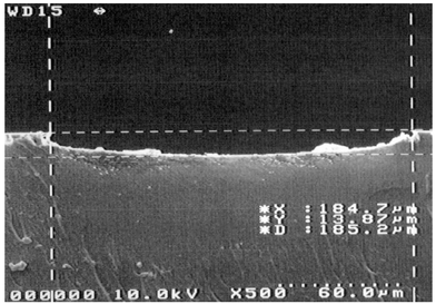 | ||
| Fig. 1 SEM image of cross section of the channel on PDMS. | ||
Fig. 2 shows an intersection in a PDMS device, which is a typical structure used in microfluidic systems for fluid switching or sample injection. As the master is based on relief pattern by carbon particles deposited on a transparency, the walls of molded polymer are not as smooth as those using photoresist or silicon based masters. Finer carbon particles may be used to reduce channel roughness. However, as shown by others,7 channel roughness did not have any significantly adverse effects on the performance of a device while working in the very common electroosmotic or electrophoretic mode. The silanization of a master is not necessary and the master can be used more than once. Since it is very fast from a design to a replica, this method is very useful in rapid testing and selection of new concepts in microfluidics.
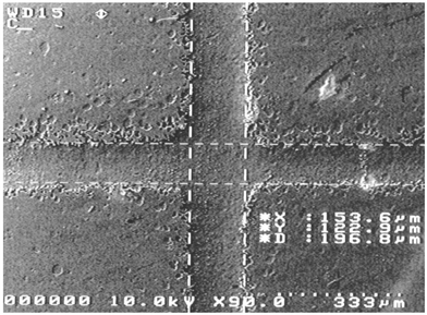 | ||
| Fig. 2 SEM image of a channel intersection on PDMS. | ||
PDMS has very good physical–chemical properties, including (1) high optical quality, transparent above 230 nm; (2) high electrical bulk resistivity; (3) good chemical stability; (4) support for electroosmotic flow (EOF) after plasma oxidation and (5) good adhesion to a variety of clean and flat substrates.7,9 PDMS microchips working in capillary electrophoresis (CE) mode with LIF or amperometric detection have been well documented.7,9,10 PDMS microfluidic devices were compatible with MS detection.12,13 As similar devices (cross or double-T shaped channels) have been made by this method, it is quite possible that similar results could be obtained if tested in the same way. Therefore, an initial test was carried out with a single channel PDMS chip (length: 55 mm; width: 200 µm; depth: 12 µm), made here to test its microfluidic performance and analytical utility. A small droplet of a standard sample mixture (10 mM sodium chloride and 5 mM Victoria blue B) was placed at the µ-channel inlet to allow a 1–2 mm length of sample segment, about 2–4 nl, to enter the µ-channel by capillary action. Then a larger µl volume of ethanol, as mobile phase, was placed over the channel inlet, which propelled the sample segment through the channel to the platinum electrodes by capillary action, resulting in a sharp FIA peak (Fig. 3). This microfluidic test was achieved without using a high voltage power supply or any other pumping method.
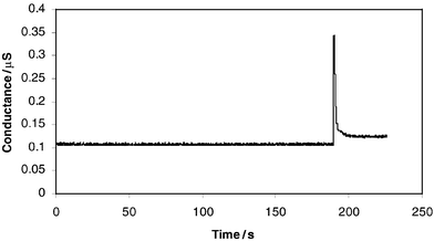 | ||
| Fig. 3 FIA in microfluidic device with on-chip conductivity detection. | ||
Conclusions
A simple and fast way to fabricate PDMS microfluidic devices is established. Even though the walls of the molded polymer are less smooth as compared to those molded against masters created by micromachining silicon or developed photoresists, it should be very useful for quick testing of new ideas in microfluidics. The preliminary test shows the analytical applicability. As neither high voltage power supply nor other pumping methods were used in the test, the results show great potential in developing real portable, disposable µTAS devices. More tests are in progress.References
- A. Manz, J. C. Fettinger, E. Verpoorte, H. Ludi, H. M. Widmer and D. J. Harrison, Trans. Anal. Chem., 1991, 10(5), 144 Search PubMed.
- F. E. Regnier, B. He, S. Lin and J. Busse, Trends Biotechnol., 1999, 17, 101 CrossRef CAS.
- D. Figeys and D. Pinto, Anal. Chem., 2000, 72, 330A CAS.
- S. C. Jacobson, C. T. Culbertson, J. E. Daler and J. M. Ramsey, Anal. Chem., 1998, 70, 3476 CrossRef CAS.
- A. T. Woolley, G. F. Sensabaugh and R. A. Mathies, Anal. Chem., 1997, 69, 2181 CrossRef CAS.
- M. A. Roberts, J. S. Rossier, P. Bercier and H. Girault, Anal. Chem., 1997, 69, 2035 CrossRef CAS .
![[*]](https://www.rsc.org/images/entities/char_e103.gif) A UV laser photoablation method for creating microfluidic systems on polymer substrates is described and the work highlights the necessity of finding alternative fabrication methods and materials for miniaturized systems.
A UV laser photoablation method for creating microfluidic systems on polymer substrates is described and the work highlights the necessity of finding alternative fabrication methods and materials for miniaturized systems. - D. C. Duffy, J. C. McDonald, O. J. A. Schueller and G. M. Whitesides, Anal. Chem., 1998, 70, 4974 CrossRef CAS .
These authors describe a procedure that makes it possible to design and fabricate microfluidic system in PDMS in less than 24 h. The main improvement is to create a master in positive relief photoresist, other than in silicon, thus greatly speeding up the fabrication. It is most relevant because our paper also concerns master creation by simpler methods.
- S. Brittain, K. Paul, X.-M. Zhao and G. Whitesides, Phys. World, May 1998, 31 Search PubMed.
- C. S. Effenhauser, G. J. M. Bruin, A. Paulus and M. Ehrat, Anal. Chem., 1997, 69, 3451 CrossRef CAS .
This is the first paper to make microfluidic channels on PDMS using etched silicon as a master.
- R. S. Martin, A. J. Gawron and S. M. Lunte, Anal. Chem., 2000, 72, 3196 CrossRef CAS.
- K. Hosokawa, T. Fujii and I. Endo, Anal. Chem., 1999, 71, 4781 CrossRef CAS .
A picoliter sample-handling device fabricated in PDMS is described, which is a good representative example of the utility of PDMS based microfluidic devices.
- J. H. Chan, A. T. Timperman, D. Qin and R. Aebersold, Anal. Chem., 1999, 71, 4437 CrossRef CAS.
- H. Liu, C. Felten, Q. Xue, B. Zhang, P. Jedrzejewski, B. L. Karger and F. Foret, Anal. Chem., 2000, 72, 3303 CrossRef CAS.
- J. R. Anderson, D. T. Chiu, R. J. Jackman, O. Cherniavskaya, J. C. McDonald, H. Wu, S. H. Whitesides and G. M. Whitesides, Anal. Chem., 2000, 72, 3158 CrossRef CAS.
- T. Deng, H. Wu, S. T. Brittain and G. M. Whitesides, Anal. Chem., 2000, 72, 3176 CrossRef CAS.
- M. McEnery, A. Tan, J. Alderman, J. Patterson, S. C. O’Mathuna and J. D. Glennon, Analyst, 2000, 125, 25 RSC .
This paper from our research team, describes the successful
fabrication of an LC on-chip system in silicon and glass with on-chip injection, separation, and electrochemical detection.
- Z. H. Fan and D. J. Harrison, Anal. Chem., 1994, 66, 177 CrossRef CAS.
- S. C. Jacobson, A. W. Moore and J. M. Ramsey, Anal. Chem., 1995, 67, 2059 CrossRef CAS.
Footnotes |
| † Presented at the 14th International Symposium on Microscale Separations and Analysis, Boston, January 13–18, 2001. |
| ‡ On leave from the Department of Chemistry, Central South University, Changsha 410083, China. |
| This journal is © The Royal Society of Chemistry 2001 |