Dielectric materials for applications in microwave communications†
R. J. Cavaab
aBell Laboratories, 600 Mountain Avenue, Murray Hill, NJ 07974, USA
bPrinceton Materials Institute and Department
of Chemistry, Princeton University, Princeton, NJ 08540, USA
First published on 10th October 2000
Abstract
Dielectric ceramic materials have been studied for decades due to both their application in important technologies and the fundamentally interesting relationships among their crystal chemistry, crystal structures, and physical properties. Recent dramatic changes in microelectronics and in particular wireless communications technologies have made the importance of materials with the unusual combination of high dielectric constant, low dielectric loss and low temperature dependence of dielectric constant of great interest. In this review, the present state of knowledge of the chemistry, structure, and dielectric properties of these materials, as well as examples of our own work, are described.
Introduction
The revolution in wireless communications and information access is one of the most dramatic changes in technology in the past decade. This revolution is apparent on a daily basis in the ever increasing number of cellular telephone users. As in all technological systems, at the basis of the revolutionary changes in wireless communication technology are advances in materials. These materials are in use in the circuitry which wireless devices have in common with other microelectronics based technologies, but are also in use in parts of the technology which are distinctly different from those found in other systems. These unique technologies demand materials which have their own specialized requirements and functions. The importance of miniaturization cannot be overemphasized in any hand-held communications application, and can be seen in the dramatic decrease in the size and weight of devices such as cellular telephones in recent years. This constant need for miniaturization provides a continuing driving force for the discovery and the development of increasingly sophisticated materials to perform the same or improved function with decreased size and weight.Of particular interest to materials chemists are the dielectric materials used as the basis for resonators and filters for the microwaves carrying the desired information. These materials are presently employed as bulk ceramics in microwave communication devices; they are not integrated into the microelectronics but are found as discrete components. The ceramic pieces are designed to be dielectric resonators, resonating at the frequency of the carrier signal to allow that signal to be efficiently separated from other signals in the microwave band.1 The resonant frequency of the dielectric component depends on the dielectric constant of the dielectric and the size of the resonator. Looked at from another point of view, the size of the resonator at any particular resonant frequency depends on the inverse of the square root of the dielectric constant of the dielectric, and thus the larger the dielectric constant the smaller the ceramic component needed. Compared to a vacuum cavity, for example (K = 1) a dielectric with K = 36 will have the same resonant frequency at 1/6 the size.2 Thus materials with the highest possible dielectric constant would seem to be optimal for the task.
Unfortunately, there are other requirements for the resonator which make
almost all materials with high dielectric constant such as ferroelectrics
impossible to use for these applications. To be useful, the resonant frequency
of the filters must not depend strongly on temperature. If that frequency
were to be temperature dependent, then the carrier signal would drift in and
out of resonance on hot and cold days. The practical requirement is that for
a temperature range from approximately −40 to 100![[thin space (1/6-em)]](https://www.rsc.org/images/entities/char_2009.gif) °C, the
change in resonant frequency as a function of temperature (TCF)
should be less than 10 ppm °C−1. The TCF
is related to the temperature coefficient of the dielectric constant, TCK,
by: TCF = −1/2 TCK − α,
where α is the thermal expansion coefficient.3
Thus TCF is dominated by TCK, which can typically occur in the range of −2000
to +2000 ppm °C−1 in common dielectric
materials. This is an extremely stringent restriction, especially on materials
with dielectric constants larger than about 30, resulting in the fact that
very few materials are potentially usable in such applications.
°C, the
change in resonant frequency as a function of temperature (TCF)
should be less than 10 ppm °C−1. The TCF
is related to the temperature coefficient of the dielectric constant, TCK,
by: TCF = −1/2 TCK − α,
where α is the thermal expansion coefficient.3
Thus TCF is dominated by TCK, which can typically occur in the range of −2000
to +2000 ppm °C−1 in common dielectric
materials. This is an extremely stringent restriction, especially on materials
with dielectric constants larger than about 30, resulting in the fact that
very few materials are potentially usable in such applications.
Further, to optimize the signal intensity and the number of channels possible within a given frequency range, the loss of the resonator must be low. This in turn requires that the dielectric loss in the microwave frequency range (about 500 MHz to 20 GHz) of the dielectric material should be very low, with quality factor (Q), [defined as 1/(dielectric loss tangent)], better than 1000, preferably an order of magnitude higher. This requirement eliminates the use of many conventional high dielectric constant materials such as ferroelectrics.
These requirements: high dielectric constant, low temperature coefficient of dielectric constant, and low dielectric loss, are almost always mutually exclusive in dielectric materials. Further, the demands of mass production of the devices require reliable, reproducible processing of the ceramics, with tolerances of only a fraction of a ppm °C−1 in TCK and 1% in dielectric constant from one component to the next. These stringent requirements make the development of advanced materials for microwave communications a challenging area of research, especially since many of these attributes are only poorly understood from a first principles viewpoint. In fact only a few such materials are known. Some of these are described briefly in this report. Due to the lack of detailed understanding of the fundamental physics which give rise to losses in bulk polycrystalline ceramics and the temperature coefficient of the dielectric constant in the microwave frequency range (described briefly below), the discovery of such materials is virtually completely empirical. There are other brief reviews,3 and a modest book available4 on this topic, and some authors (e.g. P.K. Davies at the University of Pennsylvania) have many publications in this area. In spite of its importance, it is not widely described in non-proprietary literature, and not broadly funded outside corporate research laboratories. In the following sections, some aspects of the most well known high K, high Q, low TCK dielectric materials are described, along with some of our own exploratory work in this area. This article concentrates almost exclusively on the materials chemistry of low TCK dielectric ceramics. Equally essential to understanding their observed properties are the effects of microstructure and processing, which are described here for some cases, but not extensively. A comprehensive review of that aspect of the field, by an expert in ceramic processing, would be of great interest.
(Zr1 − xSnx)TiO4—zirconium tin titanate
This material, on the surface appearing relatively simple, but in fact very complex, is widely employed in microwave devices. Many of the issues faced in the understanding of the relationship between the dielectric properties and the detailed crystal structure of this compound are in fact surprisingly common to many of the other compounds in this small family of materials, even when they are based on entirely different structure types. The basic compound, ZrTiO4, has long been known to have a relatively low temperature coefficient of the dielectric constant,3 but has been found to have optimal properties, K ≈ 38, TCF <10 ppm °C−1, and Q ≈ 5000–10,000 at microwave frequencies, for solid solutions involving partial substitution of Sn4+ for Zr4+ at the 20% level.5The crystal structure is of the α-PbO2 type, shown
in Fig. 1, based on columns of zigzag
chains of edge shared metal–oxygen octahedra, two octahedra wide. These
columns share corner oxygens with columns in the next metal plane in a close-packed
oxygen lattice.6 For materials heated at 1200°C
and higher, the entropic contribution to the total energy of the crystal is
dominant, and Zr and Ti are fully disordered, randomly mixed on the octahedral
metal sites. At low temperatures, however, the differences in coordination
environments expected from Pauling’s rules—that Ti should have
octahedral coordination to oxygen and Zr cubic coordination—overcome
entropy, and an ordered crystal structure is formed. In the ordered structure,
the columns of edge shared metal–oxygen polyhedra are either exclusively
TiO6 octahedra or distorted ZrO8 cubes formed by slight
local shifts of the close-packed oxygens.6
The Ti and Zr edge shared columns alternate. The distortion of the close-packed
oxygen lattice which occurs during the cation ordering results in the shortening
of one of the crystallographic axes, an easily observable change often taken
as the primary indicator that such ordering has occurred. The ordering transition
is sluggish, occurring on the time scale of typical ceramic processing procedures (hours)
and therefore processing parameters such as the cooling rate can have an important
influence on the exact nature of the phase obtained. Further, it has been
shown that there are more complex partially ordered states between the fully
ordered and disordered variants involving different TiO6–ZrO8
column sequences in materials dependent on cooling rate and exact Zr/Ti
ratio.6
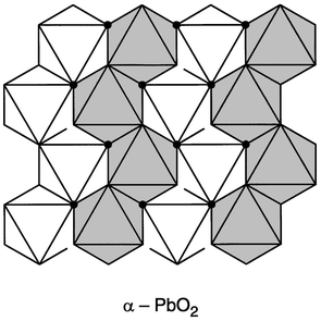 | ||
| Fig. 1 The crystal structure of ZrTiO4, the α-PbO2 type. The shaded and unshaded metal–oxygen octahedra are above and below the close packed plane of oxygen atoms in the plane of the paper. In the disordered variant, Zr and Ti are mixed on all metal sites. In the ordered variant, columns of octahedra are occupied by either Zr or Ti, with an accompanying distortion of the oxygen array. | ||
The crystallographic form of ZrTiO4 influences the dielectric
properties to a small but significant degree. In one controlled experiment,6 for pure ZrTiO4 prepared at high temperature,
where the Zr and Ti are fully disordered, the dielectric properties at microwave
frequencies were found to be: K = 43, TCK = 58 ppm °C−1,
and Q = 3100, and for samples annealed for a long
time at 1050°C, showing a well ordered Zr/Ti array, the properties
were found to be K ≈ 38, TCK = 76 ppm °C−1,
and Q ≈ 2100. Contrary to the generally negative influence
of disorder3,5 the Q value is
larger in the disordered material, indicating the influence of other factors,
not yet understood. Changes in K, Q, and TCK are observed
in other dielectric systems as well as a function of cation disorder, an apparently
generic characteristic of this class of materials. The influence of disorder
on the properties of pure ZrTiO4, however, is less pronounced than
what is generally observed.
Though the effect of Zr/Ti disorder is significant, it is not as dramatic as partial Sn substitution for Zr. This substitution results in a sufficient decrease in TCK to allow the practical use of this material. As all the elements are tetravalent, it is possible over a small composition range to have mixed substitution of Sn for both Ti and Zr, resulting in a general formula Zr1 − xTi1 − ySnx + yO4. However the best properties are obtained for materials with pure Zr substitution Zr1 − xSnxTiO4, where the solid solution range is approximately 0.0 < x < 0.4. At compositions between x = 0.2 and x = 0.3, both the lowest TCF (1–5 ppm °C−1) and highest microwave frequency Q values (7000–10,000) are obtained.5 It is certainly surprising that both these important qualities are optimized near the same composition, as no microscopic connection between Q and TCF has thus far been established.
The effect of the Sn substitution on the crystal structure has been studied in an attempt to correlate the structure and the dielectric properties.6 In general, the addition of a third metal element to a material like ZrTiO4 would be expected to facilitate the occurrence of the disordered state, as partial mixing increases entropy and should therefore stabilize the more disordered phase. This is true for this system on averaging over many unit cells, but the true microscopic structure is much more complex. The Sn substitution, at temperatures which usually result in the ordered structure, actually causes a mixing of ordered chain fragments of TiO6 octahedra with ordered chain fragments of double ZrO8 cubes along single columns which in the fully ordered structure would contain only octahedra or cubes. It has been proposed that the Sn substitutions occur at the exact locations of the switching from TiO6 octahedra to ZrO8 cubes along the chains, thus resulting in more switching in the columns (and shorter chain fragments) with increasing Sn content. Thus, the size of the regions of ordered octahedra and cubes decreases with increasing Sn content. This decrease in the correlation lengths of the ordered regions occurs with the increasing Sn content, as does the increase in Q and decrease in TCF. It has also been shown that for a fixed Sn content, increased annealing time at low temperatures increases the Q value.3 Since annealing is expected to decrease disorder, it is possible that its actual affect is to make the lengths of the ordered chain fragments in the mixed columns more uniform within the overall average structure, through more uniformly distributing the substituted Sn at the interfaces between Ti rich and Zr rich regions. It has been proposed (though not proven) that this short-range ordering of the Sn is what improves the Q values.6 Why such a complex local structure should decrease the TCK at the same time for this material has not been established. Due to the commercial significance of this material and its interesting crystal chemistry many other studies have been performed which test the effects of chemical additions and substitutions on the processing and properties of bulk dielectrics. Examples of these types of studies can be found in references 7 and 8. Though of interest, none of these chemical additions appear to greatly improve either the processing or properties of the basic (Zr,Sn)TiO4 solid solution.
Ba(Zn1/3Ta2/3)O3 and related perovskites
These perovskites are of particular interest for microwave applications because they can be fabricated with exceptionally high Q values at microwave frequencies (see, for instance, refs. 9–14). Although the K values (25–30) are lower than those obtained for the (Zr,Sn)TiO4 dielectrics, they do have low TCF values (<5 ppm °C−1) and remarkably high Q values, in the range of 10,000–40,000. The high Q values in the pure materials are obtained after annealing at high temperatures for very long times, of the order of 100 hours at 1400°C, conditions incompatible with reasonable commercial
manufacturing practices. The long annealing times necessary to obtain high Q
value materials indicates, as for (Zr,Sn)TiO4, that order/disorder
on the transition metal sublattice has an important effect on the dielectric
properties. Essential to the eventual commercialization of these materials
was the discovery that for small changes in composition in the (1 − x)Ba(Zn1/3Ta2/3)O3–(x)BaZrO3 perovskite
solid solution, for x < 0.05, the heating time necessary
at high temperatures to obtain the high Q state was reduced by a
factor of 10. As in the case of (Zr,Sn)TiO4, a complex
relationship between local crystal structure and dielectric properties may
be inferred. For the perovskites, however, the phenomenology seems more straightforward,
making these materials of particular interest for detailed study.The crystal structure of Ba(Zn1/3Ta2/3)O3 is that of a classic ordered perovskite with two transition metals (B and B′) on the octahedral site. The most common B-site ordered perovskite structure type occurs for a stoichiometry A2BB′O6, shown in Fig. 2. The B and B′ ions occur on alternating (111) planes in a 1∶1 ratio. The ordered A3BB′2O9 structure type, where the B and B′ atoms occur in a 1∶2 ratio, which occurs for Ba(Zn1/3Ta2/3)O3, is common to other related dielectric perovskites, with, for example, Mg or Ni in place of Zn, or Nb in place of Ta.10 In the ordered form of this perovskite, as in the 1∶1 variant, the Zn and Ta octahedra are ordered in the (111) perovskite planes. Each (111) plane contains only one type of small ion–oxygen octahedron, and the planes are ordered in the 1∶2 stoichiometric proportion, in the sequence –Zn–Ta–Ta–Zn–Ta–Ta–.... The resulting symmetry, due to the (111) type plane stacking and accompanying small oxygen displacements, is trigonal. The attainment of perfect B-site ordering for the stoichiometric compounds is very sluggish. Partial disorder, which mixes the different B-site ions within single (111) planes, is very common under normal synthetic conditions, and all materials are highly disordered as initially synthesized.9 The correlation between long annealing time, improved ordering of the B-site ions, and the highest Q dielectric properties has been clearly experimentally established in these materials.9–14 The improved Q with decreased disorder is consistent with the idea that good atomic ordering decreases the frequency widths of phonon vibrations at infrared frequencies whose tails extend into the microwave region and are major contributors to the microwave frequency dielectric loss.1,3,5
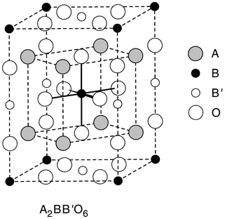 | ||
| Fig. 2 The crystal structure of one of the ordered B-site perovskite structure types found for dielectric materials. This illustrates the ordered perovskite of stoichiometry A2BB′O6, with B and B′ planes alternating in a 1∶1 ratio along the perovskite subcell (111) direction. In the ordered A3BB′2O9 variant found for Ba(Zn1/3Ta2/3)O3 the Zn and Ta occur in (111) planes alternating in a 1∶2 ratio. These two structure types compete energetically in Ba(Zn,Ta,Zr)O3 low TCK dielectrics. | ||
So in this system everything seems to make sense until one considers what effect the solid solution with the BaZrO3 perovskite might have on the dielectric properties. The addition of an additional B-site element is expected to encourage disorder on that sublattice, and such disorder has been deduced to occur based on the disappearance of the superlattice ordering reflections in conventional X-ray diffraction experiments. This disorder would have the effect of decreasing rather than increasing the Q values according to the picture of disorder broadened phonon frequency resonances. The opposite effect in fact occurs, with only 10 hours annealing time needed to attain the high Q state. As was found to be the case in (Zr,Sn)TiO4, the full story involves local atomic ordering and is quite complex.
Because trigonal Ba(Zn1/3Ta2/3)O3 is based on small distortions of a cubic perovskite cell, there are eight possible unique (111) directions which can become the unique trigonal axis when the low symmetry phase forms out of the disordered cubic phase during ordering. Thus in crystals of Ba(Zn1/3Ta2/3)O3 there are twin domains with eight different orientations. The dimensions of these domains can be seen with an electron microscope, and are on the order of 2000 angstroms in the well ordered non-Zr doped material.10 The domains are separated by domain boundaries. The ordering involves the growth of these ordered domains from the disordered B-site arrangement. For small levels of Zr doping, on the 1–3% doping level, these domains can still be seen, but decrease radically in dimension, becoming on the order of 25–50 angstroms in size. Thus the apparent disorder deduced to occur on Zr doping of Ba(Zn1/3Ta2/3)O3 from conventional X-ray diffraction experiments is an incorrect conclusion—the extra peaks due to Zn/Ta ordering become weak and broad because the domain sizes get very small.10 The possible explanation of the increased kinetics in the formation of the high Q state can then be explained as being due to the fact that the ordering times for forming these small domains of ordered material are much shorter than for forming the larger domains in the undoped material. However such small domains result in a larger relative volume of material in domain boundaries, which are expected to be dielectrically lossy. It has been speculated that the doped Zr in fact segregates to the domain boundaries, “stabilizing” them against lossy resonances. Further, when the doping level reaches 5%, the nature of the short-range ordering changes, from one of a tripled perovskite: B–B′–B′–B–B′–B′, to one of a doubled perovskite: B–B′–B–B′– (Fig. 2). For the doubled perovskite, the B-site layers are no longer expected to be purely one atom type or another, but rather involve some mixture. This change in ordering type near 5% substitution has been suggested to be the origin of the discontinuous change in Q at low doping levels.10
Due to the commercial importance of these materials, there have been a variety of studies of the effects of doping on the observed properties. Complex structure–property relationships have been observed.11–14 The related solid solution system CaTiO3–Ca(Al1/2Ta1/2)O3 has been reported to have a high dielectric constant (K ≈ 46) low TCF (0 ppm °C−1 for some compositions and annealing conditions) and reasonable microwave frequency Q values (1000–4000).15 The relatively high K value makes this material of particular interest. The dielectric properties for this system are again significantly affected by annealing time and temperature, suggesting that order/disorder on the B-site is important. A more complex perovskite system, (Pb,Ca)(Fe,Nb,Sn)O3, has been reported to have a very high dielectric constant (K ≈ 85–90), low TCF (near 0 ppm °C−1) and moderate microwave frequency Q value (between 500–1500),16 which is also worthy of further consideration for practical applications. It is of interest to note that for this system as well, the highest microwave Q and lowest TCF are reported to occur at the same composition and annealing conditions. No microscopic investigation of structure–property relations has been reported in either of these two cases.
As can be surmised from the preceding discussion, the detailed relationships among the temperature coefficient of the dielectric constant, chemistry, and crystal structure in complex perovskites are themselves very subtle and complex. However, from a global point of view, an overall empirical correlation between the temperature coefficient of the dielectric constant and the crystal structure, through the perovskite tolerance factor, has been established (Fig. 3).17 Recall that the tolerance factor is a measure of the relative sizes of the AO and BO2 layers, t = (RA + RO)/√2 (RB+RO). t = 1 indicates a perfect size match, with t less than 1 accommodated by rotation of the metal–oxygen octahedra to create cavities of the correct size for the A cations, with accompanying structural distortions to lower symmetry. For low tolerance factor perovskites, (t < 0.97) positive TCKs of 50 ppm °C−1 or larger are observed. There is a sharp crossover to large (−200 ppm °C−1 or larger) negative TCKs in the very small t interval of 0.97 < t < 0.99 associated with an accompanying change in the type of structural distortion. The TCK then gradually becomes less negative with increasing t, approaching 0 for the largest AO layer sizes near t = 1.05. Though such an empirical correlation is not expected to explain the detailed influence of complex order/disorder phenomena on TCK or dielectric loss, nor has it yet been interpreted in terms of the underlying lattice physics, it does present an important starting point for discussion of TCK–structure correlations in these materials.
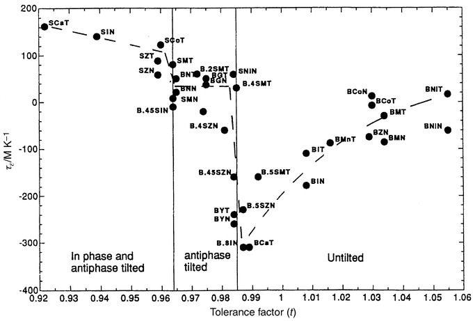 | ||
| Fig. 3 Relationship between the temperature coefficient of the dielectric constant (τε) and the tolerance factor (t) for perovskite dielectrics.17 Abbreviations employed are: B = Ba, S = Sr, T = Ta, Z = Zn, N = Nb, M = Mg, I = In, G = Gd. For details see ref. 17. | ||
As in the other dielectric family we have discussed in detail, Zr1 − xSnxTiO4, the relationships between structure and properties of the Ba(Zn1/3Ta2/3)O3 perovskite dielectrics have been well established due to careful structural analysis on the microscopic scale. However, for these cases, as well as for all others in the family of microwave frequency dielectric materials, the next step in understanding: establishing a link between the physics of the system and the observed properties and structures through experimental study, is missing. In particular, the underlying physical reason why some atomic configurations favor a low TCF and others do not has not been experimentally established. In addition, clear experimental confirmation of the proposed effect of disorder on the phonon spectra is apparently lacking. The high degree of structure–property knowledge already extant on the perovskite systems suggests that they may be excellent candidates for detailed physical study and modeling.
Barium titanates: Ba2Ti9O20, BaTi4O9, and Ba–Ln–Ti–O
The binary barium titanates were the first dielectric materials described as having practical application in modern microwave frequency resonators,18,19 and remain in commercial use. Two binary materials have good dielectric properties:2 BaTi4O9, K = 38, TCF = 14 ppm °C−1, Q > 10,000, and Ba2Ti9O20, K = 39, TCF = 4 ppm °C−1, and Q > 10,000. As in the systems described above, extensive work has been performed to test the effects of different chemical additives on the dielectric properties (see e.g.refs. 2, 20 and 21). It has been found that SnO2, ZnO or Ta2O5 additions in particular have a favorable influence in reducing the TCF for some applications. An excellent description of the many considerations involved in developing materials such as this for commercialization can be found in reference 2.The issues surrounding the chemistry/structure/property relations in this family are considerably different from those encountered in the two materials families described above. In particular, due to the simpler crystal chemistry, there are no apparent issues involving order/disorder on the Ti sublattice. The basic materials themselves as synthesized display good basic properties. Improved or altered properties on atomic substitution or change in the Ba/Ti ratio primarily appear to involve the appearance of additional phases in the ceramics. These phases in some instances may have TCFs opposing those of the majority titanates, improving the overall TCF of the ceramic. Thus multiple phase mixtures may sometimes be desirable, unlike the case for the first two systems described.
The crystal structures of these materials are more “bronze-like” than perovskite-like, and they are relatively high in Ti content. Due to the relatively lower proportion of valence-stabilizing electropositive elements such as Ba or Zr, the Q values of this family of materials are quite sensitive to firing conditions and defect chemistry. This is a result of the fact that as a consequence of this kind of crystal chemistry Ti4+ is easily partially reduced to Ti3+ under normal ceramic processing conditions in these materials, as at high temperatures oxygen vacancies may be formed. The introduction of Ti3+ decreases Q through the introduction of electrical conductivity due to electrons by the defect reaction:
 | (1) |
Important members of this family of dielectrics are related complex ternary materials in BaO–Ln2O3–TiO2 chemical systems with a bronze-like crystal structure. The compound forms for the large through intermediate size rare earths. These materials are important as they have the highest K (80–100) of all the low TCF dielectrics (TCF < 10 ppm °C−1 for some compositions) presently known. The high K comes at the cost of relatively lower Q values, in the 1000–4000 range,22 but the overall properties are acceptable for many applications. The dielectrics with the best properties consist almost exclusively of one phase, but that phase has a complex crystal structure, and until recently its exact composition was not even known. By the best current understanding, the compound is a solid solution, with formula Ba6 − 3xLn8 + 2xTi18O54. The limits of the solid solution are generally 0 < x < 0.8, and depend on lanthanide size, with optimal properties near x = 0.5.22 Nd and Sm based materials have been the most frequently studied. The solid solution involves the mixing of some of the Ba and Ln with vacancies on one crystallographic large atom site, in the appropriate ratio to maintain charge neutrality. TCF and Q are very strong functions of the composition.22 Additives such as Pb and Bi have been found to be very helpful in stabilizing the low TCK behavior,22,23 but do not have favorable effects on Q. Bi, at least, appears to substitute for the lanthanide, but the details of the crystal chemistry of Pb substitution are not yet known.
Processing of the ceramics is also an important issue.22,24 Aside from the complex crystal chemistry of this phase, the crystal structure and therefore the dielectric properties display significant anisotropy. This adds a complexity in ceramic processing not encountered in the other materials discussed thus far. The preferred crystallite orientation normally present in standard ceramic forming procedures for non equi-axial crystallites results in a bulk ceramic body whose properties are not isotropic. In particular, when fine-tuning factors such as the TCF of the ceramic sample, careful consideration of the orientation of the crystallites is necessary.22 This suggests that this material is at least partially “self-compensating” from the TCF point of view: the intrinsic TCF is likely to be different in different crystallographic directions, yielding the best TCFs for particular mixtures of orientations of the crystallites in a bulk sample.
It might be fair to say that the complexities of applying this dielectric material in as demanding an application as microwave device fabrication are a materials scientist’s worst nightmare. Unfortunately, it is important to understand all the aspects of the structure/chemistry/property relationships in this material, as it represents a unique case of a material with high K with acceptable TCF and Q. It would be discouraging if it were representative of the complexities that such materials would always have to display to be useful. For the time being, at least, it comprises a class of one and has to be taken as the best example of its kind.
Ca5TiNb2O12 perovskites, Ca2Ta2O7–Ca2Nb2O7 pyrochlores, BST–BSN, and Ta2O5–Al2O3
The materials described thus far are the most well studied microwave ceramic materials. A variety of others have been studied as well, such as those based on MgTiO3 (for example ref. 25) and the bismuthate pyrochlores (for example ref. 26). Some aspects of our own work in this family of materials are now described. We have concentrated on attempting to find single-phase high Q systems such as the perovskites described above, multiple phase systems in which TCK is balanced by mixtures of different dielectrics, and systems related to materials already in use or considered for use in the near future in thin-film based devices.We recently reported27 a new single phase dielectric perovskite to be considered for such applications. The Nb based compound, Ca5Nb2TiO12, displays a dielectric constant near 35, high quality factor (Q > 5000), and TCK <5 ppm °C−1. The TCK is highly dependent on processing conditions, indicating that order–disorder transitions on the B-site sublattice have a great effect on the dielectric properties. Unlike previously studied low TCK dielectric materials, these perovskites involve three cations in major proportion on the perovskite B-site. The chemical formula is better written as Ca4(CaNb2Ti)O12. Ca, Ti and Nb are mixed on the perovskite octahedral site in the ratio 1∶2∶1. The detailed crystal structure has not yet been determined, but the unit cell has orthorhombic symmetry with a cell volume involving multiple simple perovskite subcells. At low temperatures, the different B-site atoms may be fully or partially ordered in crystallographically inequivalent B-sites, and at high temperatures there may be more extensive disorder of atoms among the possible sites due to the influence of entropy.
The behavior of the temperature coefficient of the dielectric constant
as a function of processing temperature and time is highly unusual. There
is a double-crossing of zero TCK with processing temperature, summarized
in Figs. 4 and 5.
They present the TCK and K for both Ca5Nb2TiO12
and the related compound Ca5Ta2TiO12 for
ceramics fired for 3 hours at a set temperature, and those fired for
3 hours at low temperatures and then for 3 hours in 25°C
increments at each temperature up to the limit shown (labeled “repeat”
in the figures). At low firing temperatures, the TCK is negative, at
intermediate temperatures positive, and at high temperatures negative again.
The double zero crossing of TCK is maintained under most experimental conditions,
but it is seen that the positive TCK is not attained in the single firing
run for the niobate, although small negative values are obtained. Further
it is seen that the temperature at which the positive TCK region is reached
on heating is shifted to lower firing temperature for the repeat firing pellets.
Thus the atomic configuration which gives rise to the positive TCK state in
these materials requires a time on the scale of hours to form. This strongly
suggests that the positive TCK state is due to the formation of an ordered
state of the cations on the B-sites. This ordered state appears to be short-range
in nature, as the conventional powder X-ray diffraction patterns do not
show the appearance of new diffraction peaks in the corresponding temperature
interval. At the highest firing temperatures, the negative TCK behavior returns.
The transition temperature to this state is between 1500 and 1525 for the
niobate and 1575–1600°C for the tantalate. For both materials,
this transition occurs abruptly and is independent of firing time, suggesting
the presence of a high temperature transition from an ordered B-site structure
to a disordered B-site structure with good kinetics. Conventional powder
X-ray diffraction analysis reveals that the materials remain single-phase
perovskites, and that there has been no long-range structural rearrangement
or discontinuity in lattice parameter. As for other materials in this family,
small substitutions of another ion on the B-site, in this case Zr for Ti,
greatly influence the ordering time and temperature.28
The introduction of Zr increases greatly the temperature and time processing
windows for which a zero TCK state may be attained (Fig. 6),
enabling the eventual commercialization of this dielectric. It is expected
to display competitive properties with materials currently in use. Nothing
is yet known from a microscopic viewpoint about the short-range ordering
of the three ions on the B-site as a function of processing time and temperature.
The dramatic change from a low positive TCK state to a large negative TCK
state as a function of cation disorder in these materials suggests that they
may be excellent candidates for physical study to determine which underlying
factors determine TCK in ceramic dielectrics.
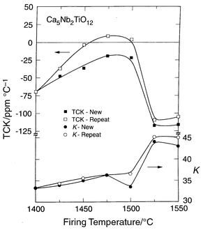 | ||
| Fig. 4 K and TCK
for Ca5TiNb2O12 as a function of firing temperature
and processing time for polycrystalline ceramics fired for 3 hours (“new”)
or multiple 3 hour firings in 25°C increments (“repeat”). | ||
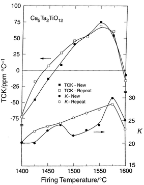 | ||
| Fig. 5 K and TCK
for Ca5TiTa2O12 as a function of firing temperature
and processing time for polycrystalline ceramics fired for 3 hours (“new”)
or multiple 3 hour firings in 25°C increments (“repeat”). | ||
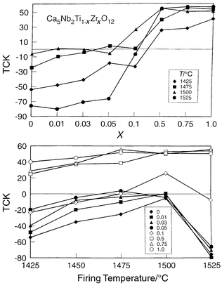 | ||
| Fig. 6 TCK for Ca5Ti1 − xZrxNb2O12 as a function of firing temperature and Zr substitution for polycrystalline ceramics fired for 3 hours, showing the improved stabilization of the low TCK phase. | ||
Interesting low loss low TCK materials may also be found among chemically related materials based on the pyrochlore structure type, Ca2Ta2O7 and Ca2Nb2O7. The dielectric data for Ca2Ta2O7: K ≅ 25, TCK ≅ −450 ppm °C−1, and for Ca2Nb2O7: K ≅ 25, TCK ≅ 250 ppm °C−1, suggest that a low TCK material can be obtained in mixtures of the two phases.29 The variation of TCK with composition across the Ca2Ta2 − xNbxO7 series is presented in Fig. 7. It is characteristic of that expected for a series in which a two-phase composition region is crossed between x = 0.2 and x = 0.4: mixing two compounds with TCK values of opposite sign. Fig. 8 depicts the sensitive dependence of TCK on composition near the balance point. The optimal material, Ca2Ta1.64Nb0.36O7, has a K of 30, TCK <2 ppm °C−1, and Q > 5000.
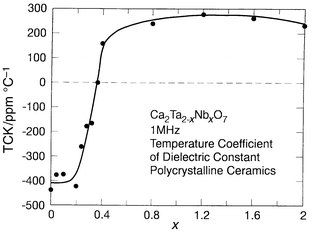 | ||
| Fig. 7 The temperature coefficient of the dielectric constant (TCK) for bulk polycrystalline ceramics of Ca2Ta2 − xNbxO7. | ||
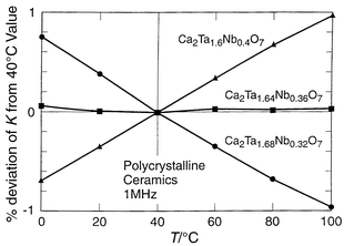 | ||
| Fig. 8 The relative change in dielectric constant in the vicinity of ambient temperature for compositions near the zero TCK value in the Ca2Ta2 − xNbxO7 system. | ||
Both Ca2Ta2O7 and Ca2Nb2O7 have pyrochlore related structure types, though they are sufficiently different that a solid solution is not formed across the Ca2Ta2 − xNbxO7 series. For x up to 0.2, the materials are a solid solution of the high temperature polymorph of Ca2Ta2O7. For x from 0.4 to 2, the materials are a solid solution of the Ca2Nb2O7 structure type. The samples in the composition region between x = 0.2 and 0.4 span the region where TCK is changing rapidly with composition, reaching a balance point near x = 0.36. At x = 0.36 a third pyrochlore related phase is dominant. It is the balance of the (small positive) TCK of that phase with the negative TCK of the Ca2Ta2O7 type solid solution phase which yields the good dielectric materials in this chemical system. Though such mixed phase systems are not as interesting from a fundamental scientific viewpoint, they do illustrate the principle that it is possible to obtain high K, low TCK, low loss microwave dielectrics in multiple phase ceramics.
The final two systems that will be described briefly were studied in attempts to change the TCKs of high K dielectric systems presently being considered as the basis of advanced capacitance components in microelectronic memory and other applications in thin film rather than bulk form. It is widely realized that further miniaturization of capacitance components in microelectronic devices requires either the fabrication of three-dimensional capacitor geometries with a high effective two-dimensional area, a complex processing issue, or the development of new dielectrics to replace SiO2. SiO2, due to its relatively low dielectric constant and limitations on the minimum thickness for which reliable layers can be fabricated, has limits for the capacitance per unit area attainable. The latter alternative requires that the new dielectric not be poisonous to the other materials in the microelectronics circuitry, and that the processing necessary to make the dielectric is compatible with microelectronics processing, two very strong restrictions.
The ferroelectric perovskite barium strontium titanate Ba1 − xSrxTiO3 (BST) has been very widely studied for use in high capacitance memory elements in microelectronics applications. Although fundamentally chemically incompatible with microelectronics, no other very high K materials (K > 300) have emerged as real alternatives. Equivalent compatibility issues also exist for other high K materials. The use of this dielectric would in fact require considerable alteration of microelectronics fabrication procedures, and it will be interesting to see whether its properties are ultimately sufficient motivation to try to work out all the processing issues its use raises.
The composition being considered for such applications, Ba0.5Sr0.5TiO3, has a peak in the temperature dependence of its dielectric constant just below room temperature. Thus the capacitance of any device based on such a material will be highly temperature dependent, making its use difficult to accommodate in circuit design. It would therefore be important to compensate for its temperature coefficient of dielectric constant without decreasing its high dielectric constant. To do so, we employed a mixed phase approach,30 as trying to alter the intrinsic properties of a dielectric to reduce its TCK would not be expected to work in ferroelectrics because very high K and low TCK are inherently exclusive. By mixing with a second ferroelectric phase in thermodynamic equilibrium with BST at this composition, with an opposite temperature dependence, it should be possible to have the two temperature dependencies partially cancel each other out. We found this to be possible in thermodynamically stable mixtures of Ba1 − xSrxTiO3 (BST) with another ferroelectric Ba1 − xSrxNb2O6 (BSN), which are in equilibrium at equal Ba∶Sr ratios. The temperature dependence of the change in dielectric constant for two-phase mixtures for bulk ceramics of this kind is shown in Fig. 9. The figure shows that the temperature dependence of the dielectric constant of BST near room temperature is largely suppressed when mixed with a large proportion of BSN. High dielectric constants are maintained in the mixture, making such materials highly preferable in applications where the capacitance of a device should be only weakly dependent on temperature.
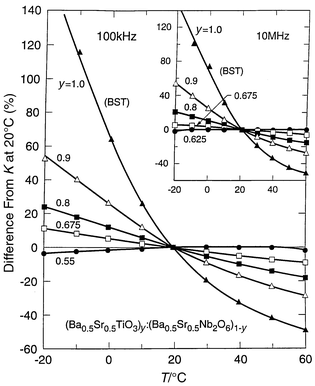 | ||
| Fig. 9 The temperature dependence
of the dielectric constant relative to its value at 20°C for multiple
phase mixtures of Ba0.5Sr0.5TiO3 and Ba0.5Sr0.5Nb2O6
in bulk ceramics. | ||
When consideration of the chemical and processing compatibility of dielectric materials with microelectronics is the primary issue, Ta2O5 emerges as the most likely near-term replacement for SiO2 in a variety of significant microelectronics applications. The dielectric constant for Ta2O5 is approximately 25 compared to 4 for SiO2. Additional important characteristics for practical application such as low leakage current, good breakdown field, and reproducible fabrication in large scale microelectronics facilities are also acceptable, and so Ta2O5 has progressed beyond the exploratory stage and into real technological development at this time.
The importance of this material for near-term application suggests that determination of the effects of processing and chemical additives on its dielectric properties is of significant interest. In that regard, we systematically explored the effects on dielectric properties of bulk ceramics of chemical additives selected from the list of elements considered fully acceptable in microelectronics processing environments. The list of such elements is highly restricted, e.g. Si, Al, Ti, N, and B and a few others.
The solid state chemistry of Ta2O5 is very interesting due to the surprising complexity of its crystal structure. The structure contains Ta in many coordination environments, suggesting that many other metals may show solubility in significant proportion. This turns out to be true for all the metals on the “allowed” microelectronics element list. Although the partial substitution of SiO2 in Ta2O5 only changes the dielectric properties as expected from an extrapolation between the end members and is therefore uninteresting, other substitutions have more dramatic effects. The partial substitution of Ti for Ta in bulk materials results in a surprising increase in K to 150 at the 8% substitution level.31 This would be an important new high K material due to its compatibility with Si processing, but attempts to fabricate thin films of partially substituted high K material by microelectronics compatible processing have so far failed to yield high dielectric constants. This may be attributable to the fact that the thin films for microelectronics are fabricated under low temperature conditions and are either microcrystalline or amorphous. The phase of Ta2O5 present in the Ti substituted bulk ceramics is the “high temperature” form, which is apparently not accessible in low temperature syntheses, even for thin films where kinetics of diffusion are expected to be very good. The possibility remains, however, that with appropriate processing the high K material may be obtained.
Of particular relevance to the topic of this review is the unexpected effect
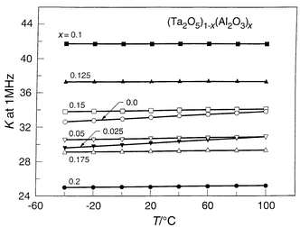
of Al2O3 partial substitutions in Ta2O5.32Fig. 10
shows the temperature dependence of the dielectric constants of (Ta2O5)1 − x(Al2O3)x solid solutions
for 0.0 < x < 0.2. Two effects can
be noted. Firstly the magnitude of the dielectric constant is not degraded
on Al2O3 substitutions in this composition range, for
example being approximately 42 at x = 0.1, even
though the K of Al2O3 itself is only 8. Secondly
it can be seen from the figure that the temperature coefficient of the dielectric
constant, normally 440 ppm °C−1, has decreased
significantly in the Al2O3 substituted materials. This
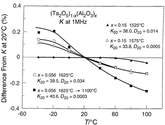
is shown in more detail in Fig. 11,
where the difference from the 20°C dielectric constant as a function
of temperature is plotted for materials with different compositions. The figure
shows that the TCK for x = 0.15 becomes very low
indeed, less than a few ppm °C−1. There apparently
have been no attempts published to date to see whether this dramatic improvement
in TCK can be seen in thin films processed under microelectronics compatible
conditions. However, because the Al2O3 substitutions
stabilize the “low temperature” form of Ta2O5,
the chances that these properties may be obtained in thin film form appear
promising. In any case, Ta2O5 is widely employed as
a bulk dielectric in other applications and the use of materials with Al2O3
addition and temperature stabilized dielectric constant may be of interest
for other applications. The relationships between the structure and crystal
chemistry of Ta2O5 and its dielectric constant and TCK
are not presently understood, nor is it apparently under study. It would be
of significant interest to characterize this material in further detail, as
the microscopic mechanisms for these effects may be of use in designing new
materials with similar properties.
 | ||
| Fig. 10 The temperature and composition dependence of the dielectric constants for Al2O3 substituted solid solutions in Ta2O5 bulk ceramics. | ||
 | ||
| Fig. 11 Detail of the relative change in dielectric constant for Al2O3 doped polycrystalline bulk ceramics of Ta2O5. | ||
Conclusions
Ceramic dielectrics with the particular combination of physical properties making them suitable for applications in microwave frequency resonators have been studied since the 1970s. For applications which require dielectric constants of 40 or less, good materials are known, though no one material at this point in time appears to have properties which are sufficiently superior to all others to dominate the commercial market. For materials with higher dielectric constants, a fundamental conflict exists at the level of the fundamental physics of materials—the atomic polarization processes necessary to achieve high dielectric constant also invariably give rise to dielectric loss and temperature dependence of the dielectric constant. Thus the development of microwave dielectric materials with dielectric constants of 75 or larger with suitable properties is in its early stages. There remains the real possibility that an exceptional material may be found on further exploration. In addition, development of specific new materials with good properties but with microelectronics compatibility will be an important step in the development of more integrated microwave/microelectronics systems. The importance of the communications and information industries to modern society certainly indicates that continued investment in the development of new materials for these applications is warranted.An added bonus in the development of these materials is the complex relationship among their chemistry, crystal structure, and dielectric properties. Several excellent studies have been done in this area, but much more remains to be learned. With the motivation of understanding materials with significant technological importance, the study of the phenomena associated with atomic order and disorder on the local scale in complex solid solution chemical systems, a topic at the forefront of current materials research, becomes of even greater interest. Further, the real details of the microscopic mechanism for the connection between the structure and properties of these materials and their physical properties have not yet been established. Collaborative efforts between materials scientists interested in dielectrics and condensed matter physicists interested in lattice dynamics and defects in solids would be very productive in helping to understand the materials now known, and would be essential in helping to find new materials with superior properties in the future.
Acknowledgement
The work at Bell Laboratories on low TCK dielectrics referred to in this review was performed in collaboration with J. J. Krajewski and W. F. Peck, Jr.References
- P. C. Osbond, R. W. Whatmore and F. W. Ainger, Br. Ceram. Soc. Proc., 1985, 36, 167 Search PubMed.
- T. Negas, G. Yeager, S. Bell, N. Coats and I. Minis, Am. Ceram. Soc. Bull., 1993, 72, 80 Search PubMed.
- R. Freer, Br. Ceram. Soc. Proc., 1995, 55, 171 Search PubMed.
- T. Negas and H. Ling eds., Materials and Processes for Wireless Communications, Ceramic Transactions 53, American Ceramic Society, Westerville, OH, 1995. Search PubMed.
- H. Tamura, Am. Ceram. Soc. Bull., 1994, 73, 92 Search PubMed.
- R. Christoffersen, P. K. Davies, X. Wei and T. Negas, J. Am. Ceram. Soc., 1994, 77, 1441 Search PubMed.
- R. Kudesia, A. E. McHale and R. L. Snyder, J. Am. Ceram. Soc., 1994, 77, 3215 Search PubMed.
- Y. Zhang and P. K. Davies, J. Am. Ceram. Soc., 1994, 77, 1743 Search PubMed.
- S. B. Desu and H. M. O’Bryan, J. Am. Ceram. Soc., 1985, 68, 546 Search PubMed.
- P. K. Davies, J. Tong and T. Negas, J. Am Ceram. Soc., 1997, 80, 1727 Search PubMed.
- M. A. Akbas and P. K. Davies, J. Am. Ceram. Soc., 1998, 81, 670 Search PubMed.
- K. Kageyama, J. Am. Ceram. Soc., 1992, 75, 1767 Search PubMed.
- M. A. Akbas and P. K. Davies, J. Am. Ceram. Soc., 1998, 81, 2205 Search PubMed.
- K. H. Yoon, D. P. Kim and E. S. Kim, J. Am. Ceram. Soc., 1998, 77, 1062 Search PubMed.
- S. Kucheiko, J.-W. Choi, H.-J. Kim and H.-J. Jung, J. Am. Ceram. Soc., 1996, 79, 2739 Search PubMed.
- S. Kucheiko, J.-W. Choi, H.-J. Kim and H.-J. Jung, J. Am. Ceram. Soc., 1997, 80, 2937 Search PubMed.
- I. M. Reaney, E. L. Colla and N. Setter, Jpn. J. Appl. Phys., 1994, 33, 3984 CrossRef CAS.
- H. M. O’Bryan, J. Thomson and J. K. Plourde, J. Am. Ceram. Soc., 1974, 57, 450 Search PubMed.
- J. K. Plourde, D. F. Linn, H. M. O’Bryan and J. Thomson, J. Am. Ceram. Soc., 1975, 58, 418 Search PubMed.
- W. Y. Lin and R. F. Speyer, J. Am. Ceram. Soc., 1999, 82, 325 Search PubMed.
- W. Y. Lin and R. F. Speyer, J. Am. Ceram. Soc., 1999, 82, 1207 Search PubMed.
- T. Negas and P. Davies, in Materials and Processes for Wireless Communications, Ceramic Transactions 53, T. Negas and H. Ling eds., American Ceramic Society, Westerville, OH, 1995, pp. 179–196. Search PubMed.
- J.-M. Wu and M.-C. Chang, J. Am Ceram. Soc., 1990, 73, 1599 Search PubMed.
- D. Suvorov, M. Valant and D. Kolar, in Materials and Processes for Wireless Communications, Ceramic Transactions 53, T. Negas and H. Ling eds., American Ceramic Society, Westerville, OH, 1995, pp. 197–207. Search PubMed.
- V. M. Ferreira and J. L. Baptista, J. Am. Ceram. Soc., 1996, 79, 1697 Search PubMed.
- M. Valant and P. K. Davies, J. Am. Ceram. Soc., 2000, 83, 147 Search PubMed.
- R. J. Cava, J. J. Krajewski and R. S. Roth, Mater. Res. Bull., 1999, 34, 355 CrossRef CAS.
- R. J. Cava and J. J. Krajewski, Mater. Res. Bull., 1999, 34, 1817 CrossRef CAS.
- R. J. Cava, J. J. Krajewski and R. S. Roth, Mater. Res. Bull., 1999, 33, 527 CrossRef.
- R. J. Cava, W. F. Peck Jr., J. J. Krajewski and D. A. Fleming, Appl. Phys. Lett., 1995, 67, 3813 CrossRef CAS.
- R. J. Cava, W. F. Peck Jr. and J. J. Krajewski, Nature, 1995, 377, 215 CrossRef CAS.
- R. J. Cava, W. F. Peck Jr., J. J. Krajewski, G. L. Roberts, B. P. Barber, H. M. O’Bryan and P. L. Gammel, Appl. Phys. Lett., 1997, 70, 1396 CrossRef CAS.
Footnote |
| † Basis of a presentation given at Materials Discussion No. 3, 26–29 September, 2000, University of Cambridge, UK. |
| This journal is © The Royal Society of Chemistry 2001 |