New optics—new materials†
Robert G. Denning
Inorganic Chemistry Laboratory, Oxford University, South
Parks Road, Oxford, UK OX1
3QR
First published on UnassignedUnassigned6th October 2000
Abstract
The nature and applications of optical materials have evolved rapidly in recent years. Their role as passive optical elements in free space has been augmented by so-called photonic systems. These can have many active components—oscillators, amplifiers, frequency converters, modulators, switches, routers and so on—most of which rely, to some degree, on optical field confinement. The design of appropriate materials for this new technology involves progress on two separate levels. There is a need both for the optimisation of microscopic electronic properties and for the separate control of bulk optical parameters on the scale of optical wavelengths. This article uses several examples to illustrate selected areas of current activity under both these headings. It also emphasises the need for more general methods for creating optical scale microstructure.
Introduction
Fifty years ago, a review of optical materials would have had a very different emphasis. The principal materials were then silicate glasses and crystals such as calcite. Their linear refraction, birefringence, and absorption were exploited, often with great ingenuity, for use in classical optical instruments, polarising components and colour filters. The shape of the field as we now know it starts to emerge in the first issue of Journal of Applied Optics in January 1962, which contains a special series of articles on optical masers (lasers). There is an interesting analogy between the evolution of optical systems and the progression from electrical circuits to electronics. In electronic systems, the functionality of networks of passive resistors, capacitors and mechanical switches is enormously enhanced by small active devices, whose properties are a function of their biasing and the currents flowing in them and whose miniaturisation has led to increased reliability and dense system integration. A similar trend in optical systems has led to the use of the term “photonics” to describe a technology, as yet only partially fulfilled, that employs active optical components to transmit and process data, largely or entirely by means of photons.Broadly, one can divide novel materials into those, such as phosphors, where the macroscopic optical homogeneity of the material is not important, and those in which the preservation of the quality of a propagating optical wavefront is significant or vital. In the latter case, the bulk optical characteristics should either be spatially uniform from the 10 nm scale upwards, to minimise Rayleigh scattering, or else precisely structured to obtain control over the optical mode structure. In practice, this means the use of fluids, glasses or single crystals. There is therefore much more to optical materials than the preparation, by methods familiar to solid state chemists, of powdered samples with suitable microscopic structural and electronic properties. It is this feature, together with difficulties implicit in growing large defect-free single crystals, that has led to a widespread interest in organic and organometallic materials. In particular, glassy polymers lend themselves to the fabrication of waveguides and integrated optical systems.
Here, my objective is a survey, from the viewpoint of a materials scientist, of some selected areas of current progress. For this purpose, I use a range of examples; from cases where the microscopic electronic structure is central, to others where the importance of the structure of the material on the scale of optical wavelengths requires new methods of fabrication.
Novel lanthanide phosphors
In addition to their application in solid state lasers, very large markets exist for lanthanide ions in colour display screens and fluorescent light tubes. The high quantum efficiency of emission that underpins these applications is a direct consequence of the small coupling between f–f electronic excitations and phonon modes. The weakness of this interaction ensures that non-radiative conversion of electronic excitation energy into thermal energy does not compete significantly with luminescence.In a fluorescent light tube, the absorption of UV photons from a mercury discharge, whose strongest emission is at 254 nm, populates the electronic excited states of phosphors. Modern tubes rely entirely on lanthanide dopants in oxide hosts. The UV absorption is enhanced by the addition of the Ce3+ ion, whose allowed f → d transitions occur near 250 nm. Energy transfer from Ce3+ to other lanthanide ions is then used to generate excited states that emit apparently white light. This is achieved by balancing the relative intensity of the spectrally sharp Eu3+ emission in the red, with that of Tb3+ in the green and, in the blue region, the broader d → f emission of Eu2+. Typically, the radiative quantum efficiency of such phosphors is 90%.1
There are two significant disadvantages in this technology: (a) disposal of the tubes is a source of mercury pollution and (b) their start-up requires a delay (which is unacceptable in many important applications) while sufficient mercury is vaporised to allow the discharge to stabilise. A possible solution is to replace mercury by xenon. Start-up is then immediate. However the 172 nm vacuum UV (VUV) emission of xenon, although efficient, brings with it a disadvantage, in that a larger proportion of the energy derived from each absorbed photon is lost thermally in the conversion to visible photons. Whereas the energy efficiency for generating a single red photon cannot exceed 36% under mercury excitation, it is limited to 25% under xenon excitation.
However, the efficient electronic energy transfer that typically occurs
in mixed lanthanide systems suggests a strategy for extracting more energy
from each VUV photon.2 When VUV radiation is
absorbed by LiGdF4 doped with 0.5 mol% of Eu3+,
red emission is observed that corresponds to transitions from the 5D0,1,2,3
multiplets of Eu3+ to the 7F0 ground
state. The lowest energy of these emitting states is 5D0.
VUV absorption primarily populates gadolinium 6GJ
excited states near 50![[thin space (1/6-em)]](https://www.rsc.org/images/entities/char_2009.gif) 000 cm−1. This excitation
can migrate between Gd3+ sites, and then be trapped by the
low concentration of Eu3+ ions. Note that the typically large
bandgap of fluoride hosts is essential for transparency in the VUV.
000 cm−1. This excitation
can migrate between Gd3+ sites, and then be trapped by the
low concentration of Eu3+ ions. Note that the typically large
bandgap of fluoride hosts is essential for transparency in the VUV.
Significantly, the relative intensity of the emission from the various 5D
multiplets populated in this way is quite different from that observed if
Eu3+ ions are directly excited in the ultraviolet. The anomaly
arises because the gadolinium 6GJ states near
50000 cm−1 emit weakly near 18000 cm−1,
in transitions to the 6P7/2 excited state (Fig. 1). Because this energy closely matches
that of the 7FJ → 5D0
excitations from the components of the Eu3+ ground state,
energy transfer—usually called cross-relaxation in this context—takes
place between the two ions. This leaves the Gd3+ ion in its 6P7/2
excited state and a Eu3+ neighbour in its 5D0
excited state. Subsequent Eu3+ emission occurs solely at the
frequency of the 5D0 → 5FJ
transitions, providing a characteristic signature of the cross-relaxation.
However, the Gd3+6P7/2 excited
state, 32000 cm−1 above the ground state,
remains able to transfer further energy to a second Eu3+ ion.
This populates Eu3+ states well above the 5D0,1,2,3
manifold and, following non-radiative relaxation, the relative intensities
in the 5DJ emissions of this second ion follow
the expected pattern (see Fig. 1).
 | ||
| Fig. 1 “Quantum cutting” by two-step cross-relaxation of Gd3+ following VUV absorption (purple arrow). Step (1) leads to red Eu3+ emission from 5D0, step (2) to emission from several 5DJ multiplets. Resonant energy migration between Gd3+ ions is indicated. (Reproduced with permission from ref. 2.) | ||
By comparing the intensity of the 5D0 emission with that from the other 5DJ multiplets, it is possible to determine the efficiency of the two-step cross-relaxation process. Remarkably, 9 out of 10 of the Gd3+ ions in the 5GJ levels transfer their energy by this mechanism to create two excited europium ions, while the remainder transfer their energy directly to higher excited states of a single europium ion. The quantum efficiency of this process is therefore potentially 190%, provided other loss mechanisms, such as migration to trap sites, can be avoided.2
Overall, one VUV photon is converted into two red photons, a process that has been dubbed “quantum cutting”. Some applications (such as red brake lights) could become competitive in terms of their energy efficiency by using a scheme of this type. However, an alternative sensitising scheme will be needed to achieve similar quantum efficiencies for the green Tb3+ phosphor because the lowest suitable Tb3+ f–f excitations occur at too high an energy to be populated by the 6GJ → 6P7/2 transitions in Gd3+.
Recent advances in tunable solid state lasers
Lasers based on the electronic transitions of d and f-block ions are familiar, reliable and highly developed. They offer mechanical and chemical robustness, and high average powers. It is no accident that mainstream commercial lasers operate at fixed wavelengths. They are based either on lanthanide f–f transitions or on spectrally sharp d–d excitations, such as the spin forbidden transitions of Cr3+ in ruby.3 In these transitions, the electron–phonon (vibronic) interactions are small, so the rate of non-radiative relaxation, which competes with stimulated emission, is relatively insignificant.The much greater flexibility of broadly tunable lasers has stimulated the development of solid state substitutes for dye lasers.4 The latter are cumbersome and their performance degrades rapidly due to the photochemical decomposition of dye molecules, especially under UV pumping. The main criteria for a successful solid state design are broad spectral emission, high quantum efficiency, good thermal conductivity, and minimal excited state absorption (ESA). The loss incurred by ESA is often overlooked; it is particularly important because it may easily overwhelm the gain derived from stimulated emission.
Broad spectral emission requires the strong electron–phonon (vibronic) coupling that is usual in the d–d transitions of transition metal ions. However, this requirement can be difficult to reconcile with good quantum efficiency, because of the implication that non-radiative relaxation will also be efficient. Because non-radiative rates depend to a high power on the number of phonons required to bridge the electronic energy gap, materials with low phonon frequencies appear attractive.3 However, these are usually incompatible with the high thermal conductivity needed to reduce thermal gradients in the lasing medium. Such gradients cause refractive index inhomogeneities that spoil the beam quality by introducing lensing within the laser rod. In practice, oxide and fluoride hosts are chosen for their good conductivity, but the transparency range of oxides is much smaller than that of fluorides—the bandgap of Al2O3 is 6.7 eV, but that of MgF2 is 11.0 eV.
Most successful tunable dye lasers operate in the near infrared for two reasons that also apply in the solid state. Too small an energy separation between the emitting state and the ground state brings with it efficient non-radiative deactivation, so it is difficult to sustain high radiative quantum efficiencies at wavelengths longer than 1 µm. On the other hand, if ESA is to be avoided, the density of excited states located at energies close to twice the laser frequency should be sparse. For example, the intrinsic electronic excited states of aromatic dye molecules above 5 eV set an effective short-wavelength limit near the centre of the visible spectrum, beyond which ESA becomes prohibitive.
To meet all these constraints in a solid state material requires careful design. Here, three practical solutions will be described, the Ti3+ sapphire laser, a Ce3+ fluoride laser and the Cr4+ forsterite laser, indicating the features that are critical to their success. Together, these three lasers are tunable over a large proportion of the spectrum from the UV to the near IR.
The Ti3+ sapphire laser5
In the approximately octahedral site of the sapphire (Al2O3) host, the optical transitions of the d1 Ti3+ ion correspond to the t2g → eg ligand field excitations. Unlike ions with more d electrons, there are no higher energy d–d excitations to cause ESA. The location of the Ti3+ impurity levels within the 6.7 eV bandgap of Al2O3 determines the energy of charge-transfer transitions. In practice, such transitions do not occur below 6 eV, so no intrinsic charge-transfer states are accessible by ESA in the 1.25–1.90 eV region within which the laser operates. However, a broad weak absorption in the near infrared can be identified with intervalence charge transfer due to traces of Ti4+. This loss mechanism can be suppressed by growing the crystals in reducing conditions, and laser action is then possible between 660–986 nm, covering almost the whole of the spontaneous emission profile. To cover an equivalent spectral range using a dye laser would typically require eight dye changes.The large Stokes shift in emission (the peak absorption occurs at 480 nm) ensures that this is a 4-level system, so inversion can be maintained by pumping either with CW noble-gas ion lasers in the visible, or by a pulsed frequency-doubled Nd∶YAG laser at 532 nm. As a result of the large gain bandwidth, quite simple cavity designs that employ Kerr lens mode locking6,7 can generate a train of pulses with durations as short as 30 fs. The output is also easily doubled in a non-linear crystal to cover the range 350 to 450 nm. This laser has therefore become a workhorse commercial product for scientific applications, especially where short pulse durations are required.
The Ce3+ fluoride laser8
A tunable UV laser is more problematical. Although the large energy gap between states ensures that non-radiative decay is insignificant, it now becomes more difficult to avoid ESA due to excitation into the conduction band. To prevent this, the ion should have a relatively high oxidation potential, in a large bandgap material, preferably with no single-centre excitations above the upper laser level. Fluoride lattices are most suitable because, as we have seen in the previous section, they have large bandgaps and excellent ultraviolet transparency.The energy level requirements can be met by the f1 Ce3+
ion, whose f–d transitions occur near 4.6 eV (270 nm).
These are spectrally broad because the electron–lattice interaction
in the 5d orbitals is strong. Broadband laser action is observed when Ce3+
is doped into either LiSrAlF6 or LiCaAlF6. These compounds
are isostructural. All three cations occupy trigonally distorted octahedral
fluoride sites,9 but the large Ce3+
ion can only substitute for strontium or calcium. Its 5d levels are strongly
split by the local field into t2g and eg components
separated by ca. 20000 cm−1, but
this splitting is smaller than the laser frequency (ca. 33000 cm−1),
and so is not a source of ESA. The emission consists of two broad components
between 280 and 320 nm, separated by ca. 2100 cm−1,
that correspond to the 2F5/2 and 2F7/2
ground state multiplets.
Ce3+ laser action is observed in only a few fluoride hosts because, in most cases, ESA is prohibitive. It is attributed to charge transfer from the 5d levels to the host cation orbitals that make up the conduction band. The relative insignificance of ESA in LiSrAlF6 or LiCaAlF6, appears to be related to their common crystal structure (Fig. 2). This has trigonal symmetry. It is best described as a layer structure, based on approximately close-packed fluoride ions. The lithium and aluminium ions are ordered and, between them, occupy 2/3 of the octahedral holes located between two fluoride layers, in a manner analogous to that found in CrCl3. The strontium or calcium ions link these double layers together, occupying one third of the available octahedral sites. Each Sr2+(Ce3+) is positioned above the vacant octahedral site within the LiAlF6 layer, and is surrounded within its own layer of cations by six empty octahedral sites. The distance between adjacent strontium sites is therefore very large, 507 pm in the plane of the layer and 509 pm to the next layer, while the distance from the nearest aluminium cation is 387 pm. It is assumed that the conduction band is primarily composed of Sr2+ orbitals.8 If this is correct, the low cross-section for ESA due to Ce3+ → Sr2+ charge transfer, can be understood in terms of the negligible orbital overlap between ions separated by 507 pm.
 | ||
| Fig. 2 Hexagonal unit cell, showing the crystal structure of LiSrAlF6. Ce3+ substitutes at the strontium (blue) sites. | ||
ESA can not only cause losses at the laser wavelength, but also at the shorter wavelength of the pump laser. The laser efficiency then drops because the upper laser level is depopulated. This is clearly important in LiSrAlF6 because the laser is more efficient when pumped with light polarised parallel to the c axis. The charge transfer at the pump frequency occurs primarily parallel to the strontium ion layers, i.e. in the ab plane. The essential feature that enables lasing in Li(Sr/Ca)AlF6 is therefore the effective structural isolation of excited Ce3+ ions from cations whose orbitals constitute the conduction band.
When pumped at 271 nm by the sum-frequency of the yellow and green lines of a copper vapour laser, a 9 mm long LiCaAlF6 crystal, containing 0.8 wt% of Ce3+ converts 1.9 W of pump power into 530 mW of UV radiation at 287 nm.10 This output is tunable with some decrease in efficiency from 281 nm to 315 nm, and makes an excellent stable source applicable, for example, to remote atmospheric sensing of UV absorbing pollutants, such as ozone and volatile aromatic compounds.
The Cr4+∶forsterite laser11
As a final example, consider the requirements for a tunable solid laser operating in the near IR between 1 and 2 µm. This region derives its importance from the optical-fibre transparency windows at 1.3 and 1.5 µm, as well as from its potential in biomedical applications, such as photodynamic therapy and two-photon fluorescence microscopy. The main problem lies in the small energy gap above the ground state that should make non-radiative multi-phonon relaxation rates very rapid. There is, however, a subtlety of the electronic structure of transition metal ions, first pointed out many years ago by Thomson and Robbins,12 that can be used to circumvent this difficulty. It relies on the fact that the vibronic coupling is dominated by the local modes of the first coordination sphere.To enable the evolution of an electronic excited state into the ground state, vibronic matrix elements of the type 〈ψex|∂H/∂Q|ψgr〉, where Q is a normal coordinate, must be non-zero. For this to be true in an octahedral site, only gerade local modes need to be considered, and these have A1g, Eg and T2g symmetry. Octahedrally coordinated transition metal ions with d3 and d8 configurations have A2g ground states, while the first spin-allowed excited states have T2g symmetry. Because none of the local modes mixes these states, non-radiative relaxation from the T2g state should be slow. Thus, it is not surprising that V2+, Cr3+ and Ni2+ ions in octahedral sites show efficient luminescence.
The same principle applies to d2 ions in tetrahedral sites, because the absence of local modes of T1 symmetry ensures that the non-radiative relaxation of the first spin-allowed 3T2 excited state to the 3A2 ground state is relatively slow. A strong ligand field is required to make sure that this electric-dipole forbidden transition, whose energy is equal to Δ, occurs in the near infrared—a condition satisfied by Cr4+ in an oxide environment. A number of silicates can be doped with this ion, but the most suitable are orthosilicates, such as forsterite and Mg2SiO4. Luminescence occurs in the range 1.0 to 1.6 µm, with peak intensity near 1.2 µm. However, laser action is only observed in a much narrower range between 1.13 and 1.37 µm, indicating that ESA spoils the gain at other wavelengths.
The ESA spectra of Cr4+-doped forsterite have been measured directly in the near IR region.13 Transitions from 3T2(3F) excited states to the components of the 3T1(3F) and 3T1(3P) states are both electric-dipole allowed, but only the former introduces attenuation at the laser wavelength (Fig. 3). The tetrahedral Cr4+ sites are strongly distorted to Cs symmetry, with the result that both emission and absorption spectra are polarised. Because the lasing transition is polarised parallel to the crystallographic b axis, it is the ESA in this polarisation, that determines whether gain is possible. The Cs splitting of 3T1(3F) generates three well-separated components (see Fig. 3). Of these, only the highest and lowest are accessible, with light polarised parallel to the b axis, from the upper lasing level. They account for peaks in the ESA spectrum near 1.0 and 1.6 µm. The ESA due to the transition to the third and central component of 3T1(3F) should occur near 1.2 µm, but is polarised parallel to the c axis. There is, therefore, a window in the b-polarised ESA spectrum at this wavelength, which permits the gain required for laser action.
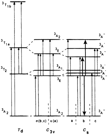 | ||
| Fig. 3 Energy levels of Cr4+ in forsterite, showing the effect of descent in symmetry from Td to C3v and Cs. Electric-dipole transitions and their polarisations are indicated. Heavy arrows indicate the lasing transition and possible b-polarised excited state absorption transitions. (Reproduced with permission from ref. 13.) | ||
It is apparent that the success of this laser is fortuitous, in the sense that it derives its viability from the nature of the Cs distortion at the silicon site. Indeed, although many alternative silicate, aluminate and gallate hosts have been investigated and found to have encouragingly long luminescence lifetimes,14 it is only in forsterite analogues and in yttrium aluminium garnet that laser action has been reported.15
The Cr4+∶forsterite laser can be quite efficient. When a 12 mm × 3 mm × 3 mm crystal is pumped by 3.16 W of absorbed power from a Q-switched Nd∶YAG laser at 1.06 µm, up to 600 mW of tunable infrared light can be obtained at a 1 kHz repetition rate. Slope efficiencies of 32% are possible by careful choice of the pump wavelength and polarisation.11 The output extends over the range 1.18–1.37 µm and can be readily doubled to give average powers up to 60 mW in the range 585–660 nm.
Finally, we notice that these three robust tunable lasers, frequency-doubled where necessary, cover most of the spectrum from 285 to 1370 nm. Only a few short frequency ranges are missing.
Electro-optic materials and holographic storage
Novel non-linear optical materials have attracted widespread attention over the last fifteen years, and their characteristics have been comprehensively reviewed,16–23 but the outcome, measured by practical devices in service, is disappointing. Looking back over this period of development, much of the chemical synthetic effort appears to have been ineffective. In many cases, there has been little attempt to use structure–property relationships as a guide to synthesis, as well as an ignorance of the detailed requirements for practical optical devices.Most non-linear optical devices derive their properties from a change in the refractive index arising from an electronic polarisation induced either by a low frequency electric field, or by optical fields. At low frequencies, in an acentric medium, the dominant component of the index change is linear in the electric field. This electro-optic effect can introduce a phase shift into one arm of a waveguide interferometer, so as to effect amplitude modulation, as well as optical routing and switching—functions that are central to optical communication systems.
Modulation of the index by optical frequency fields leads to second harmonic generation. Initially, it was hoped that compact blue sources might be obtained by frequency doubling red light from well-established and efficient (In/Ga/Al)As diode-lasers. However subsequent advances in blue light-emitting diodes and lasers, based on gallium nitride, have largely displaced this approach.
Electro-optic materials
Much is now known, as a result of synthesis and measurement as well as through theoretical work, about the criteria that must be met for chromophores to exhibit a large electro-optic response.20,24,25 An intense electronic transition should be present in the visible or near UV that carries with it a major change in the molecular dipole moment. Charge-transfer transitions, between groups separated by a long conjugated chain, are thus a natural choice. However, a balance needs to be struck. Strong delocalisation may ensure a large transition moment and an intense transition, but at the expense of a relatively uniform charge distribution in both the ground and the excited states, and thus a relatively small change in dipole moment. Conversely, strong charge localisation will lead to a large change in dipole moment, but also a lower transition intensity as the overlap between the donor and acceptor groups decreases.26The modification of the optical polarisability in an external field originates primarily from the Stark shift of the charge-transfer transition,26 caused by the change in dipole moment in the excited state. In a bulk sample, the extent to which this molecular charge displacement can be aligned parallel to the external field determines the field-induced change in the optical polarisability (i.e. the hyperpolarisability), and thus in the refractive index.
In a few instances, a favourable alignment can be engineered into crystalline
materials, but usually it must be induced artificially in glassy media. In
the polymeric materials that are well suited to the lithographic definition
of waveguides, chromophore alignment is achieved by applying a ‘poling’
electric field above the glass transition temperature Tg.
The alignment is “fixed” by subsequent cooling. For this to be
effective, the molecule must possess a large ground state dipole moment. Molecule 1 is typical of the class of compound that has
emerged after many years of optimisation work in this field.27
It has both a large ground state dipole moment and a large hyperpolarisability.

The durability of the non-linearity depends on how effectively the alignment can be locked into the material, either through the immobility of the polymer chains at low temperature, or by chemically cross-linking them in the poled condition. A common immobilisation strategy links the non-linear chromophore covalently to the polymer backbone via a flexible sidechain. While long-term poling stability can be enhanced by using rigid polymers with a high Tg, the non-linear chromophore may need to be modified to survive at this temperature. Several of the features of 1, such as the incorporation of the donor amine into a piperidine ring, the use of thiophene rings in the conjugating system, and the phenyl substitution of the nitrogen atoms in the thiobarbituric acid acceptor unit, were incorporated for this purpose.27
A critical feature of an electro-optic waveguide is the propagation loss due to absorption. This can be quantified by a figure of merit W, that describes the number of wavelengths of phase shift that are possible in a (1/e) attenuation length, when the electric field is at the limit determined by dielectric breakdown.28,29 Unless W > 2, it will be impossible to construct a useful interferometric device without incurring unacceptable absorption losses. This factor is much more demanding than might be expected from an examination of the absorption spectrum in solution.
At the edge of a Gaussian charge-transfer band, the absorption loss falls off exponentially, while the linear electro-optic coefficient follows the dispersion in the refractive index and scales as (ω02−ω2)−1. A crude calculation shows that, for a chromophore with a large non-linearity, the figure of merit W only reaches an acceptable value on the red side of the band when the optical frequency is displaced by more than twice the full-width half-maximum (FWHM) from the band centre.26 For an intense transition centred at 500 nm and with a FWHM of 5000 cm−1, it is therefore not possible to construct a device operating at shorter wavelengths than 1 µm. On a linear scale, the absorption coefficient in this example appears negligible at 600 nm, and at 1 µm it is ca. 10−6 of that at the band maximum. However, this is still too large to be adequately transparent in the length (ca. 5mm) of device having the necessary electro-optic phase shift.
Recently, it has been shown that most organic non-linear chromophores undergo slow photochemical degradation at infrared wavelengths, although superficially the probability of an electronic excitation in this region appears to be very small.30 The rate at which the chromophore degrades is an exponential function of the displacement from the band centre, and correlates well with absorption in the Gaussian tail. In most cases, the lack of stability is due to oxidation, but it can also be due to isomerisation.
Unfortunately the near IR absorption coefficient, and with it the extent of the photochemical damage, increases by several orders of magnitude in polymer matrices compared to fluid solutions.31 This absorption correlates with the Tg of the matrix. It has been attributed to the inhomogeneous broadening of the charge-transfer transition in the rigidly disordered high-Tg polymers. Chromophores designed to exhibit large Stark shifts in an external field are inevitably sensitive to inhomogeneous perturbations by non-uniformities in the local electric field within a glassy matrix of this type. Unfortunately, the rigidity required to maintain the molecular alignment also has the effect of increasing the extent of near IR absorption and the rate of photodecomposition.
Despite the very small absorption coefficients in the near IR, the consequences
are serious. The rate of loss under irradiation of the active chromophore
in the side-chain polymer 2,
predicts that a waveguide modulator, carrying 1 mW of power at the
1320 nm telecommunications wavelength, will have a (1/e)
lifetime of 12 days.30 An acceptable
service life would be 10 years. Moreover, a survey of the photostability of
eight different chromophores with absorption maxima near 500 nm shows
that their lifetimes are currently one or two orders of magnitude short of
meeting this target.32 It remains to be seen
whether packaging that excludes atmospheric oxidation, will be able to overcome
this obstacle. Photochemical degradation is even more serious in polymeric
waveguide devices intended for second harmonic generation, because the rate
of decomposition increases at the shorter wavelength of the harmonic.33

Photorefractive holographic storage
Fortunately, there are other applications of the electro-optic effect where the photo-stability of the medium is less critical. Holographic memory materials are a particularly important example. Typically, data is recorded in a light sensitive medium in the form of an interference pattern between two mutually coherent beams, one of which (the signal beam) passes through a spatial light modulator (SLM). This component may typically consist of a 1000 × 1000 pixel (i.e. 1 Mbit) array, each element of which can be switched between opaque and transmitting states. The recording material samples the spatial distribution of intensity in the interference pattern, storing it photo-chemically in the form of local changes that are manifest in either the absorption coefficient or the refractive index. This pattern or hologram contains information about the relative phase and amplitude of both beams at the moment of recording. If a replica of the reference beam illuminates the hologram, its diffraction creates an exact copy of the original intensity distribution in the signal beam, thereby allowing recovery of the stored data.There are two great attractions in holographic storage.34 Firstly, the state of a single SLM pixel is spatially encoded in the entire volume of the hologram, so small defects in the medium slightly decrease the overall signal-to-noise ratio, but do not result in loss of data. Secondly, storage is an intrinsically parallel process. If the hologram from a 1 Mbit SLM can be written in 1 ms, the equivalent writing speed is 1 Gbit s−1, while reading speeds are limited only by the rate of acquisition from a photodiode array. Moreover, if the recording material is thick (i.e.ca. 100 µm), the Bragg condition means that a change in the reference beam angle between recording and readout destroys the image reconstruction. It is therefore possible, either by using different angles between the writing beams or different wavelengths, to store a large number of non-interfering holograms simultaneously within the same volume. The potential memory capacity is large—as many as 5000 holograms have been stored in a 6 mm thick lithium niobate crystal.35
The power of this method, however, remains largely unrealised because of limitations in the recording materials. These should have high sensitivities to keep the recording time short and must use reversible photochemistry if a read–write memory is required. The main obstacle, however, is the lack of stability of the hologram during readout. The additional photochemistry that occurs during this period reduces the contrast in the spatial modulation that encodes the data within the material, and thus the definition of all the holograms stored within it.34
One of the most promising classes of materials for holographic storage makes use of the photo-refractive effect. The principle is straightforward. Photo-ionisation of electrons in regions of high intensity causes a redistribution of charge towards traps in regions of low intensity, and thus large spatially modulated local electric fields. Providing the material has a large electro-optic coefficient, these fields will cause spatial modulations in the refractive index.
In classical photorefractive materials, such as iron-doped LiNbO3,
the electro-optic effect is an intrinsic property of the host crystal.
However, it is not easy to grow large stoichiometric single ferroelectric-domain
crystals for use as a general-purpose storage medium.36
Given the low cost and ease of preparation of optically homogeneous polymer
films, a viable alternative is to use the same class of non-linear optic
chromophore that is effective in electro-optic phase modulators. The linear
electro-optic effect is again obtained by orienting polar molecules in
an external electric field above Tg. In a typical example,
the internal electric fields are generated by the addition of a photosensitiser,
2,4,7-trinitro-9-fluorenone 3,
whose strong electron-accepting properties allow it to capture a photo-excited
electron from a hole-transporting conducting polymer, such as poly(N-vinylcarbazole)
4. The electro-optic component is 2,5-dimethyl-4-(p-phenylazo)anisole 5. Such materials can have good long-term
data storage characteristics due to the orientational stability of rigid high-Tg
polymers.37

When a short-term memory is acceptable, a large improvement in sensitivity can be obtained by using a host in which Tg is engineered to be close to ambient temperature by the addition of a plasticiser. In the above example, this can be achieved, without adversely affecting the charge-transport properties, by adding N-ethylcarbazole as a diluent. The polar non-linear optic chromophores can now reorient easily under the combined influence of the externally poling field and the local space-charge field created by the photo-ionisation, resulting in a much enhanced non-linearity.38 In addition, the local birefringence associated with the linear anisotropy of these chromophores enhances the modulation depth for polarised light. Although such materials have improved sensitivity, they currently do not compete with the best inorganic materials.39
Methods for fixing holograms against erasure during readout have not yet been perfected, although a number of schemes have been tried.40 Here, just one promising approach is described. The recording medium is a LiNbO3 crystal doped with both iron and manganese ions.41 As might be expected from the redox potentials, the Mn2+/Mn3+ level lies deeper relative to the conduction band than the Fe2+/Fe3+ level. Fe2+ centres can be ionised by red light, but Mn2+ can only be ionised by UV light—both processes can also be described as M2+ to Nb5+ charge transfers. Initially the material contains Mn2+ and Fe3+, and is transparent in the region where Fe2+ absorbs. It can, however, be made sensitive to red light by exposure to UV, so that the trapping of conduction-band electrons creates a uniform, metastable population of Mn3+ and Fe2+ ions.
If red light is used to write the hologram, ionisation in high intensity regions creates a local increase in the concentration of Fe3+ ions. The electrons are preferentially trapped in darker regions where they reduce Fe3+ to Fe2+ and Mn3+ to Mn2+. If the exposure is continued until all the Fe2+ ions are photo-oxidised, the absorption of red light is bleached. Eventually, lower intensity regions also become bleached and the diffraction efficiency, after passing through a maximum, decreases towards zero.
When the hologram is written with red beams, but at the same time is uniformly illuminated with UV light, electrons ionised from Mn2+ can continually replenish the Fe2+ concentration. The spatially modulated ionisation by red light can therefore continue without bleaching, but in doing so preferentially creates an excess of Mn2+ ions in regions where the intensity is high and the concentration of Fe2+ is low. Eventually the hologram consists of complementary spatial modulations of both the Mn2+ and Fe2+ concentrations. If the UV source is now turned off, red light eventually bleaches the absorption of all the Fe2+ ions, but the space charge pattern remains imprinted in the Mn2+ distribution. The hologram is thus completely involatile (over a period of several days) under interrogation by red light. It can however be erased with UV.
The sensitivity of this material is such that the exposure of 1 mm2 to 10 mW of absorbed red light provides a diffraction efficiency of 10−6 in less than 35 ms, corresponding to a recording rate of ca. 30 Mbits s−1. Given the difficulty of preparing low-cost holographic media in LiNbO3, it will be important to see whether an analogous scheme of dual-trap/dual-wavelength writing can be devised for use in poled polymers.
In a 1 mW readout beam, it is easy to detect holographic diffraction efficiencies of the order of 10−6. Since the efficiency is ca. (πδnd/λ)2, where d is the thickness and δn is the index modulation, a 1 mm thick sample only requires δn ≈ 10−6 to be useful. More generally though, a hologram illustrates how index modulations with periods comparable to an optical wavelength can be used to accurately manipulate a portion of an optical wavefront by diffraction. In the next section, we shall see how much larger amplitude spatial modulations in the material properties can be exploited to gain comprehensive control over optical propagation.
Microstructured photonic devices
Materials patterned with large refractive index contrast have applications in a wide range of photonic devices. The simplest illustrative structures are multilayer dielectric mirrors, also called distributed Bragg reflectors (DBR), usually made from a stack of alternating layers of very different refractive index, such as SiO2 (n ≈ 1.45) and TiO2 (n ≈ 2.7). The thickness of each layer is chosen so that the portion of the wavefront reflected at its interfaces suffers a round-trip phase shift of λ/2. Multiple interference between waves scattered from all the interfaces ensures that the stack has no transmission. Because there is no absorption loss at visible wavelengths in either material, the reflectance is typically >99%, whereas the reflectance of a metallic mirror is ca. 95%. The absence of absorption loss is useful for avoiding mirror damage in high-power laser beams.The wavelength range over which a high reflectance is obtainable increases with the index contrast between the layers. Indeed, a close analogy can be drawn between the solutions to Maxwell's equations for a photon propagating in a medium with a periodically varying dielectric constant, and the solutions to Schrödinger's equation for an electron in periodic potential.42 One-dimensional periodicity leads, in both instances, to bandgaps in the frequency spectrum of propagating waves—the gap width being proportional to the modulation depth of, on the one hand, the dielectric constant or, on the other, the electrostatic potential. Within a photonic bandgap, the optical field is evanescent at the boundaries, and there are no propagating modes.
There are major applications for DBR's in fibre optics, where they are usually called Bragg gratings. They can be made by irradiating a germanium-doped silica fibre core at right angles to the fibre axis, with UV excimer laser pulses near 240 nm. The grating is defined either by means of a mask or by the interference fringes at the conjunction of two beams. Densification of the glass in regions of high intensity introduces a small (ca. 10−4) spatial modulation in the refractive index parallel to the fibre axis.43–45 Consequently, the photonic bandgap is also small and the grating behaves as a very narrow bandwidth reflector. Its reflectance can nevertheless be high because of the large number of grating periods. Mirrors of this kind can provide wavelength-selective feedback in, for example, the erbium-doped fibre lasers that are used in the 1.5 µm telecommunications window. Indeed, a set of Bragg gratings can select many different lasing wavelengths from within the gain bandwidth of the erbium ions. They provide a simple and robust means for the wavelength division multiplexing (WDM) of data in a fibre-optic transmitter, while matching gratings are used at the receiver to de-multiplex the output.
The shift in centre wavelength due to small changes in the effective grating period, is used in a growing array of remote fibre-optical sensors, e.g. for temperature, pressure and strain.46 Because the evanescent part of the optical field extends beyond the surface of the fibre, selective chemical binding on the surface changes the effective grating period. The shift in the reflected wavelength allows it to be used for remote chemical sensing.
Bragg mirrors can be used to define an optical microcavity—a thin planar medium (of refractive index n) bounded by high reflectance mirrors separated by λ/2n. If spontaneous emission occurs within the medium, its directionality, wavelength and lifetime can be modified relative to the same emission in free space.47 This happens because the accessible modes of the radiation field are constrained by the boundary conditions of the cavity. The density of final states in the Fermi golden rule is therefore anisotropic, causing strongly directional emission normal to the mirrors. This feature forms the basis of vertical cavity surface emitting semiconductor lasers (VCSELs), which are of growing importance.
The effect of optical confinement by a microcavity can be seen in the efficiency of second harmonic generation (SHG) in a poled polymer film.48 One mirror of the cavity is a Bragg SiO2–TiO2 stack that is reflective between 980 and 1100 nm, but transparent to the second harmonic radiation near 525 nm. The other mirror is a thin film of silver that is partially transparent to the near-IR pump radiation, as well as being used as an electrode to pole the polymer within the microcavity. The measured SHG efficiency is a very sharp function of the fundamental frequency. When this matches the cavity resonance, the efficiency exceeds that in the absence of the cavity by a factor of 50.
The visible emission of the conjugated polymer poly(p-phenylene-vinylene) (PPV), which is widely used in organic light-emitting diodes, can be enhanced by more than two orders of magnitude in the forward direction by enclosing it in a microcavity bounded by two broadband Bragg mirrors.49 These are designed to have a high reflectance across the whole of the spontaneous emission bandwidth from 500 to 650 nm. The on-axis emission is enhanced by the high finesse of the microcavity. It occurs only in a narrow band defined by the cavity resonance near 550 nm, so light emitted in this direction is virtually monochromatic. Further line narrowing at this wavelength is observed when the pump power is high enough to enable stimulated emission. This demonstration may have important implications for electro-luminescent devices that use polymers of this type, because monochromatic sources improve the chromatic quality in display screens.
The fabrication of microcavities and Bragg mirrors is not easy, so it would be helpful to find simpler ways of coupling light efficiently out of a thin electro-luminescent film. A large proportion (ca. 1/2n2) of the emission from such a film is unusable because it is trapped by total internal reflection and guided to the periphery. The effect is particularly severe in PPV films because of their very high refractive index (n ≈ 2.2); less than 1/8th of the radiation is available externally. A simple solution is to spin coat the emissive layer onto a sublayer of photoresist that has been patterned holographically to create a set of periodic corrugations on both surfaces of the film. When the grating vector matches the propagation vector of a waveguide mode, light is Bragg scattered normal to the surface of the film. Fig. 4 shows the emission in a direction near normal to the surface of a PPV film which has been structured in this way, and illustrates the enhancement at wavelengths satisfying the Bragg condition.50
 | ||
| Fig. 4 PPV emission spectrum approximately normal to a thin film spun on (lower trace) a planar substrate, and (upper trace) a corrugated layer of photoresist. (Reproduced with permission from ref. 50.) | ||
3-Dimensional photonic crystals
Much of the excited state population in a conventional one-dimensional laser cavity is lost through spontaneous emission from the open sides where there is no confinement. No inversion is possible until the pumping rate overcomes this loss. Inevitably, any pump power below this threshold is wasted. It is therefore interesting to ask whether a three-dimensional cavity, based on the principles of the Bragg mirror, can completely suppress these losses. What is required is a material in which the dielectric constant is modulated periodically in three dimensions on a scale comparable to the wavelength of visible light. Such structures have become known as photonic crystals.If the contrast in the dielectric constant is large enough, it should be possible to create a photonic bandgap within which no propagating electromagnetic modes exist. The loss of photons from a cavity would then be prevented in all directions, completely inhibiting spontaneous emission. Yablonovitch was the first to formulate this idea,51 and its ramifications have since been widely explored theoretically. Numerous device principles that exploit this property have been identified.52–56 One important example is the formation of a waveguide, formed by a line of defects, within the photonic crystal lattice.53,55 The complete confinement of the electromagnetic field within the guide ensures that it can propagate around sharp bends with radii comparable to the optical wavelength. The implications for the fabrication of dense highly integrated optical circuitry are clearly far-reaching.
Because there are no well-developed methods for making structures that are periodic in three dimensions on the scale required for visible light, experimental work on 3-D photonic crystals has not kept up with the theory. Established methods of sub-micron fabrication are based on the lithographic patterning of planar substrates—so most experimental structures are periodic only in two dimensions. They are typically made by etching a hexagonal pattern of air holes in a planar waveguide composed of a high refractive index semiconductor, such as GaAs.56 Such structures lose light by diffraction into free space in the region of the air holes, so confinement normal to the plane of the waveguide is incomplete. Nevertheless, several of the expected properties have been confirmed. Notably 1.55 µm radiation, confined in a guide bounded by a hexagonal pattern of air holes in silicon, can be transmitted through a 120° bend with a radius of 0.8 µm.57
3-D periodic structures are more difficult to construct. One heavyweight approach is to form a 2-D periodic structure lithographically in a thin layer of silicon, and to repeat this process, after a suitable planar transformation of the pattern, in subsequent overgrown layers. This technique can only define structural elements with vertical sides, and imposes extreme demands on the lateral registration between layers. It is slow and expensive, and has not produced a crystal more than a few lattice periods deep.58–61
The lattice type of a photonic crystal is important. Complete confinement requires an omni-directional gap. This can be most easily achieved if the Brillouin zone is close to spherical, and the most suitable Bravais lattice in this respect is face-centred cubic.62 FCC structures with appropriate dimensions can be made by the self-assembly of mono-disperse colloidal spheres, usually composed of silica, latex or polystyrene. These are commercially available in a variety of sizes and, in suspension, form colloidal crystal arrays in which the charge on the particles confers the necessary long-range order.63,64 The silica materials are, in effect, artificial opals and all these colloidal crystals share the iridescence of natural opal. Although substantial domains of FCC order can be obtained in this way, it is difficult to exclude stacking faults and dislocations on scales larger than 100 µm.
Band structure calculations suggest that a refractive index contrast of ca. 2.5 is necessary to obtain an omni-directional gap. However, the refractive indices of silica or latex particles are small (ca. 1.4), so crystals formed from these colloidal particles, with air in their interstices, are not useful in themselves. Much larger bandgaps, and a more favourable band-structure, can be obtained by using these crystals as templates for complementary (i.e. negative) structures made by infilling the interstices with high-index material. Once the template has been removed by dissolution or calcining, the structure consists of connected air spheres in a matrix of, for example, TiO2 or CdSe.65 Although promising, crystals of this type have not yet been shown to possess a full photonic bandgap. In addition, it is difficult to maintain crystalline order over a large area and there is almost no freedom in this method either to vary the crystallographic basis or to introduce defects in a controlled fashion.
An alternative approach is to build the structure layer by layer. In principle, this can be done by traversing the tightly focussed spot from a laser equipped with a shutter across the sample so as to create insoluble material by photo-polymerising a precursor. This technique is well established on a larger scale, under the name stereo-lithography, for rapidly forming plastic components of complex shape. The length of the beam-waist normal to the focal plane limits the depth resolution. However, the contrast and definition of small objects can be considerably improved by using two-photon absorption to initiate the photo-polymerisation, because the initiation rate then depends on the square of the intensity. Currently, however, this method has not succeeded in defining features smaller than a few microns in length.66
A very recent alternative makes use of 3-dimensional holographic lithography, to create the required periodic microstructure in a single optical exposure.67 The spatial intensity modulations are obtained by the interference of four non-coplanar laser beams in a ca. 30 µm thick film of photoresist. The intensity distribution in the resulting interference pattern has 3-dimensional translational symmetry, its primitive reciprocal lattice vectors being equal to the differences between the wavevectors of the beams.68 Highly exposed photoresist is rendered insoluble; unexposed areas are dissolved away to reveal a 3-dimensionally periodic structure formed of cross-linked polymer with air-filled voids. The four laser beam wavevectors determine the translational symmetry and lattice constant of the interference pattern. Their intensities and polarisations allow considerable freedom in determining the distribution of dielectric material within the unit cell, which in turn determines the photonic band structure.69,70
When 355 nm radiation is used to define the interference pattern, 24 different beam configurations, defining distinct FCC reciprocal lattices, can be found, with unit cell parameters distributed between 397 to 2000 nm. In each case, the shape of the crystallographic basis can be manipulated by controlling the beam polarisations. This method, therefore, has remarkable structural versatility, without requiring any change in the exposure wavelength or the concomitant changes in photo-resist composition that would be required were this not the case.
Fig. 5 shows a simulation of a constant intensity surface for two such configurations. The first has a = 922 nm, and the second a = 397 nm. Notice the difference in the shape of the primitive basis in each case. Fig. 6 shows the incident beams wavevectors used to form the structure in Fig. 5a. Their differences generate primitive translation vectors in a body-centred cubic reciprocal lattice that corresponds to the FCC lattice in direct space.
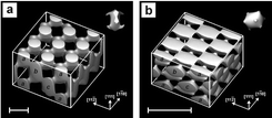 | ||
| Fig. 5 Calculated constant intensity surfaces in four-beam laser interference patterns designed to produce photonic crystals. The primitive basis is shown in each case. (a) FCC pattern with lattice constant 922 nm. The close-packed layers are shown on one side of the cube. (b) FCC pattern with lattice constant 397 nm. Scale bars: 500 nm. (Reproduced with permission from ref. 67.) | ||
 | ||
| Fig. 6 Beam geometry for the FCC interference pattern in Fig. 5a. The wavevectors for the four laser beams are shown in red. Their differences define a set of primitive translations that relate four lattice points (green), constituting a primitive unit cell of the bcc reciprocal lattice (blue). | ||
Fig. 7 shows a scanning electron
micrograph of a polymeric epoxy structure made in this way. The exposure is
made by a single 6 ns laser pulse at 355 nm, after which a 2 min
heat treatment completes the polymerisation. The material is then sonicated
in a solvent for ca. 20 min to develop the structure. Infilling
with Ti(OEt)4, followed by hydrolysis and calcination
at ca. 400°C, leads to the structural complement of the
polymer template formed from TiO2. Several different infilling
methods have been demonstrated, using colloidal crystals as templates for
SiO2, TiO2, ZrO2, Al2O3,
Nb2O5, WO3, CdSe, CdS, Au, Ni, Cu, Ag, and
Pt.65 The scope for fabricating materials
with a wide range of optical properties, based on holographically defined
templates, is therefore substantial. This approach, when developed, may well
offer a rapid, cheap route towards the manufacture of these important photonic
components.
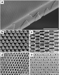 | ||
Fig. 7 SEM images of photonic
crystals generated by holographic lithography. (a) Polymeric crystal
formed by exposure of a 10 µm film of photoresist to the interference
pattern shown in Fig. 5a. The top surface
is a (111) plane; the film has been fractured along the (11![[1 with combining macron]](https://www.rsc.org/images/entities/char_0031_0304.gif) )
cleavage planes. Scale bar 10 µm. (b) Close-up
of a (111) surface. Scale bar: 1 µm. (c)
Close-up of (11) surface. Scale bar: 1 µm. (d)
Inverse replica in TiO2 using the polymeric structure in (a)
as a template. Scale bar: 1 µm. (e)
(02)
surface of a BCC crystal formed using a different beam pattern. Scale bar:
1 µm. (Reproduced with permission from ref. 67.) )
cleavage planes. Scale bar 10 µm. (b) Close-up
of a (111) surface. Scale bar: 1 µm. (c)
Close-up of (11) surface. Scale bar: 1 µm. (d)
Inverse replica in TiO2 using the polymeric structure in (a)
as a template. Scale bar: 1 µm. (e)
(02)
surface of a BCC crystal formed using a different beam pattern. Scale bar:
1 µm. (Reproduced with permission from ref. 67.) | ||
Conclusion
Chemical synthesis continues to be important in refining the electronic structure of optical materials. This is true both in the development of optical sources, as well as in the optimisation of properties that can be modulated as a function of time and which allow the instantaneous control of propagation. However, micro-structured photonic materials promise a future in which photons can be manipulated as readily as electrons and, in due course, all-optical alternatives to electronics. New materials technologies, with the ability to accurately pattern dielectrics and semiconductors in three dimensions on a sub-micron scale, are in urgent need of development for this purpose.References
- G. Blasse and B. C. Grabmaier, Luminescent Materials, Springer-Verlag, Berlin, 1994. Search PubMed.
- R. T. Wegh, H. Donker, K. D. Oskam and A. Meijerink, Science, 1999, 283, 663 CrossRef CAS.
- B. Henderson and G. F. Imbusch, Optical Spectroscopy of Inorganic Solids, Oxford University Press, Oxford, UK, 1989. Search PubMed.
- P. F. Moulton, Proc. IEEE, 1992, 80, 348 CrossRef CAS.
- P. F. Moulton, J. Opt. Soc. Am. B, 1986, 3, 125 Search PubMed.
- M. G. Kovalsky, A. A. Hnilo and C. Inchauspe, Opt. Lett., 1999, 24, 1638 Search PubMed.
- M. J. Bohn, R. J. Jones and J. C. Diels, Opt. Commun., 1999, 170, 85 CrossRef CAS.
- C. D. Marshall, J. A. Speth, S. A. Payne, W. F. Krupke, G. J. Quarles, V. Castillo and B. H. T. Chai, J. Opt. Soc. Am. B, 1994, 11, 2054 Search PubMed.
- K. I. Schaffers and D. A. Keszler, Acta Crystallogr., Sect. C, 1991, 47, 18 CrossRef.
- A. J. S. McGonigle, D. W. Coutts and C. E. Webb, Opt. Lett., 1999, 24, 232 Search PubMed.
- N. V. Kuleshov, A. V. Podlipensky, V. G. Shcherbitsky, A. A. Lagatsky and V. P. Mikhailov, Opt. Lett., 1998, 23, 1028 Search PubMed.
- D. J. Robbins and A. J. Thomson, Mol. Phys., 1973, 25, 1103 CAS.
- N. V. Kuleshov, V. G. Shcherbitsky, V. P. Mikhailov, S. Hartung, T. Danger, S. Kuck, K. Petermann and G. Huber, J. Lumin., 1997, 75, 319 CrossRef CAS.
- C. Anino, J. Thery and D. Vivien, Opt. Mater., 1997, 8, 121 CrossRef CAS.
- K. A. Soubbotin, V. A. Smirnov, S. V. Kovaliov, H. J. Scheel and E. V. Zharikov, Opt. Mater., 2000, 13, 405 CrossRef CAS.
- D. R. Kanis, M. A. Ratner and T. J. Marks, Chem. Rev., 1994, 94, 195 CrossRef CAS.
- D. M. Burland, Chem. Rev., 1994, 94, 1 CrossRef.
- D. P. Shelton and J. E. Rice, Chem. Rev., 1994, 94, 3 CrossRef CAS.
- D. M. Burland, R. D. Miller and C. A. Walsh, Chem. Rev., 1994, 94, 31 CrossRef CAS.
- J. Zyss and I. Ledoux, Chem. Rev., 1994, 94, 77 CrossRef CAS.
- R. M. Corn and D. A. Higgins, Chem. Rev., 1994, 94, 107 CrossRef CAS.
- W. E. Moerner and S. M. Silence, Chem. Rev., 1994, 94, 127 CrossRef CAS.
- J. L. Bredas, C. Adant, P. Tackx, A. Persoons and B. M. Pierce, Chem. Rev., 1994, 94, 243 CrossRef CAS.
- S. R. Marder, D. N. Beratan and L. T. Cheng, Science, 1991, 252, 103 CrossRef CAS.
- D. J. Williams, Nonlinear Optical Properties of Guest–Host Polymer Structures, in Non-linear Optical Properties if Organic Molecules and Crystals, Part I, ed. D. S. Chemla and J. Zyss, Academic Press, Inc., London, 1987. Search PubMed.
- R. G. Denning, J. Mater. Chem., 1995, 5, 365 RSC.
- S. Gilmour, R. A. Montgomery, S. R. Marder, L.-T. Cheng, A. K.-Y. Jen, Y. Cai, J. W. Perry and L. R. Dalton, Chem. Mater., 1994, 6, 1603 CrossRef CAS.
- V. Mizrahi, K. W. DeLong, G. I. Stegeman, M. A. Saifi and M. J. Andrejco, Opt. Lett., 1989, 14, 1140 Search PubMed.
- G. I. Stegeman, C. T. Seaton, A. C. Walker, C. N. Ironside and T. J. Cullen, Opt. Commun., 1987, 61, 277 CrossRef CAS.
- A. Galvan-Gonzalez, M. Canva, G. I. Stegeman, R. Twieg, T. C. Kowalczyk and H. S. Lackritz, Opt. Lett., 1999, 24, 1741 Search PubMed.
- A. C. Le Duff, V. Ricci, T. Pliska, M. Canva, G. I. Stegeman, K. P. Chan and R. Twieg, Appl. Opt., 2000, 39, 947 Search PubMed.
- A. Galvan-Gonzalez, M. Canva, G. I. Stegeman, R. Twieg, K. P. Chan, T. C. Kowalczyk, X. Q. Zhang, H. S. Lackritz, S. Marder and S. Thayumanavan, Opt. Lett., 2000, 25, 332 Search PubMed.
- T. H. Dai, K. D. Singer, R. J. Twieg and T. C. Kowalczyk, J. Opt. Soc. Am. B, 2000, 17, 412 Search PubMed.
- G. T. Sincerbox, Opt. Mater., 1995, 4, 370 CrossRef.
- F. H. Mok, Opt. Lett., 1993, 18, 915 Search PubMed.
- K. Kitamura, Y. Furukawa and N. Iyi, Ferroelectrics, 1997, 202, 21 Search PubMed.
- S. R. Marder, B. Kippelen, A. K. Y. Jen and N. Peyghambarian, Nature, 1997, 388, 845 CrossRef CAS.
- W. E. Moerner, S. M. Silence, F. Hache and G. C. Bjorklund, J. Opt. Soc. Am. B, 1994, 11, 320 Search PubMed.
- B. Kippelen, K. Meerholz, Sandalphon, B. Volodin and N. Peyghambarian, Opt. Mater., 1995, 4, 354 CrossRef CAS.
- D. Lande, S. S. Orlov, A. Akella, L. Hesselink and R. R. Neurgaonkar, Opt. Lett., 1997, 22, 1722 Search PubMed.
- K. Buse, A. Adibi and D. Psaltis, Nature, 1998, 393, 665 CrossRef CAS.
- P. S. J. Russell, T. A. Birks and F. D. Lloyd-Lucas, in Photonic Bloch Waves and Photonic Band Gaps, ed. E. Burstein and C. Weisbuch, Plenum Press, New York, 1995. Search PubMed.
- P. Niay, M. Douay, P. Bernage, W. X. Xie, B. Leconte, D. Ramecourt, E. Delevaque, J. F. Bayon, H. Poignant and B. Poumellec, Opt. Mater., 1999, 11, 115 CrossRef CAS.
- M. Douay, W. X. Xie, T. Taunay, P. Bernage, P. Niay, P. Cordier, B. Poumellec, L. Dong, J. F. Bayon, H. Poignant and E. Delevaque, J. Lightwave Technol., 1997, 15, 1329 CrossRef CAS.
- B. Poumellec, P. Guenot, I. Riant, P. Sansonetti, P. Niay, P. Bernage and J. F. Bayon, Opt. Mater., 1995, 4, 441 CrossRef CAS.
- M. W. Hathaway, N. E. Fisher, D. J. Webb, C. N. Pannell, D. A. Jackson, L. R. Gavrilov, J. W. Hand, L. Zhang and I. Bennion, Opt. Commun., 1999, 171, 225 CrossRef CAS.
- H. Yokoyama, Science, 1992, 256, 66.
- H. Cao, D. B. Hall, J. M. Torkelson and C. Q. Cao, Appl. Phys. Lett., 2000, 76, 538 CrossRef CAS.
- S. E. Burns, G. Denton, N. Tessler, M. A. Stevens, F. Cacialli and R. H. Friend, Opt. Mater., 1998, 9, 18 CrossRef CAS.
- B. J. Matterson, M. G. Salt, W. L. Barnes and I. D. W. Samuel, Synth. Met., 1999, 101, 250 CrossRef CAS.
- E. Yablonovitch, Phys. Rev. Lett., 1987, 58, 2059 CrossRef CAS.
- E. Yablonovitch, T. J. Gmitter, R. D. Meade, A. M. Rappe, K. D. Brommer and J. D. Joannopoulos, Phys. Rev. Lett., 1991, 67, 3380 CrossRef CAS.
- J. D. Joannopoulos, P. R. Villeneuve and S. H. Fan, Nature, 1997, 386, 143 CrossRef.
- J. S. Foresi, P. R. Villeneuve, J. Ferrera, E. R. Thoen, G. Steinmeyer, S. Fan, J. D. Joannopoulos, L. C. Kimerling, H. I. Smith and E. P. Ippen, Nature, 1997, 390, 143 CrossRef CAS.
- S. Y. Lin, E. Chow, V. Hietala, P. R. Villeneuve and J. D. Joannopoulos, Science, 1998, 282, 274 CrossRef CAS.
- T. F. Krauss and R. M. De la Rue, Prog. Quantum Electron., 1999, 23, 51 CrossRef CAS.
- M. Tokushima, H. Kosaka, A. Tomita and H. Yamada, Appl. Phys. Lett., 2000, 76, 952 CrossRef CAS.
- S. Y. Lin and J. G. Fleming, J. Lightwave Technol., 1999, 17, 1944 CrossRef CAS.
- N. Yamamoto, S. Noda and A. Sasaki, Jpn. J. Appl. Phys. 1, 1997, 36, 1907 Search PubMed.
- C. C. Cheng, A. Scherer, R. C. Tyan, Y. Fainman, G. Witzgall and E. Yablonovitch, J. Vac. Sci. Technol., B, 1997, 15, 2764 CrossRef CAS.
- J. G. Fleming and S. Y. Lin, Opt. Lett., 1999, 24, 49 Search PubMed.
- E. Yablonovitch and T. J. Gmitter, Phys. Rev. Lett., 1989, 63, 1950 CrossRef CAS.
- J. Wijnhoven and W. L. Vos, Science, 1998, 281, 802 CrossRef CAS.
- S. A. Asher, J. Holtz, L. Liu and Z. J. Wu, J. Am. Chem. Soc., 1994, 116, 4997 CrossRef CAS.
- O. D. Velev and E. W. Kaler, Adv. Mater., 2000, 12, 531 CrossRef CAS.
- B. H. Cumpston, S. P. Ananthavel, S. Barlow, D. L. Dyer, J. E. Ehrlich, L. L. Erskine, A. A. Heikal, S. M. Kuebler, I. Y. S. Lee, D. McCord-Maughon, J. Q. Qin, H. Rockel, M. Rumi, X. L. Wu, S. R. Marder and J. W. Perry, Nature, 1999, 398, 51 CrossRef CAS.
- M. Campbell, D. N. Sharp, M. T. Harrison, R. G. Denning and A. J. Turberfield, Nature, 2000, 404, 53 CrossRef CAS.
- G. Grynberg, B. Lounis, P. Verkerk, J. Y. Courtois and C. Salomon, Phys. Rev. Lett., 1993, 70, 2249 CrossRef CAS.
- K. M. Ho, C. T. Chan and C. M. Soukoulis, Phys. Rev. Lett., 1990, 65, 3152 CrossRef CAS.
- E. Yablonovitch, T. J. Gmitter and K. M. Leung, Phys. Rev. Lett., 1991, 67, 2295 CrossRef CAS.
Footnote |
| † Basis of a presentation given at Materials Discussion No. 3, 26–29 September, 2000, University of Cambridge, UK. |
| This journal is © The Royal Society of Chemistry 2001 |