The electrical characteristics of a heterojunction diode formed from an aniline oligomer LB-deposited onto poly(3-methylthiophene)†
Antonio Riul Jr., Christopher A. Mills and D. Martin Taylor*
Institute of Molecular and Biomolecular Electronics, University of Wales, Dean Street, Bangor, Gwynedd, UK LL57 1UT. E-mail: martin@sees.bangor.ac.uk
First published on UnassignedUnassigned22nd December 1999
Abstract
Organic heterojunction diodes have been formed by depositing a Langmuir–Blodgett (LB) multilayer of 16-mer polyaniline and stearic acid (1∶1) onto films of poly(3-methylthiophene) electropolymerised onto gold electrodes. The diode was completed by depositing small, circular gold counterelectrodes onto the LB film. The devices thus formed show weak rectification. In forward bias it is argued that all the applied field appears across the LB layer. At high applied fields the resulting current follows the Richardson–Schottky equation indicative of electrode limitation, though it is not clear whether the rate limiting step is electron emission from the gold electrode or hole emission from the polymer into the LB film. In reverse bias it is argued that part of the applied voltage appears across the depletion region formed at the interface between the polymer and the LB film resulting in a smaller reverse current for a given applied voltage. The frequency dependence of capacitance and loss for the diode structure is reminiscent of a Maxwell–Wagner dispersion normally associated with a two-layer structure. However, reasonable agreement between experimental data and theoretical modelling is only possible if a third layer, i.e. the depletion region at the interface of the two organic films, is included in the model. This is confirmed by the reverse-bias capacitance–voltage curve which suggests that the device behaves as a Metal–Insulator–Semiconductor (MIS) structure driven into depletion/inversion. In forward bias, when the LB/polymer interface is in accumulation, the capacitance again decreases as the bias voltage increases. While this effect could be ascribed to the presence of a second depletion layer in the device, it is argued that this behaviour arises from the increase in conductance of the LB multilayer shunting the LB layer capacitance.
1 Introduction
Thiophenes and polyanilines are two important classes of conducting polymers owing to their stability in the neutral state. As such they have been investigated for a range of electronic applications. For example, Schottky diodes exhibiting high rectification ratios have been fabricated from electropolymerized poly(3-methylthiophene) (P3MeT) over the last ten years using aluminium or molybdenum as the rectifying contact.1–8 The currents flowing through these devices were found to be sensitive to both the thickness and the doping concentration in the P3MeT film, while thermal annealing was found to improve the rectification ratio.1,3 The electrical characteristics were strongly affected by the exposure of P3MeT film to oxygen and water vapour which changed drastically the rectification ratio of the diodes1,8 presumably by changing the concentration of electronegative dopants in the polymer. At high forward bias, conduction through the devices appeared to be determined by a space-charge-limited-current (SCLC) regime involving an exponential distribution of traps.8 Some evidence has also been given5 for the presence of minority carriers in this normally p-type material.Schottky barriers have been fabricated from polyaniline (PANi) using electropolymerization,9,10 solvent casting11–13 and Langmuir–Blodgett (LB) deposition,14 vacuum deposited films15 and pellets16 of the organic layer. Acid doping of the polyaniline in these devices led to an increase in the rectification ratio, a decrease in the barrier height and a decrease in the width of the depletion region.12,13
Pani has also been successfully employed as an intermediate layer between ITO and MEH-PPV in light emitting diodes (LEDs), improving device performance through better hole injection from the ITO.17–19 Such an effect was also reported20 for insulating cadmium stearate films LB-deposited onto gallium phosphide where an enhanced electroluminescence was tentatively ascribed to increased hole injection from the metal electrode but could also have arisen from the formation of localised defects in the insulating layer at the high device currents employed.
Heterojunctions formed between organic semiconducting materials of different bandgaps offer the possibility of developing device structures with unique electrical properties. P3MeT and PANi with bandgaps of 2.0 eV7 and 3.14 eV15 respectively are potential candidates for forming such junctions. The present paper reports some recent results obtained during an on-going investigation of an organic heterojunction prepared by the LB deposition of a mixed stearic acid–PANi oligomer (16-mer) (1∶1 wt/wt) onto P3MeT films prepared by electrodeposition onto gold substrates. Using the LB technique to deposit the 2nd layer gives the possibility of interposing an ultrathin layer of controlled thickness and composition between the polymer and the counterelectrode. Since the LB layer is expected to be relatively insulating (the 16-mer is undoped) the structure acts essentially as a Metal–Insulator–Semiconductor (MIS) diode, thus enabling a systematic study of the effects of an interfacial layer on charge injection from electrodes into the polymer. As a result, a range of techniques well-known in the study of inorganic interfaces becomes available for investigating the electronic properties of the polymer.
The present experiments differ from those on bilayer polymer films described by Murray and co-workers in the 1980s21–24 in that the latter were carried out in electrolytic solutions to monitor redox activity in polymer films containing redox active species. Such interactions are not expected in the present work, since our measurements were carried out on ‘dry' films so that solid state charge transport processes are expected to be more relevant.
2 Experimental procedures
All devices were prepared in a class 10![[thin space (1/6-em)]](https://www.rsc.org/images/entities/char_2009.gif) 000 clean room. Microscope slides were cleaned with DECON90 and chromic acid, followed by a thorough rinse with ultrapure water (Millipore SuperQ System). A gold film ∼30 nm thick was vacuum evaporated, in a Balzers (TSH 170) turbosystem at pressures less than 10−6 Torr, onto the slides which had been precoated with a thin chrome layer to aid adhesion. Substrates free of visual defects were then selected for the deposition of P3MeT.
000 clean room. Microscope slides were cleaned with DECON90 and chromic acid, followed by a thorough rinse with ultrapure water (Millipore SuperQ System). A gold film ∼30 nm thick was vacuum evaporated, in a Balzers (TSH 170) turbosystem at pressures less than 10−6 Torr, onto the slides which had been precoated with a thin chrome layer to aid adhesion. Substrates free of visual defects were then selected for the deposition of P3MeT.Electrodeposition was carried out in a conventional three-electrode cell connected to a Princeton EG&G, model 273, potentiostat/galvanostat following techniques which have been shown by Taylor and Gomes to result in the growth of films of reproducible thickness and morphology.4 Briefly, a rectangular sheet of platinum foil 2.5 cm × 3 cm acted as the counterelectrode and a clean silver wire as the quasi-reference electrode. One of the gold-coated glass slides, dipped to a depth of 2.5 cm into the electrolyte solution, formed the working electrode. Electropolymerization was effected by anodic oxidation at room temperature in a 0.05 M solution of 3-methylthiophene monomer (Aldrich) dissolved in propylene carbonate (HPLC grade) using 0.1 M of tetrabutylammonium tetrafluoroborate (TBATFB) as the supporting salt. Nitrogen was bubbled through the solution for at least 20 minutes prior to starting the electrodeposition. The nitrogen flux was moderate to avoid both solvent and monomer evaporation. The P3MeT was grown by applying a 2.3 V (vs. Ag) pulse to the working electrode for 3 s after which the potential was reduced to 1.8 V (vs. Ag) and maintained constant until a film of the desired thickness had been grown. Under these experimental conditions, the film grows uniformly over the central area of the working electrode (∼1 cm2) at a rate of about 0.6 µm min−1.25 The films were electrochemically dedoped by reducing the potential of the working electrode to 0.0 V (vs. Ag) until the current had decreased to ∼2.4 µA cm−2. Afterwards, the films were washed with acetone (Aldrich) to remove residual electrolytic solution and dried in a stream of dry-nitrogen.
The monodisperse 16-mer PANi used in this work was synthesised chemically from the tetramer in the leucoemeraldine oxidation state following the procedures of Zhang et al.26 A sample of the 16-mer PANi was mixed with camphorsulfonic acid, dissolved in m-cresol and added to a solution of stearic acid dissolved in chloroform (HPLC) to form a 1∶1 (wt/wt) PANi–stearic acid spreading solution. Earlier work27 had established that films of this composition were stable at the air–water interface and deposited with good deposition ratio. Mixed LB films of the 16-mer PANi and stearic acid were deposited onto the P3MeT films following procedures fully reported elsewhere.27 Briefly, an aliquot of the final solution was spread over the surface of a pure water subphase and 5 min allowed for solvent evaporation before the monolayer was compressed to 25 mN m−1. The P3MeT-coated slides were dipped vertically through the monolayer at a rate of 2 mm min−1. Deposition occurred on both the up- and down-stroke with deposition ratios close to unity. To aid later comparisons, the LB films were deposited in staircase fashion so that three different thicknesses, namely 5, 15 and 41 monolayers, of the 16-mer PANi were accommodated on the same P3MeT layer. The diodes were completed by placing the films in the turbopumped vacuum chamber and evaporating circular gold or aluminium counterelectrodes, 0.8 mm2 in area, onto the free surface of the 16-mer PANi. Electrical connections to the metal electrodes were made using fine gold wire and silver dag.
The electrical characteristics of the diodes were measured both under vacuum (0.12 mbar) and in ambient atmosphere using a HP 4041B pA meter/DC source. The AC characteristics were measured over the range 20 Hz to 1 MHz using an HP 4284A Precision LCR meter. In both cases, the data were logged automatically by computer.
3 Results
The morphology of the electropolymerised P3MeT film was similar to that reported by Taylor and Gomes4i.e. the 0.3 µm films were dense with a nodular structure as seen in the AFM micrographs in Fig. 1. Even in the worst case, the rms roughness over a 25 × 25 µm2 area was less than 24 nm. At higher magnification, the films appeared much smoother with an rms roughness of ∼15 nm over a 0.5 × 0.5 µm2 area. | ||
| Fig. 1 AFM micrographs showing the morphology of a typical P3MeT film ∼0.3 µm thick at different magnifications: (a) 25 × 25 µm; (b) 0.5 × 0.5 µm. In both cases the z-scale is 1 µm per division. | ||
3.1 DC characteristics
Fig. 2 shows the dependence of current density, J, on applied voltage for diodes with LB films of three different thicknesses, (a) 5, (b) 15 and (c) 41 monolayers, deposited onto the same P3MeT layer and furnished with gold counterelectrodes.The diodes exhibit a weak rectification with the higher currents (forward bias) corresponding to hole injection from the lower gold electrode into the P3MeT layer. For both polarities, the device current increased superlinearly with increasing applied voltage. Except for a small difference in reverse bias, it was immaterial whether the device characteristics were measured in air or under vacuum.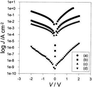 | ||
| Fig. 2 Log Jvs.V for Au/P3MeT/16-mer/Au heterojunctions in air for diodes incorporating (a) 5, (b) 15 and (c) 41 monolayers of LB deposited films of PANi–stearic acid. Curve (d) is for a Au/P3MeT/16mer/Al diode incorporating a 15-monolayer LB film. | ||
Curve (d) in Fig. 2 was obtained for a diode incorporating a 15-layer LB film but furnished with an aluminium counterelectrode. Again the device displays a weak rectification but the striking features is that the currents for both polarities of applied voltage are ∼4 orders of magnitude smaller than for the diode with the gold counterelectrode.
For both polarities of applied voltage in the absence of the LB layers, device currents measured in air with a gold counterelectrode were orders of magnitude greater than the currents reported in Fig. 2. Under vacuum, currents measured in these ‘pure' P3MeT diodes were much reduced owing to a reduced degree of oxygen doping of the P3MeT1 but still remained significantly greater than those reported in Fig. 2 for the heterojunction devices.
3.2 AC characteristics
Fig. 3 shows the experimentally-measured dependence of the diode capacitance and loss on frequency. The capacitance (curve (o)) displays a strong dispersion between 103 and 105 Hz. The corresponding maximum in the AC loss curve (*) is apparently swamped by the presence of a low-frequency loss that rises rapidly as the frequency decreases. | ||
| Fig. 3 Experimentally measured capacitance (o) and loss (*) as a function of frequency for a diode incorporating a 15-monolayer LB film and a gold counterelectrode. The theoretical response (—) of the three element RC equivalent circuit in Fig. 8 for which it is assumed that R1 = 50 Ω, R2 = 1.6 kΩ, Rd = 3.8 kΩ, C1 = 0.2 nF, C2 = 2.0 nF and Cd = 20 nF. | ||
Fig. 4 gives the dependence of device capacitance on applied voltage. Interestingly and unexpectedly, the capacitance is a maximum at zero applied bias and decreases for increasing bias in both forward and reverse directions. For reverse bias (−V), however, the capacitance eventually tends to a constant value at the highest applied voltage but decreases throughout the measurement range with increasing forward bias.
 | ||
| Fig. 4 Capacitance–voltage (C–V) plot for a diode incorporating a 15-monolayer LB film and furnished with a gold counterelectrode. The dotted curve is a theoretical plot based on eqn. (11) for which it has been assumed that CLB = 3.6 × 10⁻⁷ F cm−2, ε = 5 and NA = 1.1 × 1018 cm−3. | ||
4 Discussion
It is well-known that a gold electrode is a good hole injector into P3MeT.4 Furthermore, as indicated above, the forward bias current is significantly reduced in the heterojunction diodes compared with Au/P3MeT/Au diodes for the same magnitudes of applied voltage. Clearly, then, transport through the LB layers appears to be the rate limiting step. That device characteristics were almost independent of whether the measurements were carried out in ambient air or under vacuum provides further confirmation for the controlling influence of the LB layer. In forward bias, polarisation of the P3MeT film will occur with holes accumulating at the P3MeT/LB film interface causing the field in the polymer to collapse. Thus, to a first approximation at least, all the applied voltage may be assumed to appear across the LB layer.Replotting the data in Fig. 2 for the device with gold counterelectrodes in order to show the explicit dependence of device currents on the applied field, E, appearing in the LB layers yields the characteristics in Fig. 5. (The field E is calculated assuming the LB layer to have a thickness of 25 nm per monolayer).28 In forward bias (Fig. 5(a)) the currents appear to follow a square-law dependence on field at high fields suggesting space-charge limitation. In such a regime it is expected that29eqn. (1) holds,
 | (1) |
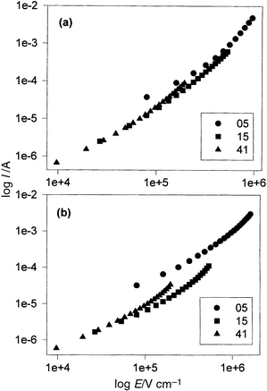 | ||
| Fig. 5 Log Ivs. log E for Au/P3MeT/16-mer/Au diodes with 5, 15 and 41 LB monolayers in (a) forward and (b) reverse bias. The fields were calculated by assuming that all the applied voltage appears across the PANi LB layer. | ||
When the electrode emission is controlled by thermal emission over a field-lowered, image-law barrier, so-called Schottky emission, the dependence of current on applied field is given by the Richardson–Schottky equation29 generally written as the high field approximation eqn. (2),
 | (2) |
 | (3) |
In Fig. 6 the data from Fig. 2 are replotted to test for Schottky emission. As can be seen, for forward bias (Fig. 6(a)) all three curves asymptote to the same linear dependence at the highest fields. That the forward characteristics at high fields are independent of the LB layer thickness is good evidence for the integrity of the LB layers and, more importantly, supports the notion of an electrode limited process. From the gradient at high fields and assuming T = 300 K, βS is estimated to be 1.8×10⁻⁵ (V m)−1/2 from which it is deduced that ε∞ = 4.5 for the mixed stearic acid–16-mer layer. In total some 40 devices on seven different P3MeT films were studied. While some differences were observed in the actual magnitude of the currents flowing at a particular applied field, the functional relationship was identical with values estimated for ε∞ falling in a narrow range from 2.6 to 4.5. This compares with values of 2.71, the reported relative permittivity of stearic acid,30 and 5.6 when the LB layer was formed from the pure 16-mer polyaniline.
 | ||
| Fig. 6 The data in Fig. 5 replotted as log Ivs.E1/2 to test for Schottky emission in (a) forward bias and (b) reverse bias. | ||
The general behaviour seen in Fig. 6(a) coupled with the eminently reasonable range of values estimated for ε∞ provides strong evidence for Schottky emission. This begs the question as to whether the current is an electron emission from the gold counterelectrode or hole emission from the P3MeT into the LB film. Aluminium has a smaller workfunction than gold, and so should favour electron emission. However, from Fig. 2 it is seen that an aluminium counterelectrode reduces both the forward and reverse currents by several orders of magnitude. While this may be taken as evidence against electron emission occurring from the gold counterelectrode, it is known that aluminium forms a Schottky barrier to PANi11,15 and may also have an associated, highly insulating interfacial layer. Therefore no definitive conclusion as to the origin of the barrier to thermal emission in the diode is possible without carrying out further investigations.
In reverse bias the situation is even less clear. At low fields the currents are ohmic but quickly become superlinear as the applied field increases (Fig. 5(b)). Some dependence on the thickness of the LB layer is seen but not that expected from eqn. (1). In any case, since the reverse currents are lower than for forward bias then, de facto, the former cannot be space-charge-limited, unless a different carrier of lower mobility now dominates charge transport. When replotted in Fig. 6(b) a good linear dependence indicating Schottky emission is again seen but in contrast with forward bias βS now depends on the thickness of the LB layer so that values calculated for ε∞ range from 1.8 to 11.
It is notable that, for both forward and reverse bias applied to the device with the thinnest LB layer, extrapolating the I–V plots suggests that the currents flowing at low fields would be greater than expected if low-field transport was dominated by ohmic conduction through the film. If indeed, as suggested, an image-law barrier dominates transport, then it is not surprising that the five-layer film behaves differently to the others. This layer will be sufficiently thin (∼12.5 nm) to cause an overlap of the image law barriers from both interfaces so that even with zero applied field the barrier height is reduced by an amount Δϕb = 2(q2/16πεε0x02) where 2x0 is the thickness of the LB layer. Assuming ε = 4.5 and a film thickness of 12.5 nm, then Δϕb = 0.013 eV, which is sufficient to increase thermal emission currents by a factor 3 or so above that expected in a wider barrier at the same applied field. At high fields, the maximum in the potential barrier moves close to one electrode so that the influence of the second electrode becomes negligible and the dependence on film thickness is lost.
With fields approaching 1 MV cm−1 in a thin barrier, tunnelling may also become a possibility. Parker31 has shown that the DC characteristics of thin PPV films follow the Fowler–Nordheim law,29eqn. (4),
 | (4) |
 | ||
| Fig. 7 The data from Fig. 5(a) replotted as ln I/E2vs. 1/E. | ||
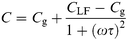
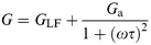
The dispersion in capacitance observed in Fig. 3 appears to follow the behaviour expected from a capacitor composed of two homogeneous layers. The equivalent circuit of such an arrangement is the series-parallel RC circuit shown in Fig. 8(a) where C1 and R1 represent the properties of the P3MeT layer while C2 and R2 represent the stearic acid–16-mer layer. It is readily shown that the admittance of such a circuit is given by4eqn. (5),
 | (5) |
 | (6a) |
 | (6b) |
 | (7) |
 | (8) |
 | (9) |
 | (10) |
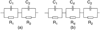 | ||
| Fig. 8 (a) Equivalent circuit of a diode structure composed of two homogeneous layers. R1 and C1 represent the P3MeT layer while R2 and C2 represent the LB deposited 16-mer PANi film. In (b) an additional element Rd/Cd has been included to represent the presence of a depletion region at the interface between the two layers. | ||
In reverse bias, positive voltage applied to the gold counterelectrode, holes are repelled from the P3MeT/LB layer interface creating a depletion region in the P3MeT composed of negatively charged acceptor ions. Consequently, an additional parallel RC element, Rd/Cd must be introduced into the equivalent circuit to represent the depletion region (see Fig. 8(b)). Upon increasing the reverse bias, the depletion region grows while the associated capacitance Cd and hence the overall device capacitance falls33 in a manner described by eqn. (11),
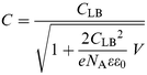 | (11) |
In conventional inorganic MIS devices, when a threshold voltage is reached the semiconductor surface inverts, at which point the device capacitance attains a constant value, a trend seen in Fig. 4. Depletion/inversion at the P3MeT/LB film interface could explain the poor fit of the reverse bias characteristics to the Richardson–Schottky equation. Part of the applied bias will now appear across the depletion region thus reducing the field across the LB layer and hence the current flowing through the device at a given applied voltage.
Assuming now that a depletion region is present at the P3MeT/LB film interface and that the equivalent circuit in Fig. 8(b) applies, a further attempt was made to fit the experimental data in Fig. 3. The results shown by the continuous curves in Fig. 3 were obtained using the parameter set given in the caption and show reasonable agreement with experiment albeit with the latter displaying a wider frequency dispersion than the former. Although this is a 6 parameter fit, the need to reproduce both the capacitance and loss curves simultaneously places severe restrictions on the values that may be adopted for each parameter in the set, otherwise the quality of the fit deteriorates rapidly. Thus each parameter may be deduced within tightly defined ranges.
The theoretical fitting indicates that there are two main dispersions in the system, one in the range 103 to 104 Hz which coincides with that seen in Fig. 3 and the other at 109 Hz which is inaccessible using the present equipment. The low-frequency capacitance is determined in the main by the depletion region capacitance Cd but will depend to some extent on the values of the other components in the circuit. As the signal frequency increases a dispersion occurs with the measured capacitance decreasing to a value determined mainly by the capacitance of the LB layer but again influenced by the relative magnitudes of the other components. Finally at frequencies exceeding those used here a further decrease in capacitance would be expected to a value corresponding to the capacitance of the bulk P3MeT.
From the fit in Fig. 3, the depletion capacitance is deduced to be 20 nF and assuming that ε ∼5 for P3MeT the width of the depletion region, dd (= εε0A/Cd), is estimated to be ∼1.8 nm. This is orders of magnitude lower than the thickness of ∼300 nm measured for the bulk P3MeT layer using the AFM and a value of ∼180 nm deduced from C1 = 0.2 nF used to obtain the best fit in Fig. 3. The best fit value for the capacitance of the 15-layer LB films, C2 = 2.0 nF, yields a low-frequency relative permittivity of ∼10.6 which is approximately twice the high-frequency relative permittivity deduced from the Schottky plots in Fig. 6.
Returning now to Fig. 4, in forward bias the decrease in capacitance with voltage is readily explained by the ‘lossy' nature of the LB layer. In this polarity, the depletion region at the interface is replaced by an accumulation layer, and the device equivalent circuit reverts to that in Fig. 8(a). As the bias increases, the LB-layer becomes more conductive, R2 decreases and begins to shunt C2, the capacitance of the LB layer, so that the measured capacitance will tend to C1, the capacitance of the P3MeT layer.
5 Conclusions
A heterojunction diode has been formed by the controlled LB deposition of a 1∶1 (wt/wt) mixture of stearic acid and 16-mer polyaniline onto electropolymerised P3MeT. Although the dependence of capacitance on voltage indicates the presence of a depletion region in the structure and rectification, albeit weak, is observed, the diodes are examples of MIS devices, in which most of the applied voltage appears across the LB layer.The I–V characteristics in forward bias follow closely the Richardson–Schottky equation yielding a high-frequency relative permittivity in the range 2.6–4.5 for the LB-deposited layer. There is insufficient evidence to determine whether the current is an electron emission from the gold electrode or a hole emission from the P3MeT into the LB film. In reverse bias, Schottky emission is again believed to be the dominant conduction mechanism. However, agreement with theory is not as good, probably because part of the applied potential appears across the depletion/inversion layer present on the P3MeT side of the heterojunction.
At first sight, the AC characteristics appear to follow the simple Maxwell–Wagner model for a two-layer capacitor. However, only when a third RC element representing the depletion region is added to the equivalent circuit is it possible to obtain good agreement between theory and experiment.
In reverse bias the capacitance–voltage plot exhibits the behaviour of a classic MIS structure from which the doping density in the P3MeT is estimated to be 1.1 × 1018 cm−3.
Acknowledgements
The authors are pleased to acknowledge the financial support provided by the Engineering and Physical Sciences Research Council and BNFL (CASE studentship to CAM) and are grateful to FAPESP for the award of the Research Fellowship to AR.References
- D. M. Taylor, H. L. Gomes, A. E. Underhill, S. Edge and P. I. Clemenson, J. Phys. D: Appl. Phys., 1991, 24, 2032 Search PubMed.
- H. L. Gomes and D. M. Taylor, Mol. Cryst. Liq. Cryst., 1993, 236, 151 Search PubMed.
- H. L. Gomes, D. M. Taylor and A. E. Underhill, Synth. Met., 1993, 55, 4076 CrossRef.
- D. M. Taylor and H. L. Gomes, J. Phys. D: Appl. Phys., 1995, 28, 2554 Search PubMed.
- G. W. Jones, D. M. Taylor and H. L. Gomes, Synth. Met., 1997, 85, 1341 CrossRef CAS.
- H. L. Gomes, G. W. Jones and D. M. Taylor, Synth. Met., 1997, 85, 1351 CrossRef CAS.
- S. Tagmouti, A. Ouriagli, A. Outzourhit, M. Khaidar, L. Ameziani El, A. Yassar, H. K. Youssoufi and F. Garnier, Synth. Met., 1997, 87, 109 CrossRef CAS.
- S. Tagmouti, A. Ouriagli, A. Outzourhit, M. Khaidar, L. Ameziani El, A. Yassar, H. K. Youssoufi and F. Garnier, Synth. Met., 1997, 88, 109 CrossRef CAS.
- S. S. Pandey, S. C. K. Misra, B. D. Malhotra and S. Chandra, J. Appl. Polym. Sci., 1992, 44, 911 CrossRef CAS.
- Y. Renkuan, Y. Hong, Z. Zheng and Z. Youdou, Synth. Met., 1991, 41, 731 CrossRef.
- C. Li, Y. Wang, M. Wan and S. Li, Synth. Met., 1990, 39, 91 CrossRef CAS.
- S.-A. Chen, Y. Fang and H.-T. Lee, Synth. Met., 1993, 55, 4082 CrossRef.
- S.-A. Chen and Y. Fang, Synth. Met., 1993, 60, 215 CrossRef CAS.
- M. K. Ram, R. Gowri and B. D. Malhotra, J. Appl. Polym. Sci., 1997, 63, 141 CrossRef CAS.
- S. C. K. Misra, M. K. Ram, S. S. Pandey, B. D. Malhotra and S. Chandra, Appl. Phys. Lett., 1992, 61(10), 1219 CrossRef CAS.
- S. S. Pandey, M. K. Ram, V. R. Srivastava and B. D. Malhotra, J. Appl. Polym. Sci., 1997, 65, 2745 CrossRef CAS.
- A. J. Heeger, I. D. Parker and Y. Yang, Synth. Met., 1994, 67, 23 CrossRef CAS.
- Y. Yang and A. J. Heeger, Appl. Phys. Lett., 1994, 64(10), 1245 CrossRef CAS.
- Y. Yang, E. Westerweele, C. Zhang, P. Smith and A. J. Heeger, J. Appl. Phys., 1995, 77(N2), 694 CrossRef CAS.
- J. Batey, G. G. Roberts and M. C. Petty, Thin Solid Films, 1983, 99, 283 CrossRef CAS.
- H. D. Abruña, P. Denusevich, M. Umaña, T. J. Meyer and R. W. Murray, J. Am. Chem. Soc., 1981, 103(1), 1 CrossRef CAS.
- P. Denisevich, K. W. Willman and R. W. Murray, J. Am. Chem. Soc., 1981, 103, 4727 CrossRef CAS.
- P. G. Pickup, W. Kutner, C. R. Leidner and R. W. Murray, J. Am. Chem. Soc., 1984, 106, 1991 CrossRef CAS.
- P. G. Pickup and R. W. Murray, J. Electrochem. Soc.: Electrochem. Sci. Technol., 1984, 131(4), 833 Search PubMed.
- A. Pennarun, Organic Systems for non-linear Optical Applications, MPhil Thesis, School of Electronic Engineering and Computer Systems, University of Wales (UK), 1997. Search PubMed.
- W. J. Zhang, J. Feng, A. G. MacDiarmid and A. J. Epstein, Synth. Met., 1997, 84, 119 CrossRef CAS.
- A. Dhanabalan, A. Riul Jr. and O. N. Oliveira Jr., Langmuir, 1997, 13, 4882 CrossRef CAS.
- A Riul Jr., A. Dhanabalan, L. H. C. Mattoso, L. M. de Souza, E. A. Ticianelli and O. N. Oliveira Jr., Thin Solid Films, 1998, 329, 576 CrossRef.
- J. G. Simmons, in DC Conduction in Thin Films, J. Gordon Cook, London, 1971. Search PubMed.
- G. Roberts, in Langmuir-Blodgett Films, Plenum Press, New York, 1990. Search PubMed.
- I. D. Parker, J. Appl. Phys., 1994, 75(3), 1656 CrossRef CAS.
- M. K. Ram, S. Annapoorni and B. D. Malhotra, J. Appl. Polym. Sci., 1996, 60, 407 CrossRef CAS.
- M. S. Tyagi, in Introduction to Semiconductor Materials and Devices, John Wiley and Sons, Singapore, 1991. Search PubMed.
Footnote |
| † Basis of a presentation given at Materials Chemistry Discussion No. 2, 13–15 September 1999, University of Nottingham, UK. |
| This journal is © The Royal Society of Chemistry 2000 |