Unoccupied electronic structure in organic thin films studied by inverse photoemission spectroscopy †
Naoki Sato*, Hiroyuki Yoshida and Kiyohiko Tsutsumi
Institute for Chemical Research, Kyoto University, Uji, Kyoto, 611-0011, Japan, naokis@tampopo.kuicr.kyoto-u.ac.jp
First published on UnassignedUnassigned22nd December 1999
Abstract
Inverse photoemission spectroscopy (IPES) in the vacuum ultraviolet region was applied to directly observe unoccupied electronic structures in a few kinds of organic thin films. The genuine IPE spectrum for the lowest unoccupied states in a long-chain alkane film was first obtained with a fairly low level of electron irradiation. The electronic structure around the energy gap in a perylene-3,4:9,10-tetracarboxylic dianhydride (PTCDA) film was examined by combining the observed IPE spectrum with previous ultraviolet photoemission spectra, to discuss its charge carrier characteristics. IPE measurements of PTCDA films were further extended to study electron injection behaviours due to alkali metal doping into those films, and by analysing the observed results the amount of injected electrons per molecule was evaluated with relation to the dopant concentration. The derived relationship has been explained with the aid of DV-Xα calculations of the energy levels concerned.
For the study of electronic properties of organic thin films, it is essential to understand their characteristic electronic structure in detail. Especially in the case of organic semiconductor films, such properties are determined by electronic structures above and below the energy gap, so that examination of the unoccupied states as well as the valence states is necessary. Photoemission spectroscopy (PES), and in particular ultraviolet photoemission spectroscopy (UPS), has widely been applied to observe valence electronic structures in organic thin films so far. On the other hand, the observation of electronic structures of the unoccupied states has been carried out using indirect methods in most cases. However inverse photoemission spectroscopy (IPES) in the photon energy region of the vacuum ultraviolet is recognized as a rather efficient technique in principle to examine those structures directly. Such a situation is chiefly caused by a very low efficiency 1 of the inverse photoemission process in organic thin films to which radiation damage by incident electrons is especially severe, so that only a small number of studies on these films by IPES have been reported so far.
Recently we designed and installed an apparatus of IPES intended specifically for the measurements of organic samples, 2 with comparison with the reported results 3,4 obtained using Bremsstrahlung Isochromat Spectroscopy (BIS). Using this apparatus we have tried to observe directly unoccupied electronic structures in organic thin films, and a few results on a long-chain alkane, hexatriacontane ( n-C 36H 74), 5 and derivative compounds of a polycyclic aromatic hydrocarbon acid anhydride, recognized as an organic insulator and semiconductors, respectively, will be presented in this paper with much weight attached to the results of the latter compounds. The charge carrier characteristics 2 and electron injection behaviour 6 in perylene-3,4:9,10-tetracarboxylic dianhydride (PTCDA) thin films have been examined and discussed below.
Experimental
Hexatriacontane (guaranteed reagent grade) was purchased from Tokyo Kasei Kogyo Co., Ltd. PTCDA and N, N′-dimethylperylene-3,4:9,10-bis(dicarboximide) (DM-PBDCI) as its related compound, originally purchased from BASF, were pre-purified and supplied by Yoshikawa at RICOH Co., Ltd. These samples were used for the measurements after further purification by repeated sublimation at a pressure lower than 5 × 10 −5 Pa.Thin films of these samples at a thickness of 1–16 nm were vacuum-deposited on to gold overlayers evaporated beforehand on polycrystalline copper substrates, normally under a pressure lower than 5 × 10 −8 Pa. IPES measurements of these specimen films were carried out in situ as follows: mono-energetic electrons in the range of 4–15 eV were irradiated on to a sample film from an Erdman-Zipf type electron source, 7 and vacuum ultraviolet light emitted from the film was reflected and focused by a concave mirror on the entrance of a band-pass detector. This detector was composed of a Cu-BeO photomultiplier (Hamamatsu R-595), whose sensitivity characteristic works as a high-pass filter, and optical windows of ionic crystals, e.g., calcium fluoride, whose transmission properties were useful for a low-pass filter, and its sensitivity spectrum showed a maximum sensitivity at 9.8 eV (1 eV ≅ 0.1602 aJ) with the full width at half maximum (FWHM) being 0.65 eV. The detected photocurrent normalized by the incident electron-beam current was recorded as a function of beam energy swept every 0.05 eV to give an IPE spectrum, with the overall energy resolution of about 0.80 eV resulting from both optical resolution of the detector and energy distribution of the incident electron.
To obtain reliable spectra which are considered not to have suffered from surface charging and radiation damage, careful control of the current density of the incident electron beam, an opportune shift of irradiation spot on the sample surface, and so on were applied with cautious examination of the obtained spectra particularly from the viewpoint of time dependence. The results obtained relating directly to these subjects will first be shown.
Results and discussion
Hexatriacontane
After installing our apparatus we checked its performance by measuring the IPE spectra of vacuum-deposited gold and fullerene (C 60) films. The observed spectra were in good agreement with reported spectra of Au 8 and C 60, 9,10 respectively, except for a relatively low energy resolution for our spectra. This apparatus was therefore employed to try to measure the IPE spectra of thin films of hexatriacontane (HT), 5 a long-chain alkane, which is known as a typical organic compound unstable to electron irradiation.Many studies on the electronic structures of occupied states in long-chain alkanes have been carried out both experimentally and theoretically, considering these materials as a model compound for polyethylene. HT is representative of such alkanes, and its valence electronic structures have been investigated using UPS in the solid state 11–13 as well as in the gas phase. 14 Especially, it is notable that angle-resolved UPS using a synchrotron radiation source has confirmed intramolecular energy-band dispersion in an oriented thin film of the compound, 13 by approximating the energy dispersion of a nearly free electron with a constant inner potential to the final state in the solid. However, so far only one direct IPE observation of the unoccupied electronic structure of HT has been possible, 15 which should be closely examined to check the validity of this approximation, while several indirect observations have been reported. To confirm the reported IPE spectrum was another reason why this compound was selected for our measurements in the present work.
Our first IPE spectrum of an HT film at a thickness of 2 nm was obtained with electron irradiation at a current density of 7.4 × 10 −2 A m −2 at an electron acceleration voltage of 10 V. This spectrum is in good agreement with the reported spectrum, 15 which is for the same thickness film irradiated by a 0.5 A m −2 beam at the same acceleration voltage as above. Then, we tried to repeat spectral scans under electron irradiation at 1.1 × 10 −3 A m −2 with the beam spot fixed on the film, to obtain two successive spectra: both a decrease of intensity and a spectral shift to the high energy side were clearly observed for the second spectrum in comparison with the first one. Such spectral changes can be explained by radiation damage and/or surface charging to the specimen film. Considering this result, the two spectra above, measured using 7.4 × 10 −2 A m −2 and 0.5 A m −2 beams, are presumed to be already influenced by such effects. Then, we tried further to obtain reproducible spectra, checking particularly that there was no discernible change between two spectra from the first and the second scans, by using an electron beam of the current density as low as possible towards the detection limit of signals; a measurement using a 3.4 × 10 −4 A m −2 beam turned out to give reliable spectra, while their signal-to-noise ratios were rather low.
Fig. 1 shows the spectrum of an HT thin film thus obtained, labelled as spectrum (a), in comparison with the reported results on the lowest unoccupied electronic structures obtained indirectly by electron spectroscopies: spectra (b), (c) and (d) are observed by low-energy electron transmission spectroscopy (LEETS), 16 secondary electron scattering spectroscopy (SEES) 17 and UPS, 12 respectively. The three spectra for (d) are measured with light sources of different excitation energies as indicated in parentheses. The abscissa is the electron binding energy which is equivalent to the energy above the vacuum level. The IPE spectrum (a) with two discernible peaks is notable for the broadness of its spectral lineshape, which results from the low energy resolution described above; the resolution for the other spectroscopies cited here appears to be about 0.3 eV at most. The energy positions of the two features in spectrum (a), which were determined by spectral deconvolution using the previously determined instrumental function, are found to be in good agreement with those of the lowest two features in the other spectra in Fig. 1.
 | ||
| Fig. 1 Comparison of spectral results on the lowest unoccupied electronic structures in hexatriacontane evaporated thin films, observed by (a) IPES in this work, (b) LEETS, 16 (c) SEES 17 and (d) UPS. 12 The three UP spectra are measured with different light sources indicated in parentheses. The abscissa is the electron binding energy, or the energy above the vacuum level, in the solid state. Arrows indicate distinct spectral features. | ||
It is widely known that LEETS and SEES can acquire information about unoccupied electronic structures only above the vacuum level due to their experimental principle. On the other hand, SEES and UPS can reveal those structures through the energy distributions of secondarily scattered electrons in the solid state, so that a relative intensity of the lowest energy state is often exaggerated because of accumulation of scattered electrons at the bottom of the unoccupied states. In the circumstances it should be noted in spectrum (a) that a spectral tail of the lower energy feature extends into the negative region of binding energy, because of the low energy resolution of our apparatus, and that the relative intensity of the two features in (a) is the inverse of those of the lowest two features in (c) and (d) and is similar to that of the lowest two features in (b). A small density of states (DOS) at the lowest unoccupied state in HT has already been indicated, 16 however, it has not yet been confirmed experimentally by another method. The present result from IPES, therefore, answers this problem more directly.
IPE spectra of both higher quality and wider range extending to much higher energy than the above spectrum are necessary to examine the DOS around the bottom of the unoccupied states in more detail and to disclose the contribution of free electron-like nature. The latter objective is one of the most important problems of unoccupied electronic structure in long-chain alkane solids and is connected with determining the value of the inner potential as a key parameter in mapping the intramolecular one-dimensional energy dispersion from angle-resolved UPS. 13 At this point the present spectrum is regarded as a reliable IPE spectrum obtained for the first time as far as we know, and it has provided more authentic information on DOS of the lowest unoccupied electronic structures in an HT thin film than those reported so far. Thus, we proceeded with these studies to observe unoccupied electronic structures in organic semiconductor thin films, which are considered to be more resistant to electron irradiation than alkanes, using our IPE apparatus.
PTCDA
Perylene-3,4:9,10-tetracarboxylic dianhydride (PTCDA) is a polycyclic aromatic hydrocarbon acid dianhydride with a perylene skeleton. PTCDA and its related compounds are known to be classed as organic semiconductors, and multilayered thin films including one of these as a component film are often studied for molecular electronic devices such as photovoltaic or electroluminescent devices. Accurate information about the electronic structure around the energy gap in such a film is indispensable for these investigations. However, few studies of unoccupied states in thin films of PTCDA and its related compounds have been published, 18 whereas several examinations of valence electronic structures using UPS have been reported for them. 19–22 We have therefore applied IPES to observe the lowest unoccupied electronic structure in a PTCDA film directly, taking note of their charge-carrier characteristics and electron injection processes.Reliable IPE spectra could be obtained in the case of PTCDA and DM-PBDCI evaporated films at thicknesses of 1.5–16 nm and 2.1–8.5 nm, respectively, with electron irradiation at a current density of 6 × 10 −2 A m −2 at an electron acceleration voltage of 10 V. Those spectra are found to be almost the same between the two compounds at the given spectral resolution. Besides, the spectrum of PTCDA is judged to essentially coincide with that reported by Hirose et al.18 when considering the different spectral resolutions. On the other hand, UP spectra of thin films of both compounds have already been published to demonstrate that spectra for both compounds, measured with close energy excitation, are very similar to each other. From those spectra solid-state threshold ionization energies and work functions are evaluated to be Isth = 6.1 5 eV and ϕ = 4.4 1 eV for PTCDA, respectively, 19 and Isth = 6.1 0 eV and ϕ = 4.5 6 eV for DM-PBDCI, respectively, 22 with an experimental error less than 0.15 eV.
As for IPE spectra, a position on the energy scale corresponding to the Fermi level in a sample film can be estimated, by comparison with the location of the Fermi level for the substrate of polycrystalline gold determined beforehand. Accordingly, spectral results of UPS and IPES for the same compound may be combined at the Fermi level on the energy scale to exhibit a complete electronic structure around the energy gap for the compound. Fig. 2 illustrates combined electronic structures thus obtained for (a) PTCDA and (b) DM-PBDCI thin films, where the IPE spectra are depicted on the right. The abscissa is energy of the state relative to the Fermi level. Again, Fig. 2 shows clearly the resemblance of the electronic structure around the energy gap between the two compounds.
 | ||
| Fig. 2 UP–IPE combined spectra of (a) PTCDA and (b) DM-PBDCI evaporated thin films. UP spectra depicted on the left are observed by illuminating photons at energies of 8.61 eV and 8.27 eV for PTCDA and DM-PBDCI, respectively. The abscissa is energy of the state relative to the Fermi level. The positions of energy thresholds for UP and IPE spectra are indicated to give values of the energy gaps (see text as for the determination of IPE thresholds). | ||
Here, IPE spectra in Fig. 2 are noted to have tailings on the low energy side. Such tailings are only apparent due to the instrumental function of our measurement system caused chiefly by the spectral characteristics of our band-pass detector. This was confirmed beforehand by the observation of a similar tailing of the Fermi edge for a gold film measured on the same apparatus. Taking such spectral peculiarity into account, the energy thresholds of IPE spectra are determined as shown by the vertical bars in Fig. 2. Thus, it should also be noted that the Fermi level for each compound is placed close to the edge of the unoccupied states and is relatively distant from that of the valence states. Besides, energy gaps evaluated from the thresholds of UP and IPE spectra are 2.4 ± 0.2 eV and 2.3 ± 0.2 eV for PTCDA and DM-PBDCI thin films, respectively, and these values are also in good agreement with each other.
Further, Fig. 2(a) is in essentially good agreement with the UP–IPE combined spectrum by Hirose et al., 18 while their energy gap is 2.2 eV which appears to be identical to the optical band gap determined from the absorption edge of a PTCDA film. 24 The small difference between this value and our value above seems to be chiefly due to the difference in the solid-state threshold ionization energies: their cited value Isth = 6.4 eV was obtained by UPS using a light source and an electron energy analyser which were both different from ours. 21
From the results above, in particular, a remarkable resemblance of the electronic structures around the energy gap between DM-PBDCI and PTCDA thin films and their Fermi levels being located quite close to the edge of the unoccupied states but not the valence states, it can be considered that the semiconducting characteristics of the two films are largely common. This leads to the conclusion that both films could be electron-transporting semiconductors, which is consistent with the results from several different experiments on these films. 20,27–29
In addition, the spectral similarity between the films of the two compounds examined for both occupied and unoccupied states is understood by considering the results from semiempirical molecular orbital (MO) calculations using the PM3 method carried out for both molecules as follows. Most MOs around the energy gap are predominantly characterized by the perylene skeleton, so that the corresponding MOs between the two molecules are of almost identical nature. The almost identical spectra noticed above are further supported by the lack of significant differences between the crystal structures of PTCDA 23 and DM-PBDCI, 30,31 suggesting similar molecular aggregation forms without any specific intermolecular interaction working even in their thin films.
Potassium doping into a PTCDA evaporated thin film at a thickness of 6 nm was carried out by its exposure to the vapour flux from a SAES Getters potassium dispenser, followed by aging for more than 0.5 h. The dopant concentration was determined from the frequency change on a quartz oscillator monitor and also from the relative intensity of X-ray photoelectron spectra in the regions of C1s and K2p taking account of their different ionization cross sections. These experimental procedures were all performed at room temperature.
Fig. 3 depicts the IPE spectra (drawn in dotted lines) observed for potassium doped PTCDA thin films, i.e. K nPTCDA, where n is potassium concentration defined as the mole fraction of potassium atoms against PTCDA molecules. The abscissa is the energy of the state relative to the Fermi level. Each spectrum has three features in the energy region of observation. The decrease in intensity of the first or lowest-energy feature with increasing n is most notable. To make a close study of this phenomenon we tried to deconvolute each spectrum using three Gaussians with the same widths; as seen in Fig. 3, it is clear that the spectrum fitted by these Gaussians indicated by a solid line reproduces the observed one well, while such fittings in practice suffer from certain ambiguities including the effect from the low-energy tails mentioned above especially in the spectra for high n values. By such a procedure it is demonstrated that the intensity of the first feature, evaluated by the area of the corresponding Gaussian, decreases with increasing n while those of the second and third ones remain almost unchanged. This can be explained by a decrease in density of the lowest unoccupied states in PTCDA caused by electron injection from potassium atoms.
 | ||
| Fig. 3 IPE spectra of a PTCDA evaporated thin film at different levels of potassium doping; K nPTCDA, where n is potassium concentration. Observed spectra are shown by dotted lines and solid curves indicate spectra fitted by three Gaussians (see text). The abscissa is energy of the state relative to the Fermi level. | ||
Provided that the first feature of the IPE spectrum is derived only from the LUMO of PTCDA which can accommodate a maximum of two electrons and that a decrease of its intensity is proportional to the amount of electrons transferred to the LUMO, the number of electrons δ injected into a PTCDA molecule in the film can be expressed as follows [eqn. (1)]:
 | (1) |
 | ||
| Fig. 4 Potassium concentration n dependence of area intensity I of the first feature in IPE spectrum of a K nPTCDA thin film. Number of electrons δ injected to a PTCDA molecule in the film is deduced from the area intensity using eqn. (1). | ||
In order to explain this result, the following scheme of simple electron-transfer reaction from n potassium atoms to one PTCDA molecule is proposed [eqn. (2)]:
 | (2) |
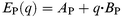
In order to extend this argument, orbital energies of the LUMO in a PTCDA molecule and the HOAO in a potassium atom, i.e.EP( q) and EK( q), respectively, were calculated as functions of nominal charge qe by the DV-Xα method, 32 where q is a real number not restricted to the integer and e is the elementary charge. Prior to these calculations the molecular geometry of PTCDA was optimized by the PM3 method. From the results of such density functional calculations it is clear that both EP( q) and EK( q) are expressed by linear functions of q in eqn. (3) and (4):
 | (3) |
 | (4) |
 | (5) |
Fig. 5 shows the comparison between one result thus obtained and the experimental one, which corresponds to the inverse of the result shown in Fig. 4, for δvs.n. These results are in good agreement with each other, while error bars for the observed points may be fairly long. Thus, this conformity leads us to conclude that the number of electrons transferred from potassium atoms to a PTCDA molecule in the thin film is predominantly regulated by the electronic reciprocation between the LUMO of the molecule and the HOAO of a potassium atom, with electron correlations involving Coulombic screening and repulsion in those atoms and molecules, even in the first approximation, neglecting probable interactions among the related electronic states of PTCDA molecules and potassium atoms.
 | ||
| Fig. 5 The number of electrons injected from potassium atoms to a PTCDA molecule as a function of potassium concentration. Comparison between the result observed from IPES (indicated by filled squares) and that calculated by eqn. (5) (shown by a solid curve). | ||
Thanks are due to Mr Masao Yoshikawa for providing pre-purified samples of PTCDA and DM-PBDCI and to Dr Hirohide Nakamatsu for his help in DV-Xα calculations. This work was supported in part by a Grant-in-Aid for Scientific Research No. 11304049 from the Ministry of Education, Science, Sports and Culture of Japan.
References
- P. D. Johnson and J. W. Davenport, Phys. Rev. B, 1985, 31, 7521 CrossRef CAS.
- N. Sato, H. Yoshida and K. Tsutsumi, J. Electron. Spectrosc. Relat. Phenom., 1998, 88–91, 861 CrossRef CAS.
- K. Yokoyama, K. Nishihara, K. Mimura, Y. Hari, M. Taniguchi, Y. Ueda and M. Fujisawa, Rev. Sci. Instrum., 1993, 64, 87 CrossRef CAS.
- H. Namatame, M. Tamura, M. Nakatake, H. Sato, Y. Ueda, M. Taniguchi and M. Fujisawa, J. Electron Spectrosc. Relat. Phenom., 1996, 80, 393 CrossRef CAS.
- K. Tsutsumi, H. Yoshida and N. Sato unpublished work. .
- H. Yoshida, K. Tsutsumi and N. Sato unpublished work. .
- P. W. Erdman and E. C. Zipf, Rev. Sci. Instrum., 1982, 53, 225 CrossRef.
- D. Straub and F. J. Himpsel, Phys. Rev. Lett., 1984, 52, 1922 CrossRef CAS.
- J. H. Weaver, J. L. Martin, T. Komeda, Y. Chen, T. R. Ohno, G. H. Kroll, N. Troullier, R. E. Haufler and R. E. Smalley, Phys. Rev. Lett., 1991, 66, 1741 CrossRef CAS.
- R. W. Lof, M. A. van Veenendaal, B. Koopmans, H. T. Jonkman and G. A. Sawatzky, Phys. Rev. Lett., 1992, 68, 3924 CrossRef CAS.
- J. J. Pireaux, R. Caudano and J. Verbist, J. Electron Spectrosc. Relat. Phenom., 1974, 5, 267 CrossRef CAS.
- K. Seki, S. Hashimoto, N. Sato, Y. Harada, K. Ishii, H. Inokuchi and J. Kanbe, J. Chem. Phys., 1977, 66, 3644 CrossRef CAS.
- H. Fujimoto, T. Mori, H. Inokuchi, N. Ueno, K. Sugita and K. Seki, Chem. Phys. Lett., 1987, 141, 485 CrossRef CAS.
- K. Seki, N. Sato and H. Inokuchi, Chem. Phys., 1993, 178, 207 CrossRef CAS.
- R. Dudde and B. Reihl, Chem. Phys. Lett., 1992, 196, 91 CrossRef CAS.
- N. Ueno and K. Sugita, Phys. Rev. B, 1986, 34, 6386 CrossRef CAS.
- N. Ueno, T. Fukushima, K. Sugita, S. Kiyono, K. Seki and H. Inokuchi, J. Phys. Soc. Jpn., 1980, 48, 1254 Search PubMed.
- Y. Hirose, C. I. Wu, V. Aristov, P. Soukiassian and A. Kahn, Appl. Surf. Sci., 1997, 113/114, 291 CrossRef CAS.
- N. Karl and N. Sato, Mol. Cryst. Liq. Cryst., 1982, 218, 79 Search PubMed.
- J. Danziger, J.-P. Dodelet, P. Lee, K. W. Nebesny and N. R. Armstrong, Chem. Mater., 1991, 3, 821 CrossRef CAS.
- Y. Hirose, W. Chen, E. I. Haskal, S. R. Forrest and A. Kahn, Appl. Phys. Lett., 1994, 64, 3482 CrossRef CAS.
- N. Sato and M. Yoshikawa, J. Electron Spectrosc. Relat. Phenom., 1996, 78, 387 CrossRef CAS.
- A. J. Lovinger, S. R. Forrest, M. L. Kaplan, P. H. Schmidt and T. Venkatesan, J. Appl. Phys., 1984, 55, 476 CrossRef CAS.
- S. R. Forrest, M. L. Kaplan and P. H. Schmidt, J. Appl. Phys., 1984, 55, 1492 CrossRef CAS.
- S. R. Forrest, L. Y. Leu, F. F. So and W. Y. Yoon, J. Appl. Phys., 1989, 66, 5908 CrossRef CAS.
- P. E. Burrows and S. R. Forrest, Appl. Phys. Lett., 1994, 64, 2285 CrossRef CAS.
- N. Karl, A. Bauer, J. Holzäpfel, J. Marktanner, M. Möbus and F. Stölzle, Mol. Cryst. Liq. Cryst., 1994, 252, 243 Search PubMed.
- P. Panayotatos, D. Parikh, R. Sauers, G. Bird, A. Piechowski and S. Husain, Solar Cells, 1986, 18, 71 Search PubMed.
- M. Hiramoto, H. Fujiwara and M. Yokoyama, J. Appl. Phys., 1992, 72, 3781 CrossRef CAS.
- E. Hädicke and F. Graser, Acta Crystallogr., Sect. C, 1986, 42, 189 CrossRef.
- M. Hasegawa and N. Sato, Mol. Cryst. Liq. Cryst., 1997, 296, 409 Search PubMed.
- H. Adachi, M. Tsukada and C. Satoko, J. Phys. Soc. Jpn., 1978, 45, 875 Search PubMed.
Footnote |
| † Basis of a presentation given at Materials Chemistry Discussion No. 2, 13–15 September 1999, University of Nottingham, UK. |
| This journal is © The Royal Society of Chemistry 2000 |