Nanometric electrostatic interfacial phenomena in organic semiconducting thin films†
Mitsumasa Iwamoto
Department of Physical Electronics, Tokyo Institute of Technology, 2-12-1 O-okayama, Meguro-ku, Tokyo, 152-8552, Japan, iwamoto@pe.titech.ac.jp
First published on UnassignedUnassigned22nd December 1999
Abstract
Surface potentials of two kinds of phthalocyanine Langmuir–Blodgett (LB) films deposited on metal electrodes were examined as a function of the number of deposited layers. It was found that the potential built across the LB films was due to the displacement of excessive electronic charges (electrons and holes) from metals. The spatial charge distribution in these LB films was determined to be of the order of nanometres in film thickness, and the distribution of the electronic density of states was also determined assuming the presence of both electron donating and accepting states at the metal/film interface. The capacitance–voltage (C–V) and current–voltage (I–V) characteristics of phthalocyanine LB films sandwiched between metal electrodes were examined taking into account the interfacial electrostatic phenomena.
1. Introduction
In recent years, many investigations have been carried out to build up tunnel junctions and molecular rectifying junctions using organic materials with the hope of observing novel and useful electrical and optical properties.1–3 For this purpose, it is essential to construct well-defined structures by incorporating almost pinhole free ultra-thin organic films between two metal electrodes. Till now, many organic materials including electrical insulating materials,4 semi-conducting materials5 and electrically conducting materials6 have been developed, and the current–voltage (I–V) characteristics of the junctions using these materials have been examined. However these are not sufficient. It is essential to clarify the interfacial electronic phenomena occurring at the metal/film interface, because the I–V characteristic of the junctions using ultra-thin films will be ruled by the nanometric interfacial phenomena. In addition, electrostatic interfacial phenomena have been a subject of continuous study in the fields of electrostatics and electrical insulation engineering since the discovery of contact electrification.7,8 It is believed that understanding the nanometric dielectric phenomena is essential for further development of electrical insulation engineering.9 Similarly it is believed that this understanding is a key for further development of commercialized organic materials applications such as electroluminescent diodes,10 liquid crystal displays,11 photocopying,12etc., and for the development of new organic ultra-thin film devices.13–15For understanding the interfacial electrostatic phenomena, it is obviously important to use ultra-thin films whose thickness is less than the electrostatic double layer, and to gain information on the distribution of the electronic density of states and the spatial charge distribution in the films.16 Thus, Langmuir–Blodgett (LB) films are suitable,17 because they can be prepared onto solid substrates by layer-by-layer deposition in the order of monolayer thickness.18 For example, electrically insulating polyimide (PI) LB films, with a monolayer thickness of 0.4 nm,4 are suitable for the study of electrification. On the one hand, semi-conducting phthalocyanine films are interesting and suitable from the viewpoint of electronics applications.5,19,20 Further, many electrically conductive LB films are interesting from the viewpoint of future electronic device applications such as molecular wires.6
It is also important to establish a method to gain information on the nanometric interfacial electrostatic phenomena. In the field of electrical insulation engineering, several non-destructive techniques have been developed to determine the space charge distribution in insulating thick films, e.g., polyethylene.21,22 Unfortunately, these measurements cannot be applied to the determination of spatial charge distribution in organic ultra-thin films, because the resolution of these measurements is restricted by the acoustic wave propagation velocity in the films, and the spatial resolution is limited to the order of micrometres. On the one hand, the interfacial phenomena in semi-conducting films have been clarified by capacitance–voltage (C–V) measurement.23 This measurement has an advantage in the detection of net excess charge flow at the metal/film interface. However we cannot determine the spatial charge distribution in ultra-thin films in a static state. The measurement of the ultra-thin films in a static state is crucially important in order to clarify the nanometric electrostatic interfacial phenomena. Therefore, in the present study, we employ surface potential measurement based on the Kelvin-probe method.16 Using this surface potential method, the relationship between the surface potential and the number of deposited LB layers is obtained. In our previous study,16,24 we examined the surface potential of electrically insulating PI LB films. We then revealed the presence of excessive electronic charges transferred from metals to PI LB films at the metal/PI LB film interface, and the formation of electronic space charge layers of the order of several nanometres at the interface. It was concluded that a very high density of electronic states of the order of 1025–1026 m−3 and very high electric field of the order of 108–109 V m−1 exist at the interface, due to the displacement of excess electrons from metals into the interfacial electronic states. Taking into account this nanometric interfacial electrostatic phenomenon, we analyzed the capacitance–voltage (C–V) and current–voltage (I–V) characteristic of ultra-thin PI LB films sandwiched between metal electrodes,25 and concluded that this interfacial phenomena give a direct effect on the electrical transport properties of PI LB films.
In this study, we pay attention to organic semiconductor films. We measure the surface potential of Cu-tetra(tert-butyl)phthalocyanine (CuttbPc) and octahexyloxyphthalocyanine-copper (C6PcCu) LB films which are deposited on various kinds of metal electrodes (Au, Cr, Al) as a function of the number of deposited layers. Subsequently we determine the spatial charge distribution formed at the metal/film interface, and then discuss the distribution of the electronic density of states. Finally, based on the information obtained here, we examine the electrical properties of metal–ultrathin film–metal elements using the C–V characteristics, and discuss the role of the nanometric interface in the electronic devices.
2. Experimental
2.1 Sample preparation and deposition for surface potential measurement
Cu-tetra(tert-butyl)phthalocyanine (CuttbPc) and octahexyloxyphthalocyanine-copper (C6PcCu) molecules, whose chemical structures are shown in Fig. 1, were used in this study. CuttbPc molecules were purchased from Wako Pure Chemical Industries Ltd., and then used as received without further purification. C6PcCu molecules were kindly supplied by Professor K. Ichimura of the Tokyo Institute of Technology. Both CuttbPc and C6PcCu molecules have one copper atom at the center of phthalocyanine rings. Firstly, we spread monolayers of C6PcCu (CuttbPc) on a pure water surface from a 0.29 mmol l−1 chloroform solution (1 mmol l−1 xylene solution) at a temperature of 20![[thin space (1/6-em)]](https://www.rsc.org/images/entities/char_2009.gif) °C. We then transferred the monolayers onto glass substrates covered with Au, Cr, or Al evaporated electrodes by the vertical dipping LB technique at a surface pressure of 27 mN m−1 and a molecular area of 90 Å2 at a temperature of 10°C. Similarly, monolayers of CuttbPc on a water surface were transferred onto glass substrates covered with Au, Cr, or Al evaporated electrodes by the horizontal lifting method at a surface pressure of 20 mN m−1 and a molecular area of 50 Å2 at 20 °C, except for the first layer which was deposited by the vertical dipping LB technique. The monolayer thickness of C6PcCu (and CuttbPc) LB films was determined to be 2.2 nm (and 1.7 nm) from the X-ray diffraction pattern of these LB films. In Fig. 1, the electrode configuration used for the surface potential measurement of CuttbPc and C6PcCu LB films is illustrated.
°C. We then transferred the monolayers onto glass substrates covered with Au, Cr, or Al evaporated electrodes by the vertical dipping LB technique at a surface pressure of 27 mN m−1 and a molecular area of 90 Å2 at a temperature of 10°C. Similarly, monolayers of CuttbPc on a water surface were transferred onto glass substrates covered with Au, Cr, or Al evaporated electrodes by the horizontal lifting method at a surface pressure of 20 mN m−1 and a molecular area of 50 Å2 at 20 °C, except for the first layer which was deposited by the vertical dipping LB technique. The monolayer thickness of C6PcCu (and CuttbPc) LB films was determined to be 2.2 nm (and 1.7 nm) from the X-ray diffraction pattern of these LB films. In Fig. 1, the electrode configuration used for the surface potential measurement of CuttbPc and C6PcCu LB films is illustrated. | ||
| Fig. 1 CuttbPc and C6PcCu molecules, and the electrode configuration of the samples used for the surface potential measurement. | ||
Before the surface potential measurement, all samples were heat-treated for more than one hour at a temperature of 70°C for C6PcCu LB films and at 150°C for CuttbPc LB films in a vacuum of the order of 10−6 Torr (1.33 × 10⁻⁴ Pa) for the purpose of removing water molecules adsorbed on the surface of samples and excess charges generated inside the samples. The surface potential measurement was carried out under vacuum (10−6 Torr). The surface potential of the LB films (at LB1, LB2 and LB3 in Fig. 1) was measured with reference to the potential of metal electrodes (at P in Fig. 1) by means of the conventional Kelvin method (Trek, Model 320B) using a probe electrode (5 mm2 electrode area) which is vertically vibrated with an amplitude of 0.2 mm at a frequency of 120 Hz. Firstly we placed this probe electrode above metal electrodes at a distance of 1 mm and measured the potential V0 of the metal electrode (at P in Fig. 1). Secondly, we moved the electrode to the position LB1, and then measured the potential V1 at this position in the same manner. Finally, we calculated the potential difference V1
−
V0 and defined it as the surface potential of the position LB1. In the experiment, the potential difference V1
−
V0 was directly measured and determined by adding the compensation voltage to the probe electrode. Temperature dependence of the surface potential was measured at various temperatures in the range −100 to 150°C on keeping the temperature for more than 1 hour before measurements.
2.2 Samples for I–V and C–V measurements
The Au/CuttbPc LB film/Al elements were prepared as follows. After the deposition of CuttbPc LB films as described in section 2.1, we carefully evaporated Al top electrodes at a vacuum of 10−6 Torr using a mechanical shutter. The electrode area S of the element was about 0.25 mm2 (0.5 mm × 0.5 mm). About 30–50% of the elements we made were not electrically shorted. It was found from optical microscope observation that the samples electrically shorted were shorted at the edge of the top Al electrodes with the bottom Au electrode, and the films themselves were not catastrophically damaged. Further, the reciprocal capacitance of Al/CuttbPc LB film/Al samples shows a linear relationship with the number of deposited layers (<20 layers) at a frequency of 1 kHz (not shown here). Thus we may argue that the deposited CuttbPc LB films are not catastrophically damaged by the evaporation of the top Al electrode. All of the successfully prepared Au/CuttbPc LB film/Al samples were annealed at a temperature of 100°C in a vacuum (10−6 Torr) before the electrical measurement. Current–voltage (I–V) characteristics of the samples were measured in a vacuum (10−6 Torr) at a temperature of 20°C by applying a triangular voltage with an amplitude V0 of 1.0 V and a frequency f0 of 2 mHz on to a Au bottom electrode with reference to the Al top electrode. The capacitance of the elements at a biasing voltage Vex was determined using the eqn. (1).26 | (1) |
Here, I+ and I− were the currents flowing through the circuit while a triangular applied voltage Vex increases and decreases, respectively.
3. Results and discussion
3.1 Spatial charge distribution and electron density of states
a. CuttbPc LB films. Fig. 2(a) shows the relationship between the surface potential of CuttbPc LB films on Au electrode and the number of deposited layers (n) at various temperatures. The surface potentials gradually increase as the number of deposited layers increases for n < 3. In contrast, the potentials gradually decrease as the number of deposited layers increases for n > 3, and the potentials reach saturated values in the range n = 10–20, indicating that the excess charges are displaced in the range within about 17–34 nm from the film/electrode interface. The saturated surface potential gradually decreases as the temperature decreases, and it changes the polarity at a temperature below 20
°C. Fig. 2(b) shows the surface potential of CuttbPc LB films on a Cr electrode. The surface potentials gradually decrease as the number of deposited layers increase, and they finally reach saturated potentials at n = 5. The surface potential gradually decreases as the temperature decreases in a manner similar to the surface potential change of CuttbPc on Au electrodes (see Fig. 2(a)). Fig. 2(c) shows the surface potential of CuttbPc LB films on Al electrodes. The surface potential gradually decreases as the number of deposited layers increases, and it reaches a saturated potential at around n = 8. Of interest is that the surface potential on Al electrodes becomes increasingly negative between 20 and 100°C. This is a major characteristic seen for CuttbPc LB films on Al electrodes, and this characteristic was not seen for CuttbPc LB films on Cr nor Au electrodes (see Figs. 2(a) and 2(b)). | ||
| Fig. 2 Relationship between the surface potential of the CuttbPc LB film and the number of deposited layers at various temperatures (a) on Au electrodes, (b) on Cr electrodes, (c) on Al electrodes. | ||
As mentioned, the surface potential across CuttbPc LB films depends on the metal of the base electrodes as well as the number of deposited layers. Similar results were obtained for PI LB films deposited on metal electrodes in our previous study,16,24 in which the surface potential built across PI LB films was due to the displacement of electrons from the metal electrodes, because the potential does not show a remarkable dependence of the base metal electrodes when the main contribution comes from the alignment of the constituent permanent dipoles in LB films. Further it is instructive here to note that the surface potential of LB films deposited on epitaxially grown Au electrodes shows a similar dependence with that of LB films deposited on Au evaporated electrodes.27 Thus the effect of the diffusion of Au atoms of the base electrode is negligible within the limit of our experiment. In the following, thus we argue that electronic charge exchange phenomena occur at the metal/CuttbPc film interface. Fig. 3 shows the relationship between work function of the metals and the saturated surface potential of CuttbPc LB films at 100, 20 and −100°C. Here, the work function of the Au electrode was determined as 4.75 eV from the ultraviolet photo-emission spectroscopy, and the work functions of Cr and Al were determined as 4.35 and 3.75 eV at 20°C by means of the contact potential method with reference to the potential of bare Au-evaporated electrode. The work functions of Cr and Al obtained by this contact method showed temperature dependence, and they were determined as 4.35 and 3.70 eV at 100°C, and 4.40 and 3.75 eV at −100°C, respectively. Linear relationships were observed between the work function of the metals and the saturated surface potentials. These linear relationships again suggest that electronic charge exchange occurs at the metal/film interface [see Fig. 5(a)].16 The surface potential of LB films should be zero when the surface Fermi-level of the films and the Fermi-level of the metals coincide. Therefore, judging from the value of the work function at the surface potential of V = 0.0 V in Fig. 3(a), we estimate that the surface Fermi level of CuttbPc LB films is located at electronic energy levels of 4.68, 4.75 and 4.94 eV below the vacuum level at temperatures of 100, 20 and −100°C, respectively. The surface Fermi-level of CuttbPc LB films shifts to a higher energy level as the temperature increases, indicating a characteristic behavior of so-called p-type semiconductors.23
 | ||
| Fig. 3 Relationship between the saturated surface potential across CuttbPc LB films and the work function of electrode materials at various temperatures. | ||
b. C6PcCu LB films. Fig. 4(a) shows the surface potential of C6PcCu LB films on Au, Cr and Al electrodes at 20
°C. The surface potentials depend on the metal electrodes and the number of deposited layers, indicating that excess charges are displaced from the metals into the LB films, in a manner similar to that of CuttbPc LB films. A surface potential with a positive polarity indicates the displacement of electrons from the LB films to the metals. In contrast, a potential with a negative polarity indicates transfer of electrons in the opposite direction. As shown in Fig. 4, the surface potential saturates when the number of deposited layers is about 10, indicating that the excess charges are displaced in the region within about 22 nm from the film/electrode interface. The saturated potential of C6PcCu is higher than that of CuttbPc at a temperature of 20°C [see Fig. 2(b)]. For example, the saturated surface potential of C6PcCu on an Au electrode is about 500 mV, whereas the potential of CuttbPc on an Au electrode is nearly zero. This result indicates that the CuttbPc LB film has a stronger tendency to accept electrons than does the C6PcCu LB film. It is interesting here to note that a small hump in the surface potential is seen for the CuttbPc LB films on Au electrodes, whereas it is not seen for the C6PcCu LB films. This difference is due to the difference of the distribution of the density of surface states as will be discussed in section 3.1.2. | ||
| Fig. 4 (a) Relationship between the surface potential of C6PcCu LB film and the number of deposited layers at 20°C. (b) Relationship between the saturated surface potential across C6PcCu LB films and the work function of electrode materials. | ||
Fig. 4(b) shows the relationship between the saturated surface potential and the work function of metal electrodes. A linear relationship with a slope of nearly unity is obtained, in particular at a temperature of 20°C for CuttbPc LB films as shown in Fig. 3, and also plotted in Fig. 4(b). For C6PcCu LB films, a similar linear relationship is obtained, where the slope is 0.6, not unity. These results indicate that electronic charges are exchanged at the metal/CuttbPc LB film interface until the surface Fermi level of the CuttbPc LB films and the Fermi level of the metals coincide. On the other hand, the electronic charge exchange occurs at the metal/C6PcCu LB film interface but the surface Fermi level of the C6PcCu LB film and the Fermi level of the metals do not coincide at the interface. One main reason is that the C6PcCu molecules have long-alkyl chains with an electric permanent dipole moment. Using the Maxwell displacement current measuring technique,28,29 the vertical component of the dipole moment of the C6PcCu monolayer on the water surface was determined as 4.0 D.27 Thus, there is a possibility that the electric dipoles of C6PcCu make a significant contribution to the build-up of the surface potential of C6PcCu LB films. In other words, the charge exchange is suppressed owing to the presence of dipole layers at the interface. Although the detail is not clear, we may expect from the results shown in Figs. 4(a) and (b) that the main contribution to the establishment of the surface potential of C6PcCu LB films is electronic charges (electrons and holes) which are displaced from metals. In the following, we determine the spatial charge distribution in CuttbPc and C6PcCu LB films.
 | (2) |
where D is the distance from the metal/film interface, and it is given by d−ΔD/2, where d is the film-thickness. In the LB technique, d is given by d = jΔD (j = 1, 2, 3, ..., n), where n is the number of deposited layers, εr is the relative permittivity of LB films, and ε0 is the permittivity of a vacuum. For CuttbPc LB films and C6PcCu LB films, εr was determined as 2.7 and 4.8 from the relationship between the reciprocal capacitance of these films and the number of deposited layers.
 | ||
| Fig. 5 (a) Schematic diagram of the displacement of electronic charges at the film/metal interface, and (b) schematic illustration of the electronic density of states at the interface. | ||
Fig. 6(a) shows the spatial charge distribution of CuttbPc LB films on Au, Cr and Al electrode at 20°C. Here the results were obtained from Fig. 2 by using eqn. (2). The spatial charge density ρ(x) steeply decreases as the number of layers n increases in the range n < 4. This result indicates that most of the excess charges displaced from metal electrodes exist within the first 3–4 deposited layers. The density of CuttbPc molecules is about 1.2 × 1027 m−3. Thus about 0.8% of CuttbPc molecules are expected to contribute to the charge exchange at the metal/film interface. It is instructive here to note that the polarity of the spatial charge density ρ(x) depends on the metal electrodes and the number of deposited layers. For example, in the range n = 1–3, the polarity of the charge density ρ(x) is positive for the Au electrode, whereas it is negative for the Al electrode. In other words, CuttbPc LB films have both electron donating and accepting states at the metal/film interface, and they accept electrons from Al electrodes and donate electrons to Au electrodes.
 | ||
| Fig. 6 Spatial charge distribution in LB films at a temperature of 20°C: (a) CuttbPc LB film, and (b) C6PcCu LB film. | ||
Fig. 6(b) shows the spatial charge distribution in C6PcCu LB films. Similarly, space charges with very high density are accumulated in the first and second LB layers, and the spatial charge density steeply decreases as n increases. These results suggest that many electron donating or accepting states exist in LB films at the metal/film interface. It is estimated that about 3% of the C6PcCu molecules in the first layer accept one electron from the Au electrodes, assuming that the density of C6PcCu molecules in the LB film is 5.1 × 1026 m−3.
 | (3) |
Here f(E) is the Fermi–Dirac distribution function, and e is charge on an electron. E represents the depth of the electron energy state with respect to the vacuum level (V.L.). nA and nD are the density of electron accepting and donating states (D.O.S.), which work to accept electrons and to donate electrons, respectively. Wm represents the work function of the metal electrode and Vs is the electrostatic potential at position x in LB film.
As shown in Fig. 6(a), CuttbPc LB films on Au are positively charged at a temperature of 20°C, whereas the films on Al and Cr electrodes are negatively charged. This result suggests that electron donating states of CuttbPc LB films extend into the energy level which is higher than the Fermi level of an Au electrode, whereas electron accepting states extend into the energy level which is lower than the Fermi level of Al electrodes (see Fig. 5(b)). Thus, we conclude that electron donating states mainly make a contribution to the build up of surface potential Vs for CuttbPc LB films on Au electrodes, whereas electron accepting states mainly contribute to CuttbPc LB films on Cr and Al electrodes. In other words, eqn. (3) is approximately rewritten as eqn. (4.a)
 | (4a) |
for positively charged CuttbPc LB films on an Au electrode, assuming that the Fermi–Dirac distribution function f(E) is approximately given by a step function varying around the Fermi level of metals. Similarly, eqn. (3) is approximately rewritten as eqn. (4.b)
 | (4b) |
for negatively charged LB films on Al and Cr electrodes. In eqns. (4.a) and (4.b), E0 represents the Fermi level of the metal with reference to the vacuum level, and it is given by E0 = − Wm + eVs (see Fig. 5(a)). In other words, the position E0 shifts due to the electrostatic potential Vs in films. Similar arguments hold for the result of surface potential of CuttbPc LB films at various temperatures (not shown), except that the electron accepting states become dominant as the temperature decreases (see Fig. 2). The G(E0,x,T) of CuttbPc and C6PcCu LB films was calculated in a manner similar to that described in our previous paper.24
Figs. 7(a) and (b) show the G(E0,x,T) of CuttbcPc and C6PcCu LB films, respectively. Curves 1L, 2L, 3L, and 4L represent the G(E0,x,T) at positions of x = 0.5ΔD, 1.5ΔD, 2.5ΔD and 3.5ΔD, respectively. Solid lines with open circles represent the G(E0,x,T) for electron accepting states, and broken lines with closed circles for electron donating states. The marks (Al), (Cr) and (Au) indicated in Fig. 7(a) represent the G(E0,x,T) which are estimated from the data of the CuttbLB films on Al, Cr and Au shown in Fig. 6(a), respectively. Similarly, the G(E0,x,T) was estimated for C6PcCu LB films in Fig. 7(b). It is found that very high-density electron accepting and donating states exist at the first monolayer of CuttbPc and C6PcCu LB films. Further, G(E0,x,T) decreases steeply as the number of deposited layers increases. From this figure, it is expected that the Fermi level of C6PcCu is located at an energy of 4.0 eV and that of CuttbPc at 4.7 eV from the vacuum level at the interface (see curve 4L). Thus we may argue that CuttbPc LB films have a stronger tendency to accept electrons from metal electrodes than do the C6PcCu LB films. Further, we could conclude that a small hump in the surface potential seen for the CuttbPc LB films on Au electrodes is due to the difference of the distribution of density of surface states which extend around the Fermi level of these films. As mentioned above, we explained our experimental results assuming the presence of both electron-accepting and donating states at the interface.
 | ||
| Fig. 7 Relationship between G(E0,x,T) and the energy E0 at a temperature of 20°C: (a) CuttbPc LB film, and (b) C6PcCu LB film. | ||
3.2 C–V and I–V characteristics of Au/CuttbPc/Al elements
Discussions for CuttbPc LB films will run in a manner similar to those for C6PcCu LB films. Thus, in the following, we confine our discussion to Au/CuttbPc LB films/Al elements. As mentioned in section 3.1, CuttbPc LB films are charged due to the excess charges displaced from the metal electrodes. Thus the electric flux diverging from the excess charges falls on the metal electrodes, and the electrostatic potential Vs′ is built across the films. Vs′ is given by eqn. (5).16 | (5) |
Here Ds is the thickness of space charge layer in the metal/CuttbPc LB film interface. Thus we expect the Au/CuttbPc/Al elements are charged in a manner as shown in Fig. 8(a), when Au and Al electrodes are electrically shorted, because a negatively charged layer is formed at the Al/CuttbPc LB film interface and a positively charged layer is formed at the Au/CuttbPc LB film interface. The thickness of the negatively charged layer and of the positively charged layer are estimated to about 10 nm and 3 nm from Fig. 6(a). The spatial charge density ρ(x) at the position x from the Al electrode is expressed by eqn. (3). On the one hand, when an external voltage Vex is applied to the top Au electrode with reference to the upper Al electrode, the thickness of space charge layer will be changed as shown in Figs. 8(b) and (c), because the application of Vex will produce the additional spatial charge density Δρ(Ds) at the metal/CuttbPc LB film interface. The relationship between the applied voltage and the spatial charge density ρ(x) at the Al/CuttbPc LB film interface is given by eqn. (6) under the following assumptions: (i) redistribution of charges in films in the region of 0 < x < Ds is negligibly small, and (ii) the applied voltage Vex is added to the space charge layer at the Al/CuttbPc LB film interface.
 | ||
| Fig. 8 Energy diagram Au/CuttbPc LB film/Al element (a) in a short circuit condition (Vex = 0), (b) Vex > 0, and (c) Vex < 0. | ||
 | (6) |
Here, ρ(x) is the spatial charge density at the position x from the Al upper electrode. Vs is the electrostatic potential built across the Al/CuttbPc LB film interface when Vex = 0. The thickness of the space charge layer increases for Vex < 0, whereas it decreases for Vex > 0. Differentiating eqn. (6) with respect to Ds, we obtain the relationship between the spatial charge density ρ(Ds) and the capacitance C, which is given by eqn. (7)23
 | (7) |
assuming that the negatively charged Al/CuttbPc LB film layer functions as an insulating layer, and the capacitance per unit area of Au/CuttbPc LB film/Al element is expressed by C = ε0εr/Ds.
Fig. 9 shows the I–V, C–V and 1/C2–V characteristics of the Au/CuttbPc LB film/Al element at a frequency of 2 mHz. The I–V characteristic shows a rectifying behavior similar to a Schottky-type diode,23 and the current I increases steeply for Vex > 0. Further, the capacitance increases as the applied voltage Vex increases in the range −0.5 < Vex < 1.0 V. The I–V and C–V characteristics do not depend on the film thickness in the range −1.0 < Vex < +0.5 V. From the electrical measurement, we found that the Al/CuttbPc LB film interface has a very high electrical resistance of an order of 1014 Ω cm, whereas the bulk and/or Au/CuttbPc LB film interface have a relatively small resistance of an order of 108 Ω cm. Therefore it is expected that the applied field Vex is added to the Al/CuttbPc interfacial layer, and that the Al/CuttbPc LB film interfacial layer efficiently blocks current flowing across the film in the range −1.0 < Vex < +0.5 V. From eqn. (1) and Fig. 9(b), the thickness of the insulating layer is estimated to about 11 nm at zero bias, and this film thickness just corresponds to the thickness of the negatively charged layer at the Al/CuttbPc LB film interface. The thickness of the Al/CuttbPc insulating layer Ds decreases as Vex increases, where Ds is 15 nm in the maximum. The capacitance and current increase gently in the range Vex < −0.5 V. As mentioned in section 3.1, the Fermi level of CuttbPc LB films is located at an energy of 4.7 eV, whereas the highest occupied molecular orbital (HOMO) level of CuttbPc LB films is estimated to be located at an energy of 5.2 eV from the cyclic voltammetry measurement (not shown here). Thus for Vex < −0.5 V, the HOMO level becomes higher than the Fermi level of Al electrode, and a very high electric field with an order of 106 V cm−1 is applied to the Al/CuttbPc LB film interface. Therefore at the Al/CuttbPc LB film interface, the current is allowed to flow in the range Vex < −0.5 V, probably due to the electron tunneling or hole injection between the HOMO level of CuttbPc LB film and the Al electrode (see Fig. 8 (c)).
 | ||
| Fig. 9 The electrical characteristics of Au/CuttbPc LB film/Al elements: (a) I–V, (b) C–V, and (c) 1/C2–V (Voltage represents Vex). | ||
In Fig. 9(c), the 1/C2 increases gradually as Vex decreases in the range −0.2 < Vex < +0.4 V. A slope of the 1/C2–V characteristic gives the density of electron accepting states, and the density is calculated using eqn. (7) and Fig. 9(c). Fig. 10 shows the result obtained. We also plotted the distribution of spatial charge density obtained using the surface potential measurement by a solid line. It is interesting to note that the distribution of ρ(Ds) obtained by capacitance measurement agrees with that obtained by surface potential measurement for 3 < Ds < 10 nm, suggesting that most of the excessive electronic charges in this region can move by application of the external voltage with a frequency of the order of mHz. On the contrary, the values of ρ(Ds) are scattered in the range Ds ∼ 3 nm and the distribution of ρ(Ds) can not be estimated, possibly due to the increase of the leakage current in our experiment. It is interesting here to note that the thickness of Ds ∼ 3 nm corresponds to the thickness of the first two-molecular layer. Thus, from the viewpoint of the determination of the spatial distribution, it is concluded that the surface potential method is more helpful to determine the distribution in the range within several nanometres from the interface. However, from the viewpoint of device operation, information on the charge exchange at the interface is required and the C–V measurement is helpful. Therefore, the combination of the surface potential method and C–V measurement will be important for further development of organic molecular devices.
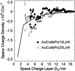 | ||
| Fig. 10 The spatial charge distribution of the Al/CuttbPc LB film interface determined from the C–V measurement and the surface potential measurement (solid line). | ||
4. Conclusion
We examined the surface potential Vs of CuttbPc and C6PcCu LB films deposited on Al, Cr and Au electrodes, and then concluded that the displacement of electronic charges between metal electrodes and film is responsible for the establishment of Vs. The spatial charge distribution in these LB films was determined to be on the nanometre scale, and the distribution of the electronic density of states was also determined. We finally concluded the interfacial phenomena and the electrical properties of ultra-thin films sandwiched between electrodes can be explained by assuming the presence of both electron donating and accepting states in CuttbPc LB films.References
- F. L. Carter, Molecular Electronic Devices II, Marcel Dekker, Inc., New York, 1987. Search PubMed.
- Special Issue, “Nano-Molecular Electronics", Jpn. J. Appl. Phys., 1995, 34..
- Proceedings of the ‘Nano-molecular Electronics International Workshop '97', Kobe, Japan, 10–11 December 1997, ed. M. Iwamoto and S. Mashiko, Thin Solid Films, 1998, 331. Search PubMed.
- M. IwamotoM. Kakimoto, “Polyimides as Langmuir-Blodgett films", in Polyimides, Fundamentals and Applications, ed. Malay K. Ghosh and K. L. Mittal, Marcel Dekker, Inc., New York, 1996, ch. 25. Search PubMed.
- G. Roberts “Potential Applications of Langmuir–Blodgett Films", in Langmuir–Blodgett Films, ed. G. Roberts, Plenum Press, New York, 1990, ch. 7. Search PubMed.
- T. Nakamura, in Handbook of Organic conductive molecules and polymers. Vol. 1 Charge transfer salts, Fullerenes and photoconductors, ed. H. S. Nalwa, John Wiley & Sons Ltd., New York, 1997, ch.14, p. 727. Search PubMed.
- J. LowellA. C. Rose-Innes, Adv. Phys., 1980, 29, 947, and references cited therein. Search PubMed.
- L. H. Lee, J. Electrostat., 1994, 32, 1, and references cited therein. Search PubMed.
- T. J. Lewis, IEEE Trans. Dielectr. Electr. Insul., 1994, 1, 812 CrossRef CAS.
- L. S. Hung, C. W. Tang and M. G. Mason, Appl. Phys. Lett., 1997, 70, 152 CrossRef CAS.
- A. A. Sonin, The surface physics of liquid crystals, Gordon and Breach Publishers, Amsterdam, 1995. Search PubMed.
- P. K.Watson, IEEE Trans. Dielectr. Electr. Insul., 1995, 2, 915, and references cited therein. Search PubMed.
- K. KanetoK. KudoY. OhmoriM. OnodaM. Iwamoto, IEICE Trans. Electron., 1998, E81-C, 1009. Search PubMed.
- E. G. Wilson, Jpn. J. Appl. Phys., 1995, 34, 3775 CrossRef CAS.
- K. Takimoto, R. Kuroda, S. Shido, S. Yasuda, H. Matsuda, K. Eguchi and T. Nakagiri, J. Vac. Sci. Technol. B, 1997, 15, 1429 CrossRef CAS.
- M. Iwamoto, A. Fukuda and E. Itoh, J. Appl. Phys., 1994, 75, 1607 CrossRef CAS.
- G. L. Gaines, Insoluble Monolayers at Liquid-Gas Interfaces, Interscience, New York, 1965. Search PubMed.
- M. C. Petty, Langmuir–Blodgett Films: an introduction, Cambridge University Press, Cambridge, 1996. Search PubMed.
- C. C. LeznoffA. B. P. Lever, Phthalocyanines–Properties and Applications, VCH Publishers, Weinheim, 1989. Search PubMed.
- (a) C. M. Fischer, M. Burghard, S. Roth and K. v. Klitzing, Europhys. Lett., 1994, 28, 129 Search PubMed; (b) Appl. Phys. Lett. 1995663331 Search PubMed.
- G. M. Sessler, IEEE Trans. Dielectr. Electr. Insul., 1998, 4, 614 CrossRef.
- N. H. Ahmed and N. N. Srinivas, IEEE Trans. Dielectr. Electr. Insul., 1998, 4, 644 CrossRef.
- S. M. Sze, “Metal-Semicondoctor Contacts", in Physics of Semiconductor Devices, Wiley Press, New York, 1981, ch. 5. Search PubMed.
- (a) E. Itoh and M. Iwamoto, J. Appl. Phys., 1997, 81, 1790 CrossRef CAS; (b) Appl. Phys. Lett. 1996682714 Search PubMed.
- E. Itoh and M. Iwamoto, J. Appl. Phys., 1999, 85, 7239 CrossRef CAS.
- A. J. Twarowski and A. C. Albrecht, J. Chem. Phys., 1979, 70, 2255 CrossRef CAS.
- E. Itoh and M. Iwamoto, J. Electrostat., 1996, 36, 313 Search PubMed.
- (a) M. Iwamoto, Y. Majima, H. Naruse, T. Noguchi and H. Fuwa, Nature, 1991, 353, 645 CrossRef CAS; (b) J. Chem. Phys. 1991958561 Search PubMed.
- M. Iwamoto and Y. Majima, J. Chem. Phys., 1991, 94, 5135 CrossRef CAS.
- T. J. Fabish and C. B. Duke, J. Appl. Phys., 1994, 75, 1607 CrossRef CAS.
Footnote |
| † Basis of a presentation given at Materials Chemistry Discussion No. 2, 13–15 September 1999, University of Nottingham, UK. |
| This journal is © The Royal Society of Chemistry 2000 |