Organic electroluminescent devices: enhanced carrier injection using SAM derivatized ITO electrodes†
Susan F. J. Appleyard, Stephen R. Day*, Richard D. Pickford and Martin R. Willis
Molecular Electronics Lab., School of Chemistry, University of Nottingham, Nottingham, UK NG7 2RD
First published on UnassignedUnassigned22nd December 1999
Abstract
Taking as a device model ITO|TPD|Alq3|Al (where TPD is N,N′-bis(3-methylphenyl)-N,N′-diphenyl-1,1′-biphenyl-4,4′-diamine and Alq3 is tris(quinolin-8-olato)aluminium) it is shown that control and improvement of carrier injection may be achieved using self-assembled monolayers (SAMs) to manipulate the Schottky energy barrier at the ITO–TPD interface. By using polar adsorbate molecules with the dipole oriented outward from the surface an artificial dipolar layer is formed and the work function is increased, and viceversa. With this method the threshold voltage for light emission (turn-on) can be reduced by 4 V and the maximum luminance increased by a factor of 3.5, giving an overall performance superior to that using the more stable Ag/Mg counter electrode. The SAMs effect is confirmed using a Scanning Kelvin Probe (SKP) to profile the relative work function of half-coated ITO samples. Increases in work function in excess of 0.3 eV are observed, in line with predictions using the calculated molecular dipoles of the SAM molecules.
Organic electroluminescent devices (OEDs) based on either thin films of polymers or lower molecular weight materials show increasing promise as commercial devices for use in full colour, flat panel displays. However, some problems still remain, particularly the high operating voltage, low efficiency and short device lifetime.1
The performance of the OEDs is strongly influenced by the conditions at both electrodes, under which carrier injection takes place. The rate of injection into a bilayer device depends on the position of the work function of the electrode relative to the appropriate band of the adjacent organic layer, the field distribution within the device and the quality of the contact. The electron injecting electrode requires a low work function metal such as magnesium or calcium. However, these materials tend to be readily oxidised, a factor which limits device lifetime. Aluminium is more stable but has a higher work function. Conversely, for hole injection, a high work function is required. Since it is generally necessary for this electrode to be optically transparent, indium tin oxide (ITO) coated glass is almost universally used. Although its work function has been found to be as high as 5.15 eV it appears that there may still be a barrier to hole injection.
In response, much work has been published on methods to improve the injecting properties of the electrodes. In the case of aluminium, it has been reported that a thin (5–24 Å thick) insulating buffer layer, such as LiF2 or Al2O3,3 between the aluminium electrode and the emitter layer can dramatically enhance the electron injection and the efficiency of OEDs. The improvement has been attributed to the removal of trapping states at the interface and better alignment of the metallic Fermi level with the conduction band of the emitter. Multilayer Langmuir–Blodgett films have also been used with similar effect.4,5 Work with ITO has concentrated on the use of plasma6–8 and aqua regia8,9 treatments to improve carrier injection. Increased performance is believed to be due to the elimination of surface contaminants, improved contact with the hole transport layer because of changes in surface morphology, and a change in the work function.
It is known that the work function of a metal is influenced by the electrostatic conditions at its surface.10 Using this effect, Zehner11,12 and Campbell13,14 have recently shown that dipolar arenethiols form self-assembled monolayers on gold and can be exploited to control the work function. This suggests that SAM modified electrodes could greatly enhance the performance of OEDs. Taking as a model device ITO|TPD|Alq3|Al, SAMs can be incorporated at the ITO–TPD interface. It has been demonstrated that both carboxylic acid, and preferably phosphonic acid (PA) derivatives, form SAMs on ITO.15 Nüesch et al.16 observed improved performance in single layer polymer devices using a carboxylic acid functionalised oligomer monolayer grafted to the ITO electrode. They interpreted this effect as being due to reduced pinhole formation at the interface as well as an increase in the ITO work function.
Using a similar approach we demonstrated that pre-treatment of the ITO electrode with a dipolar phosphonic acid, (2-chloroethyl)phosphonic acid, greatly enhanced the performance of the device, most notably by reduction of the turn-on. Preliminary results were published in a conference report.17 This paper contains a more detailed study covering a wider range of compounds and includes measurement of the effect on the work function using a Scanning Kelvin Probe (SKP). Most significantly, (4-nitrophenyl)phosphonic acid increases the work function by more than 0.3 eV and reduces the turn-on voltage by 4 V giving a device performance superior to that with the Mg/Ag counter electrode.
Experimental
Substrate preparation
The substrate (precoated ITO glass) was purchased from Balzers (Baltracom 247 ITO, 1.1 mm thick) with a sheet resistance and transmittance of 20 Ω sq−1 and 90% respectively. This was cut into 20 × 25 mm sample slides. | ||
| Fig. 1 Basic three-cell, bilayer device structure used in the study. | ||
 | ||
| Fig. 2 Molecular structures of the four SAM adsorbates used in the study. 1. (trichloromethyl)phosphonic acid (TCPA), 2. (4-nitrophenyl)phosphonic acid (4-NPPA), 3. (aminomethyl)phosphonic acid (AMPA), and 4. (2-chloroethyl)phosphonic acid (2-CEPA). | ||
Solutions of each PA (1 × 10⁻⁴ M) were prepared in 30% methanol in chloroform (30MCF), with the exception of AMPA for which an aqueous solution was used. For device fabrication, the slides were derivatized with a SAM by immersion in a solution of the appropriate PA, typically for a period of 16 hours. For the SKP measurements only half of the slide was treated. After derivatization, the slides were removed from solution and rinsed thoroughly with fresh 30MCF. The presence of each PA on the ITO surface was confirmed by measuring the advancing contact angle relative to bare ITO of triply distilled water on the surface (Table 1). Our previous work has verified the adsorption of similar PAs on ITO using Secondary Ion Mass Spectroscopy (SIMS)18 and Electron Paramagnetic Resonance (EPR).19
| Substrate | Contact angle/° using triply distilled water |
|---|---|
| ITO (as received) | 73 ± 2 |
| ITO|(2-chloroethyl)phosphonic acid | 49 ± 2 |
| ITO|(aminomethyl)phosphonic acid | 55 ± 2 |
| ITO|(trichloromethyl)phosphonic acid | 64 ± 2 |
| ITO|(4-nitrophenyl)phosphonic acid | 67 ± 3 |
Devices
 | ||
| Fig. 3 N,N′-Bis(3-methylphenyl)-N,N′-diphenyl-1,1′-biphenyl-4,4′-diamine (TPD). | ||
 | ||
| Fig. 4 Tris(quinolin-8-olato)aluminium (Alq3). | ||
Following fabrication the devices were transferred immediately from the vacuum chamber for characterisation. The current–voltage (I–V) and luminance–voltage (L–V) characteristics were recorded under forward bias using a Keithley 195 electrometer, a Thurlby PL320 power source and a Macam Q102 radiometer interfaced to a personal computer. The characteristics of the three cells were then averaged.
Work function measurements
The sample was mounted on a micromanipulator arm within a vacuum system such that the surface could be scanned across the face of the reference electrode using a stepper motor controlled by a personal computer. The entire SKP assembly, controller software and electronics were designed and built in the School of Chemistry at the University of Nottingham. Typical performance of the SKP showed noise levels of <1 mV (∼ 0.3% of the values measured) and a drift of < 5 mV h−1 at a resonant frequency of 237 Hz using a vibration amplitude of ∼1.0 mm when operating under medium vacuum (2 × 10⁻⁶ mbar) conditions. The scan sequence consisted of five averaged probe readings taken at 100 points along the 25 mm length of the slide. The scans were repeated three times and averaged to produce a final differential work function profile for the slide. By scanning a slide partially treated with a SAM, the difference in work function between treated and untreated ITO is determined directly, obviating the need for a separate reference surface of known work function.
Results and discussion
Scanning Kelvin Probe studies
Fig. 5 shows the SKP profiles for both the bare and partially treated substrates. The effect of the monolayers is seen as a shift in the relative contact potential approximately midway across the substrate. In an idealised situation we would expect to see a sharp step function at the transition between the treated and untreated regions of the substrate. However, the limited linear resolution of the probe together with surface concentration effects in the derivatisation solution mean that this step is significantly broadened. | ||
| Fig. 5 Relative work function profiles for each partially treated substrate: (a) no SAM, (b) 4-NPPA, (c) TCPA, (d) 2-CEPA and (e) AMPA. | ||
It was first necessary to determine the immersion time required for complete monolayer formation and hence to reproduce the maximum effect on the work function. A study of a series of slides treated over a 24-hour period is shown in Fig. 6 for the case of (2-chloroethyl)phosphonic acid. 16 hours was therefore adopted as the derivatisation time.
 | ||
| Fig. 6 Dependence of Δϕ on immersion time for 2-(chloroethyl)phosphonic acid. | ||
Following immersion it is desirable to wash the slide in excess pure solvent to prevent recrystallisation of the PA on the surface. This is a process that takes only a few seconds. Measurements after extended washing periods show that the PA molecules slowly desorb, confirming the necessity for rapid washing. This may be of importance in connection with electrode patterning. If a photoresist mask were to be used, for example, the solvent for its removal would need to be one in which the PA was insoluble.
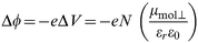
The work function shift Δϕ induced by a uniform dipolar surface layer is determined by the change in electrostatic potential (ΔV) created at the surface (Fig. 7) and can be derived from classical electrostatics as eqn. (1),
 | ||
| Fig. 7 Variation in electrostatic potential in a surface dipolar layer. Here the dipole is directed into the surface reducing the work function. ΔV can be calculated using eqn. (1). | ||
 | (1) |
where N is the surface number density (taken to be 1.7 × 10⁻¹⁴ cm−2 as determined by Wrighton15), εr is the dielectric constant of the SAM (taken to be 2.513,14,26), and μmol⊥ is the molecular dipole normal to the surface (defined as positive when pointing inwards). Table 2 shows the average empirical work function shift Δϕ and the calculated molecular dipoles with the corresponding predicted work function shift.
| SAM | Work function change, Δϕ /eV | Calculated dipole, μmol⊥ /D | Calculated work function change, Δϕ /eV |
|---|---|---|---|
| 4-NPPA | 0.303 | 5.73 | 0.720 |
| TCPA | 0.185 | 1.76 | 0.221 |
| 2-CEPA | 0.179 | 1.69 | 0.212 |
| AMPA | −0.140 | −1.43 | −0.179 |
Using this simple model, the changes in work function are in the same sequence and direction as those predicted by the calculations, despite the approximations involved. In particular, when the direction of the dipole is reversed so too is the direction of change of the work function, suggesting that the effect is, at least to a first approximation, as described by the model in eqn. (1). More accurate calculations require knowledge of the molecular conformation, coverage, the molecular order of the monolayer, and the nature of the bonding to the surface, as well as an accurate value of the dipole moment in the adsorbed state.
Device studies
The L–V and I–V plots are given in Fig. 8 and 9 respectively. The most significant characteristics are summarised in Table 3. | ||
| Fig. 8 Luminance–voltage characteristics for devices using: (a) 4-NPPA, (b) TCPA, (c) 2-CEPA, (d) no SAM, and (e) AMPA. | ||
 | ||
| Fig. 9 Current–voltage characteristics for devices using: (a) 4-NPPA, (b) TCPA, (c) no SAM, and (d) AMPA. | ||
| Device | Threshold voltage/V | Max. luminance/cd m−2 | Drive voltage @ 300 cd m−2/V | Q.E. @ 300 cd m−2 (%) | L.E. @ 300 cd m−2/lm W−1 |
|---|---|---|---|---|---|
| 4-NPPA | 2.0 | 13 120@14 V | 7.88 | 0.91 | 1.28 |
| TCPA | 2.0 | 9037@15.6 V | 8.82 | 0.69 | 0.81 |
| 2-CEPA | 4.0 | 7120@15.7 V | 9.51 | 0.63 | 0.92 |
| No SAM | 6.0 | 3640@20.5 V | 13.60 | 0.61 | 0.56 |
| AMPA | 9.5 | 3010@20 V | 15.50 | 0.46 | 0.30 |
The I–V plots show that the SAMs have a significant effect on the magnitude of the injected current. In the L–V plots for the 4-NPPA, TCPA and 2-CEPA SAMs there is a dramatic improvement in the luminance threshold voltage over the basic device, to the extent that the performance is superior to devices using Mg/Ag as the counter electrode.17 This suggests that there is a considerable effect on the Schottky barrier attributable to the dipole of the surface molecules. This is further confirmed by the adverse effect of the AMPA SAM. Since the turn-on voltage is governed by the onset of two-carrier injection, this also indicates that, in the aluminium device, injection of holes from the ITO anode occurs secondary to injection of electrons from the cathode. It is noted, however, that while the 4-NPPA device does exhibit improved luminance and efficiency, there is no significant decrease of the luminance threshold over the TCPA device despite significantly different dipole moments. This may imply that the conditions have been met whereby the work function of the ITO is greater than that of the TPD such that the contact becomes ohmic. As such, a further increase in work function would not necessarily result in a lower threshold. The work function of ITO has been reported to be 4.5–5.15 eV, however, accurate values of the TPD Fermi level are to the best of our knowledge not available. However the energy of the HOMO has been measured to be around 5.4 eV. This suggests a barrier height of approximately 0.25 eV when bare ITO is used. Alternatively, this may indicate that below some critical barrier height, the ITO becomes the primary injection electrode and the turn-on voltage is now determined by the Al electrode. Consequently there is no net reduction in threshold with further increase of the ITO work function. Nevertheless, assuming that electrons are the dominant carrier, there will still be an accompanying increase in hole injection leading to higher recombination efficiency and light output.
The introduction of a monolayer at the ITO interface will also have consequences for the internal field distribution, which may be beneficial for hole injection. Indeed, it becomes necessary to invoke an explanation that considers the field distribution within the device in order to explain the effect of SAMs on the Mg/Ag device. Our previous work17 has shown that SAMs on ITO produce only a minor reduction in threshold when Mg/Ag is the counter electrode. Our proposed explanation is based on a dynamic voltage dependent internal field distribution. If the device is viewed as a set of resistances in series representing the interfaces, at low voltages the potential difference is predominantly across the more resistive electrode. As the voltage is increased the more resistive electrode becomes injecting and the potential difference starts to increase across the other electrode until this becomes injecting. This is the threshold for two carrier injection and hence light emission. Thus, the threshold corresponds to the voltage for the onset of injection at the less resistive electrode. When Mg/Ag is used, the more resistive electrode at low voltages is assumed to be the ITO. The use of a SAM on the ITO improves its hole injection, and reduces its resistance, but not below that of the Mg/Ag. Consequently, the effect is small. The situation is very different when aluminium is the electron injecting electrode. The higher work function and the presence of an oxide layer make this the more resistive electrode at low voltages. The turn-on voltage is now determined by the ITO. Enhancement of its hole injecting properties by the use of a SAM therefore has a more dramatic effect.
Conclusion
Self-assembled monolayers of dipolar phosphonic acids adsorbed onto the surface of ITO glass provide a cheap and simple way of modifying the work function. Measurements using a Scanning Kelvin Probe show that the changes are of magnitude and direction broadly as predicted from theory. Electroluminescent devices using the modified electrodes show greatly enhanced performance particularly in threshold voltage.References
- J. R. Sheats, H. Antoniadis, M. Hueschen, W. Leonard, J. Millar, R. Moon, D. Roitman and A. Stocking, Science, 1996, 273, 884 CrossRef CAS.
- L. S. Hung, C. W. Tang and M. G. Mason, Appl. Phys. Lett., 1997, 70, 152 CrossRef CAS.
- F. Li, H. Tang, J. Anderegg and J. Shinar, Appl. Phys. Lett., 1997, 70, 1233 CrossRef CAS.
- M. Jin and G. Wang, Jpn. J. Appl. Phys., 1997, 36, L30 CrossRef CAS.
- Y.-E. Kim, H. Park and J.-J. Kim, Appl. Phys. Lett., 1996, 69, 599 CrossRef CAS.
- K. Furukawa, Y. Terasaka, H. Ueda and M. Matsumura, Synth. Met., 1997, 91, 99 CrossRef CAS.
- C. C. Wu, C. I. Wu, J. C. Sturm and A. Kahn, Appl. Phys. Lett., 1997, 70, 1348 CrossRef CAS.
- J. S. Kim, M. Granström, R. H. Friend, N. Johansson, W. R. Salaneck, R. Daik, W. J. Feast and F. Cacialli, J. Appl. Phys., 1998, 84, 6859 CrossRef CAS.
- F. Li, H. Tang, J. Shinar, O. Resto and S. Z. Weisz, Appl. Phys. Lett., 1997, 70, 2741 CrossRef CAS.
- P. A. Cox, The Electronic Structure & Chemistry of Solids, Oxford University Press, 1987, p. 231. Search PubMed.
- R. W. Zehner, B. F. Parsons, R. P. Hsung and L. R. Sita, Langmuir, 1999, 15, 1121 CrossRef CAS.
- A.-A. Dhirani, R. W. Zehner, R. P. Hsung, P. Guyot-Sionest and L. R. Sita, J. Am. Chem. Soc., 1996, 118, 3319 CrossRef CAS.
- I. H. Campbell, S. Rubin, T. A. Zawodzinski, J. D. Kress, R. L. Martin, D. L. Smith, N. N. Barashkov and J. P. Ferraris, Phys. Rev. B, 1996, 54, 14321 CrossRef CAS.
- I. H. Campbell, J. D. Kress, R. L. Martin, D. L. Smith, N. N. Barashkov and J. P. Ferraris, Appl. Phys. Lett., 1997, 71, 3528 CrossRef CAS.
- T. J. Gardner, C. D. Frisbie and M. S. Wrighton, J. Am. Chem. Soc., 1995, 117, 6927 CrossRef CAS.
- F. Nüesch, L. Si-Ahmed, B. François and L. Zuppiroli, Adv. Mater., 1997, 9, 22.
- S. F. J. Appleyard and M. R. Willis, Opt. Mater., 1998, 9, 120 CrossRef CAS.
- S. F. J. Appleyard, Organic Materials for Electroluminescent Devices, PhD Thesis, 1998, University of Nottingham. Search PubMed.
- C. Fesseau, ESR Study of Self Assembled Monolayers, unpublished work, 1997, University of Nottingham. Search PubMed.
- A. I. Vogel, A Textbook of Quantitative Inorganic Analysis, Longmans, London, 3rd Edn., 1961, p. 119. Search PubMed.
- Y. Hamada, T. Sano, M. Fujita, T. Fujii and K. Shibata, Jpn. J. Appl. Phys. 2, 1993, 32, L514 Search PubMed.
- H. J. Wagner, R. O. Loutfy and C.-K. Hsiao, J. Mater. Sci., 1982, 17, 2781 CrossRef CAS.
- Lord Kelvin, Philos. Mag., 1898, 46, 82 Search PubMed.
- N. A. Surplice and R. J. D'Arcy, J. Phys., 1970, E3, 477 Search PubMed.
- K. Besocke and S. Berger, Rev. Sci. Instrum., 1976, 47, 840 CrossRef CAS.
- F. Nüesch, F. Rotzinger, L. Si-Ahmed and L. Zuppiroli, Chem. Phys. Lett., 1998, 228, 861 CrossRef CAS.
Footnote |
| † Basis of a presentation given at Materials Chemistry Discussion No. 2, 13–15 September 1999, University of Nottingham, UK. |
| This journal is © The Royal Society of Chemistry 2000 |