Dual-layer light emitting devices based on polymeric Langmuir–Blodgett films†
Gun Y. Junga, Christopher Pearsona, Mary Kilitzirakib, Lockhart E. Horsburghb, Andrew P. Monkmanb, Ifor D. W. Samuelb and Michael C. Pettya
aSchool of Engineering and Centre for Molecular Electronics, University of Durham, South Road, Durham, UK DH1 3LE
bDepartment of Physics and Centre for Molecular Electronics, University of Durham, South Road, Durham, UK DH1 3LE
First published on UnassignedUnassigned22nd December 1999
Abstract
Poly(2-methoxy-5-(2′-ethylhexyloxy)-p-phenylenevinylene) (MEH-PPV) and poly(6-hexylpyridine-2,5-diyl) (PHPY) Langmuir–Blodgett films have been used as emitting layer and electron transporting layer, respectively, in light emitting diodes. The electrical and opto-electrical characteristics of the dual-layer devices have been compared to single layer devices based on MEH-PPV. AC impedance measurements over the frequency range 5 Hz–13 MHz have been used to provide an insight into the electrical equivalent circuit of the devices. The external quantum efficiency of the dual-layer structure was found to be approximately ten times higher than that of the single layer device.
1. Introduction
Light-emitting devices (LEDs) based on conjugated polymers have become the subject of intense research interest since the first report of electroluminescence (EL) in poly(p-phenylenevinylene) (PPV).1 For PPV, with a photoluminescence (PL) quantum efficiency ranging from 10% to 30% in thin films, the theoretical EL limit is expected to be between 2% and 7%.2 The measured EL quantum efficiencies in the early devices were relatively low (<0.01%). Several methods have now been developed to increase both the efficiency and brightness. For example, electron and hole transporting films can be sandwiched between the cathode and the emitting layer, and between the anode and the emitting layer, respectively, to enhance the charge carrier injection from each electrode.3Poly(2-methoxy-5-(2′-ethylhexyloxy)-p-phenylenevinylene) (MEH-PPV) is an attractive material for polymer LEDs and good progress has been made with devices in which the polymer layer is deposited by spin-coating.4 We have recently reported some preliminary results by using the Langmuir–Blodgett film (LB) technique to form MEH-PPV LEDs.5 This deposition method makes it possible to build-up an ultrathin, ordered and thickness-controllable polymer film and to use the expensive organic material economically. The technique has already been used to investigate LED devices based on other organic compounds.6–9
Here, we have followed up our work on spin-coated films and attempted to increase the quantum efficiency of the MEH-PPV single layer LEDs by inserting the electron-transporting polymer poly(6-hexylpyridine-2,5-diyl) (PHPY) between the MEH-PPV and cathode electrode.10,11 Structures based on alternate-layers of MEH-PPV and PHPY were also investigated. The electrical and opto-electrical behaviour of all these devices is reported.
2. Experimental
The chemical structures of the two polymers used in this work are shown in Fig. 1. The MEH-PPV was obtained from Aventis (formerly Hoechst) and possessed a slightly higher molecular weight than the material used in our previous study.5 PHPY was synthesised in Durham using a modification of a previously published method.12 The molecular weight was of the order of 30![[thin space (1/6-em)]](https://www.rsc.org/images/entities/char_2009.gif) 000. Langmuir–Blodgett films were built up using a constant perimeter trough located in a microelectronics clean room. The subphase was water purified by reverse osmosis, carbon filtration, two stages of deionisation and UV sterilisation at a temperature of 20 ± 1°C and pH of 5.8 ± 0.2. The MEH-PPV was deposited at a surface pressure of 17 mN m−1; other deposition parameters were as described previously.5 The LB deposition conditions for PHPY can be found elsewhere.13
000. Langmuir–Blodgett films were built up using a constant perimeter trough located in a microelectronics clean room. The subphase was water purified by reverse osmosis, carbon filtration, two stages of deionisation and UV sterilisation at a temperature of 20 ± 1°C and pH of 5.8 ± 0.2. The MEH-PPV was deposited at a surface pressure of 17 mN m−1; other deposition parameters were as described previously.5 The LB deposition conditions for PHPY can be found elsewhere.13 | ||
| Fig. 1 Molecular structures of (a) poly(2-methoxy-5-(2′-ethylhexyloxy)-p-phenylenevinylene) (MEH-PPV) and (b) poly(6-hexylpyridine-2,5-diyl) (PHPY). | ||
The thickness of the transferred films was measured by a Tencor Instruments Alpha-step 200 stylus profilometer. Photoluminescence spectra were obtained with a Perkin Elmer 50B luminescence spectrometer with xenon lamp excitation. The electroluminescence spectra were recorded using a Jobin Yvon-Spex Instruments S.A. Spectrum One CCD detector.
The light emitting devices were fabricated in a sandwich configuration. The base electrode (anode) was glass coated with indium-tin oxide (ITO) donated by the Samsung Co., with a sheet resistance of 32 Ω □−1. This was patterned into 2 mm wide stripes using hydrochloric acid (50%) to etch away unwanted ITO regions, and then sonicated in ultrapure water, isopropyl alcohol and acetone, each for 30 minutes. Finally, the electrode arrangement was washed in ultrapure water and dried in a flow of nitrogen. The construction of the two types of device used in this study is shown in Fig. 2. For the alternate-layer structure, two LB layers (one LB cycle) of MEH-PPV were first deposited onto the ITO substrate; this was followed by two LB layers of PHPY. This deposition sequence was repeated using an alternate-layer LB trough. The top metal electrode (cathode) was formed by vacuum evaporating aluminium onto the organic film at a pressure below 10−6 mbar. Aluminium was chosen in this preliminary study because of its relative stability compared to other popular electrode materials (e.g. Ca). The active area of LED device was 2 mm × 2 mm, defined by the overlap of the ITO and cathode electrode. The EL devices were stored in a vacuum chamber to protect them from atmospheric corrosion and degradation.14
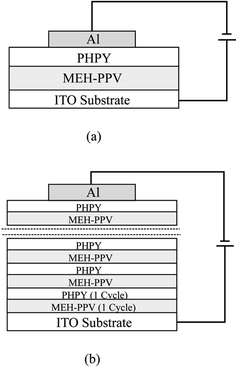 | ||
| Fig. 2 Schematic structures of (a) MEH-PPV–PHPY dual-layer device and (b) device comprising MEH-PPV (1 LB cycle) alternated with PHPY (1 LB cycle). | ||
Electrical and opto-electrical measurements were undertaken in a vacuum chamber. D.C. biases were supplied by a Farnell type C2 stabilised voltage supply and currents were measured using a Keithey 414A picoammeter. Impedance spectroscopy measurements were performed with a Hewlett Packard 4192 impedance analyser.15 The amplitude of the a.c. signal voltage was 70 mV rms. Spectra of 51 points, logarithmically spaced in the frequency range 5 Hz to 13 MHz, were obtained. For the electrical measurements reported below, ‘forward bias' is defined as a positive voltage applied to the ITO electrode.
The EL devices were mounted over a large area silicon photodiode detector. The light output was transmitted through the ITO electrode, the glass substrate and the glass window of the diode package onto the surface of the photodiode and the photocurrent generated was recorded using a Keithley 485 digital picoammeter. For external quantum efficiency measurements, the light power was calculated with a typical conversion factor of 0.31 A W−1 at 590 nm for the photodiode.
3. Results and discussion
The current versus voltage characteristics were found to depend strongly on the history of the device. In agreement with our previous results and those of other workers, peaks in the current were noted on the first voltage scan.13,16 However, these disappeared after two or three measurement cycles. All the electrical and opto-electrical data shown below were taken after the third voltage scan, after which reproducible characteristics had been obtained.The current and light output versus voltage curves for the ITO/MEH-PPV/Al devices (50 LB deposition cycles; polymer thickness 212 nm) for both forward and reverse biases are shown in Fig. 3; the inset shows the same data plotted on a logarithmic current scale. A distinct change of slope in the log (forward current) versus voltage plot is evident at approximately 15 V. This forward characteristic was reproducible from one device to the next. However, the magnitude of the reverse current varied between devices fabricated under seemingly identical conditions.
 | ||
| Fig. 3 Current and light output versus voltage characteristics for MEH-PPV single layer device (50 LB cycles; thickness 212 nm). The inset shows the logarithm (current) and the logarithm (light output) versus voltage characteristics. | ||
In forward bias, orange-yellow light was visible by eye in a darkened room. Weak light emission (also orange-yellow) was also noted from some devices in reverse bias. Fig. 4 contrasts the forward bias current versus voltage and light output versus voltage characteristics of the single layer and dual-layer LEDs. The latter device consisted of 10 LB deposition cycles of PHPY deposited on top of 30 LB cycles of MEH-PPV; the total organic film thickness was 190 nm. The forward currents measured for the two structures are similar. However, the light output for the dual-layer device is about one order magnitude higher than for single layer device, indicating correspondingly higher external quantum efficiency. Light output versus current density data for both devices are shown in Fig. 5(a) and the external quantum efficiency (photons out divided by electrons in) is plotted versus current density in Fig. 5(b). For high currents, the light output is approximately proportional to current density, resulting in a constant quantum efficiency. The saturated quantum efficiency is 7.5 × 10⁻³% for the dual-layer device and 5.7 × 10⁻⁴% for the single layer device.
 | ||
| Fig. 4 Comparison of the current versus voltage and light output versus voltage characteristics (both measured in forward bias) for a single layer MEH-PPV device (50 LB cycles, thickness 212 nm) and a dual-layer MEH-PPV (30 LB cycles)/PHPY (10 LB cycles) (total thickness 190 nm) structure. | ||
 | ||
| Fig. 5 (a) Light output and (b) external quantum efficiency versus current density characteristics for a MEH-PPV single layer device and a MEH-PPV/PHPY dual-layer structure. | ||
Fig. 6(a) shows the normalised photoluminescence spectrum obtained from films of 10 LB cycles of PHPY and 30 LB cycles of MEH-PPV. The electroluminescence spectra of both the single layer and dual-layer device under forward bias are compared in Fig. 6(b). In the case of the single layer device, the EL maximum (591 nm) coincides with that of the PL peak; there is also a shoulder around 625 nm in the EL spectrum. The EL spectrum of the dual-layer device is similar to that of the single layer MEH-PPV device, confirming that light emission originates from the MEH-PPV layer.
 | ||
| Fig. 6 (a) Normalised PL intensity for MEH-PPV (30 LB cycles) and PHPY (10 LB cycles). (b) Normalised EL intensity for MEH-PPV (50 LB cycles) single layer device and MEH-PPV (30 LB cycles)/PHPY (10 LB cycles) dual-layer structure. | ||
The higher external quantum efficiency for the dual-layer device can be explained by considering the charge transport characteristics and electronic band structures of the two organic materials. Pyridine-based polymers are well known as electron transporting materials whereas MEH-PPV is a good hole conductor. The energy band structure of the ITO/MEH-PPV/PHPY/Al structure is shown in Fig. 7 (the energy bands for PHPY are assumed to be similar to those of poly(pyridine-2,5-diyl)).10,11 The HOMO (highest occupied molecular orbital) level for MEH-PPV is close to the ITO Fermi level and, in forward bias, holes are easily transferred from the ITO to the polymer. The potential barrier to electrons from the Al top electrode to the PHPY layer is about 0.8 eV, considerably less than the barrier from Al to MEH-PPV (1.4 eV) in a single layer device. At the MEH-PPV/PHPY interface there is a barrier of 0.6 eV for electrons and 1.4 eV to holes. Consequently, electrons are transferred relatively easily between the PHPY and MEH-PPV, while holes are blocked and accumulate in the MEH-PPV layer, i.e. at the interface between the two polymers. Hence carrier recombination in the dual-layer device takes place in the MEH-PPV layer, explaining why the electroluminescence spectrum is characteristic of this polymer. The dual-layer structure both enhances the probability of charge capture recombination and separates the emission zone from the Al electrode, avoiding nonradiative quenching effects.
 | ||
| Fig. 7 Potential energy diagram for an ITO/MEH-PPV/PHPY/Al structure. | ||
In our experiments on spin-coated dual-layer devices it was found that the ratio of the thickness of the polymer layers could be used to optimise the LED efficiency.10,11 The efficiencies of the LB film MEH-PPV/PHPY dual-layer devices are compared in Table 1. The external quantum efficiency of the MEH-PPV (50 LB cycles)/PHPY(25 LB cycles) device is almost an order of magnitude less than that of the device discussed above. Presumably, if the polymer thicknesses are increased beyond certain values, the chance that carriers become trapped during their migration to the interface between the two organic layers is high.
| Device structure | Total thickness/nm | External quantum efficiency (%) |
|---|---|---|
| ITO/MEH-PPV (50)/Al | 212 | 6.0 × 10⁻⁴ |
| ITO/MEH-PPV (20)/PHPY (10)/Al | 136 | 4.3 × 10⁻³ |
| ITO/MEH-PPV (30)/PHPY (10)/Al | 190 | 7.5 × 10⁻³ |
| ITO/MEH-PPV (30)/PHPY (15)/Al | 204 | 4.7 × 10⁻³ |
| ITO/MEH-PPV (50)/PHPY (25)/Al | 263 | 8.0 × 10⁻⁴ |
| ITO/30 cycles of MEH-PPV (1) and PHPY (1)/Al | 192 | 1.0 × 10⁻⁴ |
The current through the alternate-layer system was found to be one order of magnitude lower than that for the MEH-PPV (30 cycles)–PHPY (10 cycles) dual-layer system even though total film thickness is similar (data not shown). Table 1 reveals very low quantum efficiency for the alternate-layer device. Such a structure will contain many potential barriers (due to MEH-PPV/PHPY interfaces) that the carriers will have to overcome. Effects due to the confinement of carriers in these multiple quantum wells were not apparent in this study.
Fig. 8 shows the forward bias impedance (Z) results for a single layer LED (Fig. 8(a)) and a dual-layer structure (Fig. 8(b)) in the form of Cole–Cole plots (Im (Z) versus Re (Z)). Such plots provide an insight into the electrical equivalent circuit of a device. In the graphs, the frequency increases from right to left (5 Hz to 13 MHz) around the semicircles. The data for the single layer device exhibit a series of semicircles, the diameter of which decreases with increasing forward bias. Close inspection (not evident from the scale of Fig. 8(a)) reveals that the high frequency intercept of the semicircle with the abscissa is about 100 Ω for all values of the applied forward voltage. This is the result of a small series resistance RS associated with the ITO contact and lead resistances. The Cole–Cole plots are similar to those reported in the literature for single layer LEDs based on MEH-PPV,17 PPV18,19 and PHPY.20 The LED structures can be modelled by a parallel resistance and capacitance combination, representing the dominant mechanisms of charge transport and polarisation in the organic layer, in series with a resistance representing the ITO contact.
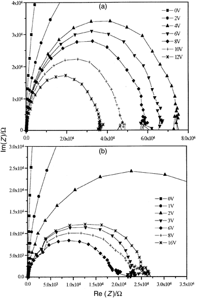 | ||
| Fig. 8 Imaginary versus real parts of the complex impedance Z for (a) MEH-PPV (50 LB cycles; thickness 212 nm) and (b) MEH-PPV (30 LB cycles)–PHPY (10 cycles) (total thickness 190 nm) dual-layer structure. Data are for forward bias. | ||
The Cole–Cole plot for the dual-layer structure, Fig. 8(b), is more complex. At least two semicircles are evident for d.c. voltages greater than about 3 V. The diameter of the ‘main' semicircle decreases with increasing voltage decreases until 6 V, the turn-on voltage for EL; at higher biases the diameter increases. For some of the dual-layer devices studied, the diameter of this semicircle decreased at higher forward voltages. These effects are related to maxima in the capacitance versus voltage and conductance versus voltage curves (data not shown). In contrast, the high frequency semicircle (on the left in Fig. 8(b)) is relatively unaffected by bias and is displaced, by approximately 100 Ω, along the Re (Z) axis.
Two semicircles (originating from two parallel resistor/capacitor combinations connected in series) are often observed in organic LEDs when the polymeric layer is ‘thick'.15,18,21,22 One of these RC circuits is thought to represent a Schottky barrier while the other models the capacitance and resistance of a neutral bulk region in the polymer film. However, this explanation does not fit with our results, as the single layer and dual-layer devices are of similar thickness. It is more likely that at least one of the Cole–Cole semicircles in Fig. 8(b) is associated with the additional interface in the dual-layer device. The unusual voltage dependence of both the capacitance and conductance may be due to an admittance contribution from traps at the MEH-PPV/PHPY interface. Similar phenomena are well-known for inorganic semiconductor/insulator junctions (e.g. Si/SiO2).23
The Cole–Cole plots in reverse bias for both the MEH-PPV and MEH-PPV/PHPY devices (data not shown) showed only a single semicircle, the diameter of which decreased as voltage increases. The series resistance was found to be the same as that determined by forward bias measurements. Over the range of voltage investigated, the diameter of semicircles in reverse bias was larger than that in forward bias, reflecting the higher resistance of the devices.
4. Conclusions
Multilayers of MEH-PPV and PHPY were deposited using the standard vertical dipping Langmuir–Blodgett technique. Orange-yellow light emission was observed when forward bias was applied to the MEH-PPV single layer device and an external quantum efficiency of 5.7 × 10⁻⁴% was measured. By using the electron transfer material, PHPY, between the MEH-PPV and the aluminium electrode, the efficiency increased to 7.5 × 10⁻³%, more than ten times higher than the single layer device. The EL spectrum of the dual-layer device is similar to that of the MEH-PPV single layer device, confirming that light emission originates from MEH-PPV layer. Impedance spectroscopy using the dual-layer structure revealed some unusual dependencies of the conductance and capacitance on applied voltage. This is currently the subject of further investigation.Acknowledgements
We would like to thank Aventis for supplying the MEH-PPV and the Engineering and Physical Sciences Research Council for the award of a ROPA grant. IDWS is a Royal Society Research Fellow.References
- J. H. Burroughes, D. D. C. Bradley, A. R. Brown, R. N. Marks, K. Mackay, R. H. Friend, P. L. Burn and A. B. Holmes, Nature, 1990, 347, 539 CrossRef CAS.
- D. D. C. Bradley, Synth. Met., 1993, 54, 401 CrossRef CAS.
- C. W. Tang and S. A. Vanslyke, Appl. Phys. Lett., 1987, 51, 913 CrossRef CAS; J. Kido, Phys. World, 1999, 12, 27 Search PubMed.
- A. J. Heeger, I. D. Parker and Y. Yang, Synth. Met., 1994, 67, 24 CrossRef CAS.
- M. I. Sluch, C. Pearson, M. C. Petty, M. Halim and I. D. W. Samuel, Synth. Met., 1998, 94, 285 CrossRef CAS.
- A. Bolognesi, C. Botta, G. Bajo, R. Österbacka, T. Östergård and H. Stubb, Synth. Met., 1998, 98, 123 CrossRef CAS.
- R. Österbacka, G. Juška, K. Arlauskas, A. J. Pal, K.-M. Källman and H. Stubb, J. Appl. Phys., 1998, 84, 3359 CrossRef CAS.
- R. Österbacka, A. J. Pal and H. Stubb, Thin Solid Films, 1998, 327–329, 668 CrossRef CAS.
- L. M. Goldenberg, M. Leclerc, A. Donat-Bouillud, C. Pearson and M. C. Petty, Thin Solid Films, 1998, 327–329, 715 CrossRef CAS.
- S. Dailey, M. Halim, I. D. W. Samuel and A. P. Monkman, Proc. SPIE Organic Light-Emitting Materials and Devices, San Diego, 1997, 3148, 82. Search PubMed.
- S. Dailey, M. Halim, E. Rebourt, L. E. Horsburgh, I. D. W. Samuel and A. P. Monkman, J. Phys: Condens. Matter, 1998, 10, 5171 Search PubMed.
- T. Yamomoto, T. Maruyama, Z. –H. Zhou, T. Ito, T. Fukuda, Y. Yoneda, F. Begum, T. Ikeda, S. Sasaki, H. Takezoe, A. Fukuda and K. Kubota, J. Am. Chem. Soc., 1994, 116, 4832 CrossRef CAS.
- C. Pearson, M. Kilitziraki, S. Dailey, L. E. Horsburgh, A. P. Monkman, I. D. W. Samuel and M. C. Petty, submitted to IEEE Trans. .
- J. C. Scott, J. H. Kaufman, P. J. Brock, R. Dipietro, J. Salem and J. A. Goitia, J. Appl. Phys., 1996, 79, 2745 CrossRef CAS.
- M. Meier, S. Karg and W. Riess, J. Appl. Phys., 1997, 82, 1961 CrossRef CAS.
- F. Garten, J. Vrijmoeth, A. R. Schlatmann, R. E. Gill, T. M. Klapwijk and G. Hadziioannou, Synth. Met., 1996, 76, 85 CrossRef CAS.
- I. H. Campbell, D. L. Smith and J. P. Ferraris, Appl. Phys. Lett., 1995, 66, 3030 CrossRef CAS.
- A. J. Campbell, D. D. C. Bradley and D. G. Lidzey, J. Appl. Phys., 1997, 82, 6326 CrossRef CAS.
- W. Bijnens, J. Manca, T. D. Wu, M. D'Olieslaeger, D. Vanderzande, J. Gelan, W. De Ceuninck, Luc De Schepper and L. M. Stals, Synth. Met., 1996, 83, 261 CrossRef CAS.
- S. Capaccioli, C. Pearson, A. P. Monkman, L. E. Horsburgh, P. A. Rolla and M. C. Petty, submitted to J. Phys. D..
- W. Riess, S Karg, V. Dyakonov, M. Meier and M. Schwoerer, J. Lumin., 1994, 60 & 61, 906.
- J. Scherbel, P. H. Nguyen, G. Paasch, W. Brutting and M. Schwoerer, J. Appl. Phys., 1998, 83, 5045 CrossRef CAS.
- E. H. Nicollian and J. R. Brews, MOS (Metal Oxide Semiconductor) Physics and Technology, Wiley-Interscience, New York, 1982. Search PubMed.
Footnote |
| † Basis of a presentation given at Materials Chemistry Discussion No. 2, 13–15 September 1999, University of Nottingham, UK. |
| This journal is © The Royal Society of Chemistry 2000 |