DOI:
10.1039/A903046H
(Paper)
J. Mater. Chem., 2000,
10, 27-30
Molecular beam deposition of crystalline layers of polar perhydrotriphenylene inclusion compounds characterised by second harmonic generation microscopy†
Received 16th April 1999, Accepted 1st June 1999
First published on UnassignedUnassigned22nd December 1999
Abstract
Polar inclusion compounds of perhydrotriphenylene (PHTP) were grown in nm to μm thick crystalline layers on glass and sapphire substrates. Nucleation was facilitated by using silanised glass. Second harmonic generation microscopy and confocal second harmonic generation microscopy were used to identify the deposition of polar PHTP–guest layers and to determine the growth direction. Channels formed by the inclusion compound were found to grow parallel to the glass substrate.
1. Introduction
Polar organic compounds have been grown as thin films by the Langmuir–Blodgett technique, molecular beam deposition and related means (for a review see Whitten et al.1). In cases of an acentric packing of chromophores in layers grown on amorphous or crystalline substrates, nonlinear optical (NLO)2 and electronic properties3 are of current interest. Except for some attempts in growing genuine epitaxial layers on organic substrates, most crystalline layers reported so far are of the van der Waals type. Following work by Koma et al.,4,5 lattice matching is not considered to be a critical prerequisite to deposit crystalline films if the layer and the substrate are mainly interacting through van der Waals forces (for a review see Koma6).In this paper we report for the first time on the thin layer growth of polar inclusion compounds of perhydrotriphenylene (PHTP) and NLO molecules, e.g.N,N-dimethyl-p-nitroaniline (DMNA) and 1-(4-nitrophenyl)piperazine (NPP). In the supramolecular architecture of PHTP channel-type inclusion compounds, six stacks of disk-shaped PHTP molecules include rod-shaped guest molecules such as DMNA or NPP.7 In bulk crystals a bipolar state is formed, where uniform polarisation within cone-shaped macrodomains originates from a Markov-type attachment process during growth along the channel direction.8,9
Provided that E(-NO2···O2N-)≠E(-N(CH3)2···(CH3)2N-) for DMNA, and E(-NO2···O2N-)≠E(-NH···HN-) for NPP (E = attachment energies for functional groups), macrodomains are polar.10 The crystal structure of the guest DMNA itself is acentric,11 although an almost antiparallel packing of dipoles cancels most of the macroscopic nonlinearity given by the molecular hyperpolarisability βzzz along the charge transfer axis of DMNA. For the second guest material, no crystal data are yet available. However, frequency doubling experiments with NPP crystallites showed no nonlinear optical activity.12 Using second harmonic generation (SHG) in the course of identifying the polar state of layers of PHTP–guest inclusion compounds, we can assume the detection of only weak or almost negligible SH responses13 originating from possible codeposits of either of the pure guest materials (no polymorphs known for DMNA, NPP). Because of polar chain formation of guest molecules in adjacent channels, PHTP–guest systems grown in thin layers represent interesting systems for the study of photoinduced charge migration along polar chains in well separated channels. Evidence for molecular rectifier properties of PHTP–guest bulk crystals has been reported recently.14 However, bulk crystals do not allow low current measurements at electrical fields of ∼ 108 V m−1 or higher, necessary to observe typical diode characteristics in the current-voltage curves. If we had the means to obtain crystalline layers grown between electrodes at a distance d
≤ 10 μm, characterisation may be more feasible by applying voltages compatible with present ammeters. For this purpose we have started to grow layers of PHTP–guest materials on various substrates. Thereby, a primary step of characterisation was to demonstrate (i) the deposition of a polar PHTP–guest phase and (ii) to determine the growth direction of layers with respect to the substrate plane. To investigate the polar packing of guests in layers of PHTP inclusion compounds we have imaged the optical nonlinearity of crystallites by (confocal) second harmonic generation microscopy (SHGM15 and cSHGM16).
2. Experimental
PHTP and guest compounds were evaporated from separate Knudsen cells attached to a custom-made vacuum chamber. Both Knudsen cells were separated by mechanical shutters from the growth chamber. The molecular beams met the substrate surface at 45°. A thermostat stabilised the substrate temperature, measured near the substrate. The cell temperatures Tcell around 100![[thin space (1/6-em)]](https://www.rsc.org/images/entities/char_2009.gif) °C were kept below the melting points mp of the compounds (mpPHTP = 125°C, mpDMNA = 163°C, mpNPP = 132°C). Therefore, the compounds sublimed from the solid phase. Under these conditions, a contamination of the deposit with decomposition products is unlikely. The vapour pressure p of DMNA is known (p=exp(A−B/T) in Pa, A = 32.245 (±0.05), B = 11624 (±220) K17), whereas the A, B parameters of PHTP are under investigation.18 From the vapour pressure, a calculated flux of 1015 s−1 cm−2 results for DMNA. In the PHTP–DMNA experiments, we observed resublimation of the compounds at the cell orifices caused by temperature gradients in the cells. Therefore, the experimental DMNA flux is probably lower than the theoretical prediction. In the PHTP–NPP experiments, the flux of PHTP was in the region of 1015 s−1 cm−2 (determined from the mass losses). This is higher by a factor of 10 than the flux of the guest NPP.
°C were kept below the melting points mp of the compounds (mpPHTP = 125°C, mpDMNA = 163°C, mpNPP = 132°C). Therefore, the compounds sublimed from the solid phase. Under these conditions, a contamination of the deposit with decomposition products is unlikely. The vapour pressure p of DMNA is known (p=exp(A−B/T) in Pa, A = 32.245 (±0.05), B = 11624 (±220) K17), whereas the A, B parameters of PHTP are under investigation.18 From the vapour pressure, a calculated flux of 1015 s−1 cm−2 results for DMNA. In the PHTP–DMNA experiments, we observed resublimation of the compounds at the cell orifices caused by temperature gradients in the cells. Therefore, the experimental DMNA flux is probably lower than the theoretical prediction. In the PHTP–NPP experiments, the flux of PHTP was in the region of 1015 s−1 cm−2 (determined from the mass losses). This is higher by a factor of 10 than the flux of the guest NPP.With shutters closed, the cleaned substrates were annealed for 1 h at a temperature Ta (annealing temperature) to remove adsorbed water from its surface. Sapphire crystal plates (75° to c-axis) were purified for 1 h in sulfuric acid and washed in doubly distilled water. The glass substrates were passively silanised by dipping them for 30 min into a toluene solution of a silicon oil (Dow Corning 200) at ∼50°C. The silanised glass substrates were dried at ∼270°C for 2 h. Substrates featuring a glass as well as a silanised surface were produced by dipping one half of the silanised substrate for 1 h into concentrated sulfuric acid. The partially silanised glass substrates were washed in doubly distilled water and absolute ethanol (analytical grade). After cooling the substrate to Ts = 0°C (substrate temperature), a base pressure of 5 × 10⁻⁷ hPa was reached. Thereafter, the shutters were opened and deposition was carried out at cell temperatures Tcell, Ts = 0°C and a deposition pressure of 10−6 hPa. Because a starting value of Ts = 0°C did not induce nucleation, Ts was lowered to the growth temperature Tg. After a certain growth time tg the shutters were closed and the chamber was filled with argon (1 bar), while Tg was increased to room temperature within 2 h. All growth parameters are summarised in Table 1. Obtained films were characterised ex situ by optical microscopy (LEITZ DM RXP in transmission), atomic force microscopy (AFM, Park Scientific Instruments, Autoprobe CP) and (confocal) second harmonic generation microscopy (SHGM and cSHGM). For SHGM, we used a pulsed Nd:YAG laser (λ = 1064 nm) in addition to the illumination in transmission. Absorbing the fundamental light with a IR blocking filter, a superposition of the green SH light with the optical image is detected by a CCD camera. In the confocal geometry, the focus of a picosecond Ti:sapphire laser (λ = 790 nm) was scanned over the sample. The SH light was separated with an interference filter and measured with an avalanche photodiode and a photon counter.
Table 1 Growth parameters for PHTP–DMNA and PHTP–NPP
| Growth parameters | PHTP–DMNA | PHTP–NPP |
|---|
| Substrate | (a): sapphire | (b): silanised glass | glass, partially silanised |
| Annealing temperature Ta | (a): 300°C | (b): 100°C | 100°C |
| Cell temperature Tcell | PHTP, DMNA: 100°C | PHTP: 110°C, NPP: 120°C |
| Cell orifice diameter dcell | (a): 300 μm | (b): 100 μm | 100 μm |
| Growth temperature Tg | (a): −3°C | (b): −20°C | (a): −15°C | (b): −20°C |
| Growth time tg | 3 days | 24 h |
3. Results and discussion
PHTP–DMNA
(a) Tg = −3![[thin space (1/6-em)]](https://www.rsc.org/images/entities/b_char_2009.gif) °C. As a result of different runs, the sapphire surface (diameter ∼9 mm) was mainly covered by a thin deposition. Crystallites were up to ∼2–4 μm wide and grew to heights of ∼30–70 nm, as measured by AFM (Fig. 1). Using the contact mode, imaged features remained mechanically stable. In between this rather homogeneous coverage we observed larger crystallites showing a needle type morphology (up to some 10 μm long) developing a height of ∼1 μm. If observed at ambient conditions, deposition features were surprisingly stable over a few weeks.
°C. As a result of different runs, the sapphire surface (diameter ∼9 mm) was mainly covered by a thin deposition. Crystallites were up to ∼2–4 μm wide and grew to heights of ∼30–70 nm, as measured by AFM (Fig. 1). Using the contact mode, imaged features remained mechanically stable. In between this rather homogeneous coverage we observed larger crystallites showing a needle type morphology (up to some 10 μm long) developing a height of ∼1 μm. If observed at ambient conditions, deposition features were surprisingly stable over a few weeks. |
| | Fig. 1 AFM image (contact mode) of the PHTP–DMNA deposition on sapphire. The heights of the crystallites are ∼70 nm in profile (A) and ∼130 nm in profile (B). | |
Following the results of a gas chromatographic analysis, these films contained much more PHTP than expected for a (PHTP)4.4DMNA compound. Probably, they represent intergrowth of PHTP and inclusion crystals. At a large excess of PHTP it is unlikely that pure DMNA crystals are deposited. In all other types of crystal growth experiments (melt, solution, gas) (PHTP)4.4DMNA formed easily. Confirmation of the crystallinity by means of polarisation microscopy, 2θ X-ray scans and transmission electron microscopy was not possible. Also SHG microscopy was not sensitive enough to detect the nonlinearity of these nm thick films. However, a scanning confocal SHG microscopy technique, providing a lateral resolution of ∼1 μm, could reveal a nonlinear optical response (Fig. 2). A quite homogeneous distribution of SH intensity has been observed over certain crystallites (white regions). Other domains featured an inhomogeneous distribution of SH response (grey). The substrate itself showed low SH background (black surrounding). In Fig. 2 the fundamental light was unpolarised. In this case no information on the orientation of the polar axis could be obtained.
 |
| | Fig. 2 SH response of the PHTP–DMNA deposition on sapphire imaged by cSHGM. White regions represent crystallites revealing strong and homogeneous distributions of generated SH light, grey indicates inhomogeneous distribution of SH intensity over domains. The black surroundings are bare non-SHG active sapphire substrate. | |
(b) Tg = −20°C. On silanised glass substrates, needle shaped crystallites grew into lengths of 50–100 μm and heights up to ∼ 15 μm. Some of them were assembled parallel, whereas others were arranged in star-shaped formations. Due to the increase of thickness by lowering the growth temperature, the SH intensity was strong enough to be detected by the SHG microscope. The superposition of the optical image (blue) and the green SH response in transmission is shown in Fig. 3. The dependence of the SH signal on the polarisation E of the fundamental light indicates that the dipole axis of DMNA is in-plane with the substrate. Because of the large excess of PHTP at a cell temperature of 100°C, it is unlikely that the needles consisted of pure DMNA. In a control experiment using the same growth conditions—but with closed shutter for PHTP—no detectable amounts of DMNA could be deposited. Therefore we conclude, that the needle-shaped crystallites were composed of PHTP–DMNA inclusion compound. The needle axis can be identified as the main growth direction in bulk crystals, which is parallel to the channels.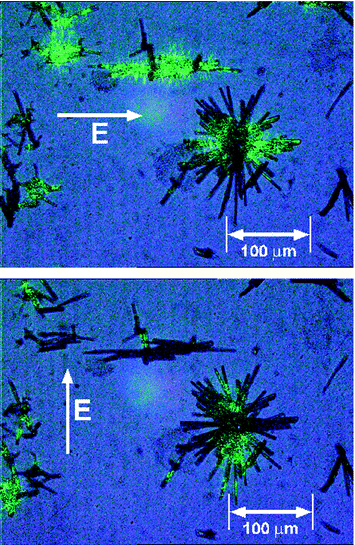 |
| | Fig. 3 Superposition of the optical image (blue) and the SH response (green) in transmission of PHTP–DMNA needles at Tg = −20°C. A strong dependence of the SH intensity on the polarisation E of the fundamental light is observable. | |
PHTP–NPP
(a) Tg = −15°C. At relatively high growth temperatures of Tg
≥
−15°C, the silanised part of the glass substrate was weakly but homogeneously covered by dendritic features of diameters up to 100 μm. Visible with the SHG microscope, the dendritic crystallites exhibited a strong nonlinear optical activity, which suggests that the deposition mainly consisted of the PHTP–NPP inclusion compound. Fig. 4 shows a superposition of the optical image and the SH response (white regions) in transmission. The dependence of the SH signal on the polarisation E of the fundamental light indicates that the channel axis c is in-plane with the substrate. Furthermore, the c-axis corresponds to the main growth direction of the dendritic arms. This is in agreement with the observations that c is the preferred growth direction in macroscopic needle-shaped PHTP–NPP crystals, grown in the gas phase or from solution. |
| | Fig. 4 Superposition of the optical image (grey) and the SH response (white regions) in transmission of the weak PHTP–NPP coverage at Tg = −15°C. The dependence of the SH intensity on the polarisation E of the fundamental light is clearly visible. | |
(b) Tg = −20°C. At lower growth temperatures Tg
≤
−20°C the coverage showed a strong dependence on the substrate. On the non-silanised part the coverage was almost negligible, whereas almost full coverage was observed on the silanised side. The deposition consisted of star-shaped features with crystalline needle-like domains. The typical length of these needles was 20–30 μm at a width of 4–10 μm and a height of 2 μm. In the fully covered (silanised) region the crystallites started to overlap. Superposition of the optical image (blue) and the green SH response of an area with a medium coverage level are shown in Fig. 5. Needles oriented parallel to the polarisation direction E of the fundamental light led to the maximum SH responses, leading to the conclusion that the needle-shaped crystallites are mainly PHTP–NPP inclusions. As found for smaller deposits, the channel axis is in-plane with the substrate. SHG inactive regions of the deposit may consist of pure PHTP which was sublimed in excess. Another reason for a non-detectable or an inhomogeneous distribution of the SH intensity could be a thickness variation of the deposit. The SH intensity is proportional to the square of the thickness of a SHG active material. Under ambient conditions the deposited crystallites were stable for at least some days. By a control experiment using the same growth parameters as for PHTP–NPP—but without opening the shutter of the PHTP cell—we have deposited NPP crystallites showing no detectable SH signal. Therefore, the SHG activity and its polarisation dependence provide evidence for the existence of PHTP–NPP inclusion compound grown in layers. |
| | Fig. 5 Superposition of the optical image (blue) and the SH response (green) in transmission of the medium PHTP–NPP coverage at Tg = −20°C. The crystalline needles parallel to the polarisation direction E of the fundamental light showed maximum SH intensity. | |
4. Conclusions and outlook
For the first time, molecular beam deposition using a double source evaporation technique for the host PHTP and guests led to crystalline layers which consisted of PHTP inclusion compounds. The coverage level could be changed by a variation of the substrate material and the growth temperature. Application of polarised SHG microscopy showed that the channel axis c of the supramolecular architecture is oriented parallel to the substrate. In bulk crystals grown from the gas phase or solution this corresponds to the fast-growing direction. The in-plane growth of c is of interest to further experiments, where we will introduce planar electrodes to obtain thin film growth between them. Such a configuration may allow the application of electrical fields large enough to measure a significant effect of electrical rectification. Another application may be the use of n- and p-type electrodes to favour electroluminescence from a charge carrier recombination in individual channels of PHTP-guest compounds. Experiments along these lines are in progress.Acknowledgements
This work received support from the NFP 36 project [Nanoscience (4036-0439932)], the ‘Hochschulstiftung' (Wander, University of Berne) and from the ‘Stipendienfonds der Basler Chemischen Industrie'.References
- D. G. Whitten, T. Kajiyama and T. Kunitake, MRS Bulletin, 1995, June, 18 Search PubMed.
- R. Schlesser, T. Dietrich, Z. Sitar and P. Günter, Mater. Res. Soc. Symp. Proc., 1996, 413, 179 Search PubMed.
- Molecular Electronics, ed. J. Jortner and M. Ratner, Blackwell Science Ltd, Oxford, 1997. Search PubMed.
- A. Koma, K. Sunouchi and T. Miyajima, Microelectron. Eng., 1984, 2, 129 CrossRef CAS.
- A. Koma, K. Sunouchi and T. Miyajima, J. Vac. Sci. Technol., 1985, B3, 724 Search PubMed.
- A. Koma, Prog. Cryst. Growth Charact., 1995, 30, 129 Search PubMed.
- J. Hulliger, O. König and R. Hoss, Adv. Mater., 1995, 7, 719 CAS.
- J. Hulliger, A. Quintel, M. Wübbenhorst, P. J. Langley, S. W. Roth and P. Rechsteiner, Opt. Mater., 1998, 9, 259 CrossRef CAS.
- J. Hulliger, P. Rogin, A. Quintel, P. Rechsteiner, O. König and M. Wübbenhorst, Adv. Mater., 1997, 9, 677 CAS.
- J. Hulliger, P. J. Langley, O. König, S. W. Roth, A. Quintel and P. Rechsteiner, Pure Appl. Opt., 1998, 7, 221 CrossRef CAS.
- T. C. Mak and J. Trotter, Acta Crystallogr., 1965, 18, 68 CrossRef CAS.
- R. Hoss, O. König, V. Kramer-Hoss, U. Berger, P. Rogin and J. Hulliger, Angew. Chem., Int. Ed. Engl., 1996, 35, 1664 CrossRef CAS.
- J. Hulliger, Z. Kristallogr., 1998, 213, 441 Search PubMed.
- A. Quintel and J. Hulliger, Synth. Met., 1999, in press. Search PubMed.
- M. Flörsheimer, H. Salmen, M. Bosch, C. Brillert, M. Wierschem and H. Fuchs, Adv. Mater., 1997, 9, 1056 CrossRef CAS.
- J. Vydra and M. Eich, Appl. Phys. Lett., 1998, 72, 275 CrossRef CAS.
- W. E. Acree, S. A. Tucker, G. Pilcher and G. Toole, J. Chem. Thermodyn., 1994, 26, 85 CrossRef CAS.
- F. Budde and J. Hulliger, to be published. .
Footnote |
| † Basis of a presentation given at Materials Chemistry Discussion No. 2, 13–15 September 1999, University of Nottingham, UK. |
|
| This journal is © The Royal Society of Chemistry 2000 |
Click here to see how this site uses Cookies. View our privacy policy here.