Organic materials for electronic and optoelectronic devices†
Yasuhiko Shirota
Department of Applied Chemistry, Faculty of Engineering, Osaka University, Yamadaoka, Suita, Osaka, 565-0871, Japan. E-mail: shirota@ap.chem.eng.osaka-u.ac.jp
First published on UnassignedUnassigned4th April 2000
Abstract
This article concentrates on our recent results on several classes of photo- and electro-active organic materials that permit thin film formation and discusses their synthesis, properties, functions and potential applications for electronic and optoelectronic devices. The materials studied include amorphous molecular materials, titanyl phthalocyanine, oligothiophenes with well-defined structures, and non-conjugated polymers containing pendant oligothiophenes or other π-electron systems. The thin films of these materials find potential applications for use in organic electroluminescent, photovoltaic, electrochromic, and other devices.
1 Introduction
Recent extensive studies have shown that organic materials exhibit a variety of interesting optical, electrical, photoelectric, and magnetic properties in the solid state. Photo- and electro-active organic materials have been the subject of recent attention, including organic semiconductors, organic metals including superconductors, organic photoconductors, organic photoactive materials for solar cells, organic non-linear optical materials, organic ferromagnets, photo- and electrochromic organic materials, resist materials, liquid crystals, and others. Among them, organic photoconductors, liquid crystals, and resist materials have been put to practical use for photoreceptors in electrophotography, display devices, and lithographic processes for the production of semiconductor devices. In addition, organic materials have found a number of potential applications for use in electronic and optoelectronic devices such as sensors, plastic batteries, solar cells, field-effect transistors, optical data storage, organic electroluminescent devices, switching devices, frequency doublers, and many others.In contrast to inorganic materials that consist of covalent or ionic bonds of atoms over the entire expanse of solids, organic materials are based on independent molecules and characterised by weak intermolecular interactions. Therefore, designs of organic materials can be readily performed on the molecular level. In particular, organic π-electron systems have received attention as potential photo- and electro-active materials. When these organic materials are used in electronic and optoelectronic devices, they are normally in the form of thin films. Organic thin films are prepared by various techniques, e.g., solvent cast from solution, spin coating, vacuum vapor deposition, electrochemical deposition, Langmuir–Blodgett and monolayer self-assembly techniques. Both ordered and disordered films can be generated, depending on the technique of thin film fabrication.
We have performed studies of the creation of novel photo- and electro-active organic materials and their structures, reactions, properties, functions and applications for electronic and optoelectronic devices. This article concentrates on our recent results on several classes of organic materials that permit thin film formation, e.g., amorphous molecular materials, titanyl phthalocyanines, oligothiophenes with well-defined structures, and non-;conjugated polymers containing pendant oligothiophenes or other π-electron systems, and discusses their synthesis, structures, reactions, properties, functions, and potential applications for electronic and optoelectronic devices. Amorphous molecular materials have found successful application for use in organic electroluminescent (EL) devices and are expected to find further potential applications as photovoltaic, photochromic and resist materials. Photovoltaic devices using titanyl phthalocyanine, oligothiophenes with well-defined structures, and pendant polymers and electrochromic devices using a novel family of polymers containing pendant oligothiophenes have been studied. General aspects of these devices are briefly described here.
Organic electroluminescent (EL) devices
Organic EL devices have recently received a great deal of attention for their application as full-colour, flat-panel displays as well as from the standpoint of scientific interest. They are attractive because of low voltage driving, high brightness, capability of multicolour emission by the selection of emitting materials and easy fabrication of large-area and thin-film devices. Following the reports on organic EL devices using single crystals of anthracene,1 recent pioneering works on organic EL devices using low molecular-weight organic materials2 and a conjugated polymer3 have triggered extensive research and development of this field.The structure of organic EL devices consists of single or multiple layers of organic thin films sandwiched normally between the transparent indium-tin-oxide (ITO) coated glass and vacuum-evaporated metals with low work function such as magnesium (Mg) and aluminium (Al). The operation of organic EL devices involves injection of holes and electrons from the ITO and Mg or Al electrodes, respectively, transport of injected charge carriers, recombination of holes and electrons in the emission layer to generate an electronically excited state molecule, followed by luminescence emission. In order to achieve high performance in organic EL devices, it is necessary to attain charge balance. Generally, layered devices consisting of charge-transport and emitting layers can more readily achieve charge balance than single-layer devices using an emitting material alone. This is because a suitable combination of charge-transporting and emitting materials in layered devices reduces the energy barrier for the injection of charge carriers from the electrodes and because the charge-transport layer acts as a blocking layer against the injection of either holes or electrons from the adjoining layer and their subsequent escape from the device.
For the fabrication of high-performance organic EL devices, not only emitting materials but also charge-transporting materials are required. Both polymers and small molecules are candidates for materials in organic EL devices. The materials for organic EL devices should meet the following requirements: (1) to possess a suitable ionisation potential and electron affinity for energy level matching for the injection of charge carriers at the interfaces between the electrode/organic material and organic material/organic material, (2) to permit the formation of a uniform film without pinholes, (3) to be morphologically stable, (4) to be thermally stable, (5) to be electrochemically stable, and (6) to be highly luminescent for emitting materials. In addition, doping of luminescent compounds has been shown to be an effective method for attaining high brightness and desirable emission colour.4
For the fabrication of high-performance organic EL devices, development of new materials with high performance and judicious choice of the combination of emitting and charge-transporting materials and the combination of emitting and luminescent dopant molecules as well as an understanding of basic processes, such as charge injection from the electrodes, charge transport, recombination of charge carriers to generate the electronically excited-state molecule, are of vital importance.
Recent years have witnessed significant progress with regard to brightness, multi- or full-colour emission, and durability and thermal stability of organic EL devices.
Organic photovoltaic devices
Devices for photoelectric conversion using organic materials, which find potential applications as solar cells and photosensors, are mainly classified into photoelectrochemical and photovoltaic devices. Photoelectrochemical cells consist of inorganic semiconductors and organic dyes as a sensitiser immersed in an ionically conductive electrolyte containing a redox couple, where light is absorbed by the organic dye.5,6 Photovoltaic devices consist of thin films of organic materials sandwiched between two metal electrodes. A built-in electric field, formed in the semiconductor in contact with the electrolyte in the photoelectrochemical cell and in the organic layer at the interface with the metal electrode or with the other organic layer in the photovoltaic device, is responsible for the photogeneration of charge carriers.Organic solid-state photovoltaic devices have attracted attention because of their light weight, potentially low cost, and ready fabrication of large-area, thin-film devices. Both Schottky-type and p–n heterojunction cells using low molecular-weight organic materials and polymers have been fabricated, and their performance characteristics investigated. In Schottky-type cells, a single-layer organic material is sandwiched between two dissimilar electrodes to form a Schottky barrier in the organic layer at the interface with the metal electrode. On the other hand, p–n heterojunction cells are typically based on a double-layer structure of organic thin films, where the organic/organic interface plays an important role in the performance, the electrodes simply providing ohmic contacts to the organic layers. p–n Heterojunction devices have advantages over Schottky-type devices in that they do not necessarily need the use of low work-function metals that readily undergo air oxidation as electrode materials. It is also expected that a higher quantum yield for photogeneration of charge carriers is attained due to electron donor–acceptor interactions of the two dyes.
The conversion efficiency of organic photovoltaic devices is still lower than that of inorganic photovoltaic devices. The reason for this may be attributed to low photogeneration efficiency of charge carriers and to high electrical resistivity of organic materials which stems from the low mobility and low density of free carriers. The basic processes of the operation of organic photovoltaic devices have been understood in terms of the energy band model for inorganic semiconductors; however, many organic materials do not form energy bands. It is therefore necessary to understand the mechanism of photoelectric conversion in organic photovoltaic devices on the molecular level. It is important to understand what impurity species are involved in the formation of the built-in potential at the interface between the organic material and electrode and two kinds of organic materials as well as the mechanism for the photogeneration of charge carriers in organic materials. Improving the quantum efficiency of the photogeneration of charge carriers is a key issue for the development of organic photovoltaic devices with high conversion efficiency.
Recent significant progress in solid-state solar cells using the combination of organic dyes and inorganic semiconductors7 and using interpenetrating polymer networks8–10 has attracted renewed interest in this field.
Electrochromic devices
Organic electrochromic devices, which are characterised by low-voltage operation, good optical contrast, and wide viewing angle, can be potentially used as smart windows that control the sun radiation in buildings and cars, rear-view mirrors for cars, and display devices.11 Low molecular-weight organic compounds, e.g., viologen derivatives and metallophthalocyanines, and polymers including both π-conjugated and pendant polymers have been studied for electrochromic materials. Such organic materials have the potential capability of multi-colour display and in particular, polymer thin films are attractive because they may exhibit a memory effect and have a good cycle life. Improvement in the cyclability of the colouration and decolouration and the design and synthesis of new redox systems are important issues.12,13 All solid-state devices using polymer electrolytes or polymer gel electrolytes14,15 as well as electrochromic devices using thin films of organic materials immersed in an electrolyte solution have been studied. Photoinduced electrochromic devices have also been studied.162 Amorphous molecular materials
Low molecular-weight organic compounds generally tend to crystallise readily, and hence they usually exist as crystals below their melting points, except for certain solvents, e.g., 2-methyltetrahydrofuran, which readily form glasses at 77 K. Although it had been reported that amorphous or quasi-amorphous films of polycyclic aromatic hydrocarbons are formed by vacuum deposition at low temperature17 and a few organic compounds form amorphous glasses at ambient temperatures,18,19 little attention had been paid to amorphous glasses of low molecular-weight organic compounds until the late 1980s.Since then, we have performed systematic studies of the creation of low molecular-weight organic compounds that readily form stable amorphous glasses above room temperature, which we refer to as “amorphous molecular materials" or “molecular glasses", and their structures, reactions, properties, functions and applications. We considered that such work may open up a new field of organic materials science that deals with molecular glasses as distinct from covalently-bonded inorganic glasses and that such amorphous molecular materials may constitute a new class of organic functional materials.
Amorphous molecular materials or molecular glasses are of interest because of the following aspects. They are in a thermodynamically nonequilibrium state and hence may exhibit glass-transition phenomena usually associated with amorphous polymers. It is thought that they assume a variety of states such as the amorphous glass, supercooled liquid, and crystal. They may be characterised by the presence of free volume and by the disorder of both intermolecular distance and orientation. They may form uniform, transparent amorphous thin films by vapor deposition and spin-coating methods. In contrast to single crystals and liquid crystals which show anisotropic properties, amorphous molecular materials may exhibit isotropic properties as well as homogeneous properties due to the absence of grain boundaries. In contrast to polymers, they are pure materials with well-defined molecular structures and definite molecular weights without any distribution. We have been interested in elucidating the correlation between molecular structure and glass-forming properties, structures of molecular glasses, relaxation processes of molecular glasses, reactions in molecular glasses as a new medium, properties of molecular glasses, dynamic control of properties and functions, and applications of amorphous molecular materials for electronic and optoelectronic devices.
In this section, amorphous molecular materials are discussed from the following three standpoints: (1) design and synthesis of amorphous molecular materials, (2) characteristic features of their structures, reactions, and properties, and (3) functions and applications of amorphous molecular materials.
2.1 Design and synthesis of amorphous molecular materials
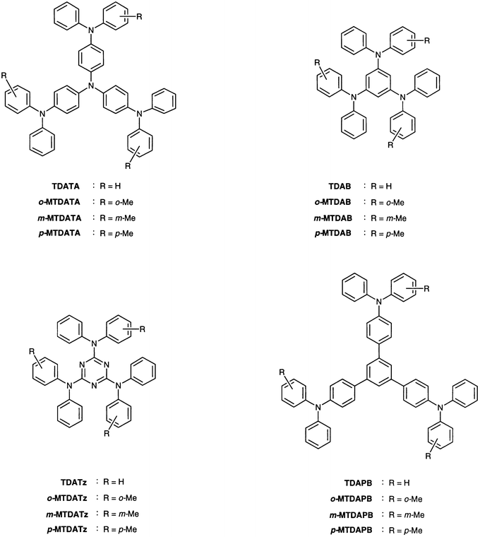
Formation of the glassy state was confirmed by differential scanning calorimetry (DSC), X-ray diffraction (XRD), and polarising microscopy. Fig. 1 shows the DSC curves of m-MTDATA as an example. When a polycrystalline sample of m-MTDATA obtained by recrystallisation from THF–ethanol was heated, an endothermic peak due to melting was observed at 203![[thin space (1/6-em)]](https://www.rsc.org/images/entities/char_2009.gif) °C. When the isotropic liquid was cooled down on standing in air, a transparent glass was spontaneously formed via a supercooled liquid. When the amorphous glass sample was again heated, a glass-transition phenomenon was observed at 75°C. On further heating above the glass-transition temperature (Tg), an exothermic peak due to crystallisation was observed at ca. 160°C to give the same crystal as obtained by recrystallisation from solution, which melted at 203°C.20 The same DSC curves were reproduced repeatedly.
°C. When the isotropic liquid was cooled down on standing in air, a transparent glass was spontaneously formed via a supercooled liquid. When the amorphous glass sample was again heated, a glass-transition phenomenon was observed at 75°C. On further heating above the glass-transition temperature (Tg), an exothermic peak due to crystallisation was observed at ca. 160°C to give the same crystal as obtained by recrystallisation from solution, which melted at 203°C.20 The same DSC curves were reproduced repeatedly.
 | ||
| Fig. 1 DSC curves of m-MTDATA. | ||
 | ||
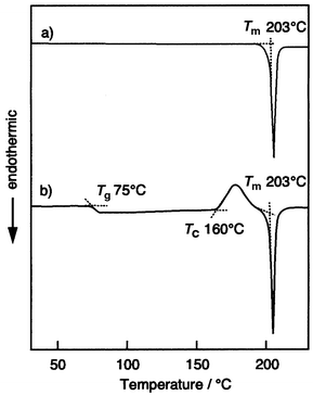
| Fig. 2 Molecular structure of TDATA. | ||
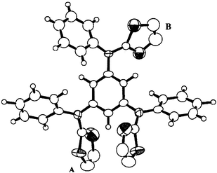 | ||
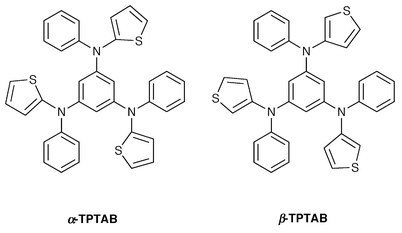
| Fig. 3 Molecular structure of α-TPTAB. The population ratios of the disordered thienyl groups A and B are 0.73∶0.27, and 0.32∶0.18, respectively (see text). | ||
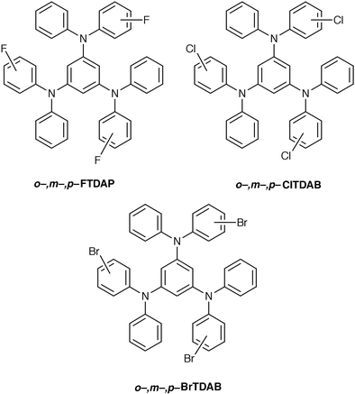
The nonplanar molecular structure is responsible for the glass formation, but not all compounds with nonplanar molecular structures necessarily show glass formation, as exemplified by TDAB, TDATz, and p-MTDATz, which instantly crystallise instead of forming glasses even when the melt samples are rapidly cooled with liquid nitrogen. However, incorporation of substituents exerts a great influence on the ease of glass formation. That is, introduction of alkyl or halogen substituents into TDAB and TDATz or the replacement of three phenyl groups in TDAB by three thienyl groups permitted the formation of glasses by cooling the melt samples either with liquid nitrogen (for p-MTDAB, α- and β-TPTAB) or on standing in air (for o- and m-MTDAB, o- and m-MTDATz).21,28 It should also be noted that whereas TDATA requires rapid cooling with liquid nitrogen for the formation of a glass, its methyl-substituted derivatives, o-, m-, and p-MTDATA, spontaneously form amorphous glasses when the melt samples are cooled on standing in air.20 It is suggested that the incorporation of the methyl or halogen substituents or the replacement of the phenyl group by the thienyl group increases the number of conformers and the mode of packing of molecules, preventing crystallisation and facilitating glass formation. The result of X-ray crystal structure analysis of α- and β-TPTAB that the thienyl group is disordered is also in support of the idea that α- and β-TPTAB can take on different conformations with almost equal conformational energies.28,35 The kind of halogen substituent at the o-, m-, or p-position of XTDABs (X = F, Cl, Br) strikingly affects the ease of glass formation, Tg, and stability of the glassy state.30 The ease of glass formation and the stability of the resulting glass have been found to be enhanced in the order FTDAB ≪ ClTDAB < BrTDAB. The Tg is also affected by the type of halogen atom, increasing in the order FTDAB < ClTDAB < BrTDAB. The easier glass formation and enhanced stability of the resulting glass in the order F ≪ Cl < Br are understood in terms of the bulkiness and weight of the halogen atom. That is, the more bulky and heavier halogen atom will prevent the easy packing of molecules and diffusion of molecules in the process of crystal growth, and hence prevent crystallisation. The incorporation of a heavier halogen atom will tend to hinder translational, rotational, and vibrational motions of the molecule, leading to an increase in Tg.
The stability of the glassy state is enhanced with increasing molecular size. Tri(biphenyl-4-yl)amine (TBA) forms a glass;40,42 however, it tends to crystallise in several days at room temperature. On the other hand, the glassy state of m-MTDATA is very stable at room temperature without any crystallisation for more than 10 years. Whereas the glass of p-MTDAB tends to crystallise in several months on standing in air at room temperature, the amorphous glasses of 1,3,5-tris[4-diphenylaminophenyl(phenyl)amino]benzene (p-DPA-TDAB)26 and 1,3,5-tris{N-[4-bis(4-methylphenyl)aminophenyl]-N-(4-diphenylaminophenyl)amino}benzene (MTBDAB)34 are very stable without any crystallisation even on heating above their Tgs.
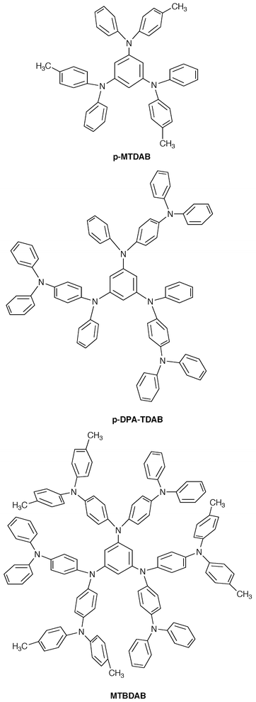
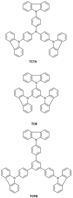
The Tg of molecular glasses is understood as the temperature at which molecular motions of a group of molecules, which are caused by intramolecular bond rotations, start to take place, resulting in a change in the position of the gravity of molecules. In applying amorphous molecular materials for electronic and optoelectronic devices, thermal stability is often required. It is thus necessary to develop amorphous molecular materials with high Tgs. We have shown that Tg can be increased by the incorporation of a structurally rigid moiety, that is, by decreasing the flexibility of nonplanar molecules.24,27,31–33 For example, when the diphenylamino group in the TDAB, TDATA, and TDAPB families is replaced by a rigid carbazolyl group, the Tg increases by approximately 70°C. In addition, Tg increases with increasing molecular size and weight,26,34 and by the introduction of heavy substituents. Introduction of intermolecular interactions such as hydrogen bonding or dipolar interactions also provides an approach for increasing Tg.
Very recently, a number of new amorphous molecular materials, e.g., π-electron starburst molecules containing oxadiazole and quinoxaline moieties,58–60 spiro-linked compounds based on π-electron systems,61,62 dendrite macromolecules,63,64 and others,65 have been developed. Some of them function as materials for organic EL devices.
| Compound | Tg/°C | Tc/°C | Tm/°C |
|---|---|---|---|
| aExhibits polymorphism. bTm of the crystal with the highest melting point. cNo crystallization on heating from the glass. dObtained as an amorphous glass. | |||
| TDATAa | 89 | 134 | 275b |
| o-MTDATAa | 76 | 153 | 200b |
| m-MTDATA | 75 | 160 | 203 |
| p-MTDATAa | 80 | 130 | 265b |
| TCTAa | 150 | 190 | 296b |
| o-MTDAB | 42 | 121 | 161 |
| m-MTDAB | 47 | 85 | 183 |
| p-MTDAB | 55 | 81 | 210 |
| p-FTDAB | 54 | 66 | 228 |
| p-ClTDAB | 64 | 112 | 181 |
| p-BrTDAB | 72 | —c | 165 |
| α-TPTABa | 38 | 70 | 187b |
| β-TPTABa | 46 | 76 | 210b |
| TCBa | 126 | 164 | 330b |
| p-DPA-TDAB | 107 | —c | 240 |
| MTBDAB | 134 | —c | —d |
| o-MTDATz | 55 | 85 | 175 |
| m-MTDATza | 42 | 67 | 175b |
| TDAPB | 121 | 196 | 269 |
| o-MTDAPB | 109 | 154 | 279 |
| m-MTDAPB | 105 | 167 | 231 |
| p-MTDAPB | 110 | —c | 243 |
| TCPBa | 172 | 215 | 356b |
2.2 Characteristic features of amorphous molecular materials—morphological changes, structures, reactions, and properties
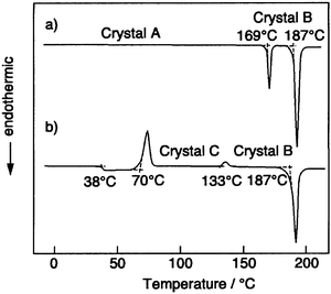
Some characteristic features of amorphous molecular materials with regard to relaxation phenomena, structures, reactions, and solid-state properties are described here.For example, p-MTDAB, α-TPTAB, and β-TPTAB take on three different crystal forms.21,28,35,66Fig. 4 shows DSC curves of α-TPTAB. When a crystalline sample of α-TPTAB obtained by recrystallisation from benzene–hexane or cyclohexane (crystal A) was heated, an endothermic peak due to a solid–solid phase transition was observed at 169°C, where the crystal A was transformed into a different crystal form (crystal B). On further heating, the crystal B melted at 187°C to give an isotropic liquid. When the isotropic liquid was rapidly cooled with liquid nitrogen, a transparent glass was formed. When the amorphous glass was again heated, a glass-transition phenomenon was observed at 38°C, and then an exothermic peak due to crystallisation to form another crystal (crystal C) was observed around 70°C. Thereafter, an exothermic peak due to a solid–solid phase transition from the crystal C to the crystal B was observed around 133°C, followed by the melting of the crystal B at 187°C. It is of interest to note that the mode of phase transformation is different between α-TPTAB and β-TPTAB. While α-TPTAB undergoes solid–solid phase transitions from the crystal C to the crystal B, β-TPTAB undergoes phase transitions involving melting and crystallisation. In the case of p-MTDAB, phase transition involves melting followed by crystallisation.66 The morphological changes of α-TPTAB are summarized in Scheme 1.
 | ||
| Fig. 4 DSC curves of α-TPTAB. | ||
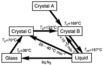 | ||
| Scheme 1 Morphological changes of α-TPTAB. | ||
As described above, it has been demonstrated that the relaxation of the molecular glass is characterised by well-defined glass transition, followed by either solid–solid or melting–crystallisation phase transformations, finally leading to the formation of the crystal with the highest melting point. The phenomena of polymorphism observed for many amorphous molecular materials suggest the existence of different conformers, which is responsible for the ready formation of the glassy state.
°C (m-MTDATA: 80 Å3, m-MTDAPB: 87 Å3, polystyrene: 120 Å3) and that the average size of the free volume hole of molecular glasses increases with increasing molecular size. The temperature dependence of PAL showed that the temperature at which the slope of the plot of the lifetime of o-Ps versus temperature increased steeply corresponds to the glass-transition temperature. The size of free volume may affect reactions in the molecular glass and its properties.It was found that DAAB dispersed in the film of m-MTDATA or TCTA amorphous glass undergoes reversible photoisomerisation. The cis-fractions of DAAB at the photostationary state at 30°C were estimated to be ca. 0.26 and 0.27 for the m-MTDATA and TCTA films containing a 0.01 molar ratio of DAAB. These values are smaller than those (0.85) in solution and in a polystyrene glass.
It is also notable that the apparent rate constant at the initial stage of the backward thermal cis–trans isomerisation of DAAB in these molecular glasses was larger than those in the polystyrene matrix and benzene solution, as shown in Fig. 5. In contrast to the reaction in benzene solution which followed first-order kinetics, the backward thermal cis–trans isomerisation of DAAB in the films of molecular glass and polystyrene did not follow first-order kinetics, being analyzed by the first-order kinetics of two components. The rate constant of the slower component obtained for the m-MTDATA, TCTA, and polystyrene films was equal to that of the benzene solution. The fractions of the faster component were considerably larger for the m-MTDATA and TCTA films than for the polystyrene matrix film; this leads to the faster apparent rate constant at the initial stage for the m-MTDATA and TCTA amorphous films than for the polystyrene matrix film. Table 2 lists the kinetic parameters obtained for the reactions in the m-MTDATA and TCTA glasses, the polystyrene matrix, and the benzene solution. The slower component is attributed to the reaction of the photogenerated, structurally relaxed cis-isomer and the faster component is thought to be attributable to the reaction of the photogenerated cis-isomer with a strained conformation due to the presence of the surrounding matrix which restricts the molecular motion of DAAB.
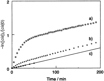 | ||
| Fig. 5 First-order plots for the thermal cis–trans isomerisation of DAAB in (a) m-MTDATA film, (b) polystyrene film, (c) benzene solution (3.3 × 10⁻⁴ mol dm−3) at 30°C after the reaction system has reached the photostationary state upon irradiation with 400 nm light. | ||
°C in the molecular glasses, polystyrene, and benzene solutiona
| Reaction medium | k1/min−1 | f1 | k2/min−1 | f2 |
|---|---|---|---|---|
| aAnalyzed by the first-order kinetics of two components: [cis]t/[cis]0 = f1 exp(−k1t) + f2 exp(−k2t). b0.01 molar ratio of DAAB. cSingle component. | ||||
| m-MTDATA filmb | 0.083 | 0.54 | 0.003 | 0.46 |
| TCTA filmb | 0.032 | 0.35 | 0.003 | 0.65 |
| Polystyrene film | 0.062 | 0.12 | 0.003 | 0.88 |
| Benzene solutionc | — | — | 0.003 | 1.00 |
These results suggest that the size of local free volume in the m-MTDATA and TCTA host matrices is smaller than that in the polystyrene glass. Therefore, a large number of trans-DAAB molecules remain unchanged in these molecular glass matrices at the photostationary state and the proportion of strained cis-isomer relative to the relaxed one is large in these molecular glasses. The result of the reaction in molecular glasses is in agreement with the result of the free volume size estimated by the PAL technique.
It has recently been shown that charge transport in molecularly-doped polymer systems is greatly dependent upon the binder polymer. In fact, the hole drift mobility of molecularly-doped polymer systems has been reported to vary by two orders of magnitude depending upon the binder polymer.78–80 Charge–dipole interactions between a charge on the transport molecule and the binder polymer are thought to cause the fluctuation of both the hopping site energy and the overlap integral. In order to clarify intrinsic charge-transport properties of low molecular-weight organic materials in the disordered system, charge transport in the amorphous glassy state of low molecular-weight organic materials in the absence of a binder polymer should be investigated.
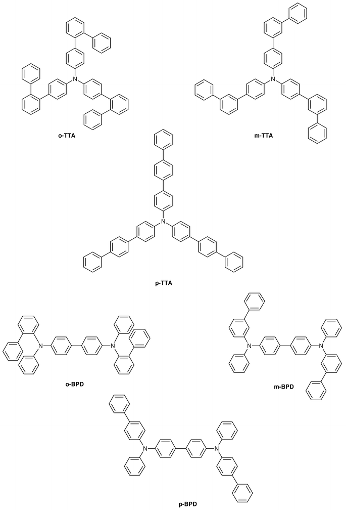
Creation of amorphous molecular materials has made it possible to investigate charge transport in the glassy state. We have measured charge-carrier drift mobilities of a variety of molecular glasses.23,40–44,57,81–91Table 3 lists the hole drift mobilities of some molecular glasses. It is shown that the hole drift mobilities of molecular glasses are in the order from 10−6 to 10−2 cm2 V−1 s−1 at an electric field of 1.0 × 10⁵ V cm−1 at room temperature. o-MTDAB, p-BPD, and tris[4-(2-thienyl)phenyl]amine exhibit high hole drift mobilities exceeding 1.0 × 10⁻³ cm2 V−1 s−1 and tris[4-(5-phenyl-2-thienyl)phenyl]amine the highest mobility of 1.0 × 10⁻² cm2 V−1 s−1 at an electric field of 1 × 10⁵ V cm−1 at 293 K.81,90 Although the values of hole drift mobilities vary greatly depending upon molecular structure, higher drift mobilities of amorphous molecular materials relative to those of polymers and molecularly-doped polymer systems may be attributed to the absence of dilution effects of hopping sites and to the absence of charge–dipole interactions between charge carriers and the binder polymer.
| Material | μh/cm2 V−1 s−1 |
|---|---|
| Measured at an electric field of a1.0 × 105 V cm−1 and b2.0 × 105 V cm−1 at 293 K. | |
| m-MTDATA | 3.0 × 10⁻⁵a |
| o-MTDAB | 3.0 × 10⁻³b |
| p-DPA-TDAB | 1.4 × 10⁻⁴b |
| MTBDAB | 2.5 × 10⁻⁵b |
| m-MTDAPB | 1.6 × 10⁻⁵b |
| o-TTA | 7.9 × 10⁻⁴a |
| m-TTA | 2.3 × 10⁻⁵a |
| p-TTA | 8.8 × 10⁻⁴a |
| o-BPD | 6.5 × 10⁻⁴a |
| m-BPD | 5.3 × 10⁻⁵a |
| p-BPD | 1.0 × 10⁻³a |
| BMA-3T | 2.8 × 10⁻⁵a |
| BMA-4T | 1.0 × 10⁻⁵a |
We have studied the relationship between molecular structure and charge-transport properties in order to gain information on the guidelines for the molecular design of amorphous molecular materials with high drift mobility.81 A few examples are given here. The charge-carrier drift mobility greatly varies depending upon the position of the phenyl group in the biphenyl moiety. Hole drift mobilities of the o- and p-isomers of TTA and BPD have been found to be more than one order of magnitude larger than those of the m-isomers of TTA and BPD (Table 3). The analysis of the electric-field and temperature dependencies of the drift mobilities of these materials in terms of the disorder formalism showed that the difference in the energetic disorder σ is responsible for the difference in the hole drift mobility among o-, m-, and p-isomers: the σ value significantly increases in the order o-TTA (0.059 eV) < p-TTA (0.071 eV) < m-TTA (0.093 eV) and o-BPD (0.071 eV) < p-BPD (0.075 eV) < m-BPD (0.105 eV).57
It is thought that the degree of the variation of the molecular geometry caused by the rotation along the C–C and C–N bonds is responsible for the difference in the σ value among the o-, m-, and p-isomers; the smaller variation of the molecular geometry results in the smaller energetic disorder σ. The variation of the molecular geometry may be much smaller for o- and p-isomers than that for the m-isomer due to the restricted internal rotation in the o-terphenyl moiety for the o-isomers and to the smaller number of conformers resulting from the bond rotation for the symmetrical p-isomer. Thus, decreasing the variation of molecular geometry by restricting internal rotation or by increasing the symmetry of the molecule is suggested to be a guiding principle for the molecular design for high mobility.
The effect of molecular size on the charge-carrier drift mobility was studied using a novel family of molecular glasses having a similar molecular skeleton but a varying molecular size, o-MTDAB, p-DPA-TDAB, and MTBDAB. It was found that the hole drift mobilities of these molecular glasses vary by two orders of magnitude depending on the molecular size: the hole drift mobility increased with decreasing molecular size in the order MTBDAB < p-DPA-TDAB < o-MTDAB. o-MTDAB exhibited a high mobility of 3 × 10⁻³ cm2 V−1 s−1 at an electric field of 2.0 × 10⁵ V cm−1 at 293 K.91
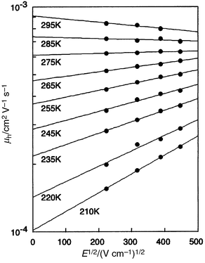
The drift mobility (μ) of charge carriers generally increases with increasing electric field (E), following the relation ln μ ∝ exp(SE1/2), where S is a coefficient. We have found for the first time the negative electric-field dependence of charge-carrier drift mobility with regard to molecular glasses.43 As Fig. 6 shows, the molecular glass of o-TTA exhibited the negative electric-field dependence of hole drift mobility. The hole drift mobility of the o-TTA glass increased with increasing electric field in a temperature range below 285 K, following the electric-field dependence of exp(SE1/2); however, the hole drift mobility started to decrease with increasing electric field above 285 K. The negative electric-field dependence of charge-carrier drift mobility is understood as arising from the contribution of the diffusion process of charge carriers against the direction of electric field due to the presence of positional disorder Σ caused by the disorder of the intermolecular π-electron overlap. That is, faster detour routes against the electric field exist due to the presence of the positional disorder Σ. The rate of the diffusion of charge carriers through the detour routes increases with rising temperature because of the growing mean energy of charge carriers. However, the diffusion rate gradually decreases with increasing electric field; this results in the negative electric-field dependence of charge-carrier drift mobility. The analysis of the electric-field and temperature dependencies of drift mobilities in the temperature range below 285 K in terms of the disorder formalism gave the following hole-transport parameters for the molecular glass of o-TTA: μ0 = 9.7 × 10⁻³ cm2V–1 s−1, σ = 0.059 eV, Σ = 2.4, and C = 4.4 × 10⁻⁴ (cm V−1)1/2. The small σ value as well as the presence of the positional disorder Σ is responsible for the negative electric-field dependence of the drift mobility of the o-TTA glass. The negative electric-field dependence of drift mobility was also observed for m-MTDATA.88,89
 | ||
| Fig. 6 Electric-field dependence of the hole drift mobilities of the o-TTA glass at various temperatures. | ||
Studies of charge transport and in particular, the observation of the negative electric-field dependence of charge-carrier drift mobility have verified the presence of the disorder of intermolecular distance and orientation in amorphous molecular materials.
Very recently, charge transport in vacuum deposited amorphous films has also been studied. The values of hole and electron drift mobilities are mostly in the range from 10−5 to 10–3 cm2 V–1 s–1.92–97
2.3 Functions and applications of amorphous molecular materials
We have created several novel classes of functional amorphous molecular materials, e.g., electrically conducting amorphous molecular materials, photochromic amorphous molecular materials, molecular resists, amorphous molecular materials for photovoltaic and organic EL devices.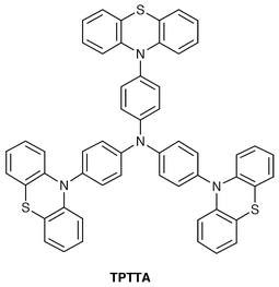
A transparent amorphous film of TPTTA formed by cooling the melt sample or by solvent cast was exposed to iodine vapor for three days in a glass tube to give a black, lustrous film. It was proved to be an amorphous glass, as characterised by DSC and XRD. The chemically-doped amorphous film was identified as a TPTTA radical-cation salt with I3− and I5− as dopants, as characterised by IR, Raman, and electronic absorption spectroscopy. The iodine-doped amorphous glass, (TPTTA)I2.6, exhibited a room-temperature conductivity of 1 × 10⁻⁵ S cm−1 with an activation energy of 0.36 eV.
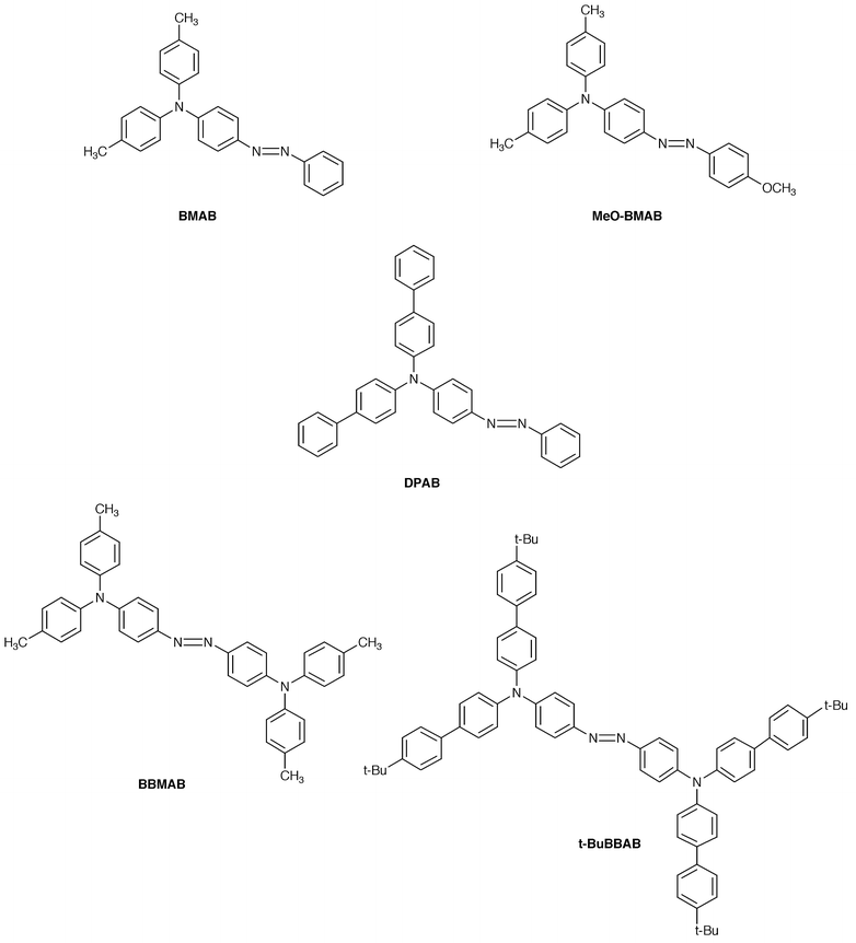
Based on this concept, we have created a novel family of photochromic amorphous molecular materials containing an azobenzene chromophore.48–51 It includes 4-[bis(4-methylphenyl)amino]azobenzene (BMAB), 4-[bis(4-methylphenyl)-amino]-4′-methoxyazobenzene (MeO-BMAB), 4-[di(biphenyl-4-yl)amino]azobenzene (DBAB), 4,4′-bis[bis(4-methylphenyl)amino]azobenzene (BBMAB), and 4,4′-bis[bis(4′-tert-butylbiphenyl-4-yl)amino]azobenzene (t-BuBBAB). These compounds were found to readily form amorphous glasses with Tgs of 27, 33, 68, 79, and 177°C, respectively, and to exhibit photochromism in their amorphous films. Photoisomerisations from trans- to cis- and cis- to trans-isomers took place repeatedly under alternating irradiation with 450 and 550 nm light each for one minute (Fig. 7). The fractions of cis-isomer at the photostationary state in the amorphous film were 0.54, 0.29, 0.53, 0.17, and 0.15 for BMAB, MeO-BMAB, DBAB, BBMAB, t-BuBBAB, respectively. The photogenerated cis-form undergoes thermal isomerisation to the trans-form. Stabilisation of the photogenerated cis-form at ambient temperature was attained by the incorporation of a bulky group. More than 80% of the photogenerated cis-form of t-BuBBAB remained unchanged after five days at room temperature; however, the cis-form was completely transformed into the trans-form by heating the sample to 140°C. Thus, the backward cis–trans thermal isomerisation can be controlled by temperature.50
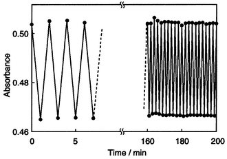 | ||
| Fig. 7 Change of absorbance at 430 nm for amorphous BMAB film under alternating irradiation with 450 nm and 550 nm light at 20°C. | ||
Based on this idea, we have designed and synthesized several novel classes of molecular resist materials that form uniform amorphous films, 1,3,5-tris[4-(4-tolylsulfonyloxy)phenyl]benzene (TsOTPB), 1,3,5-tris[2-(tert-butoxycarbonyloxy)phenyl]benzene (o-BCOTPB), 1,3,5-tris[4-(tert-butoxycarbonyloxy)-phenyl]benzene (p-BCOTPB), 4,4′,4″-tris(allylsuccinimido)triphenylamine (ASITPA), and 1,3,5-tris[4-(4-vinylphenylcarbonyloxy)phenyl]benzene (VCTPB). TsOTPB, o- and p-BCOTPB have been found to function as positive resists and ASITPA and VCTPB as negative resists with high resolution capability on exposure to an electron beam.53–56 Related to this work, an oligomer of a calixarene derivative has been reported to function as a negative electron-beam resist with high resolution.100
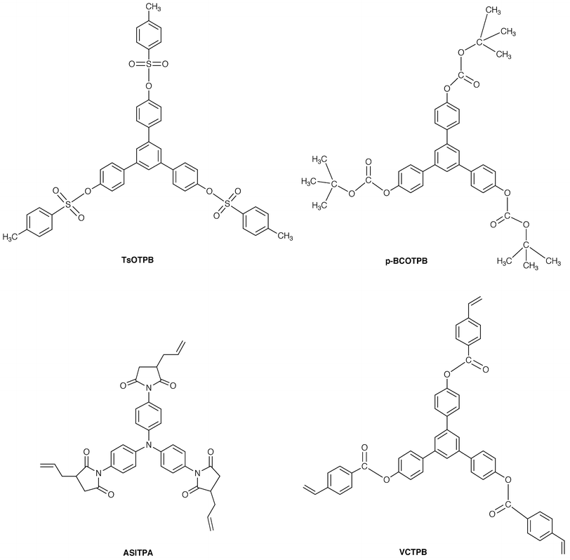
Line patterns of 150, 70, and 40 nm could be fabricated for the TsOTPB positive resist, ASITPA negative resist, and p-BCOTPB positive resist, respectively. p-BCOTPB showed a high sensitivity of 4.4 µC cm−2. Fig. 8 shows the SEM images of negative-tone line and space patterns for the ASITPA film and positive-tone line and space patterns for the p-BCOTPB film. Molecular resist materials are expected to be promising candidates for the future nanometre lithography.
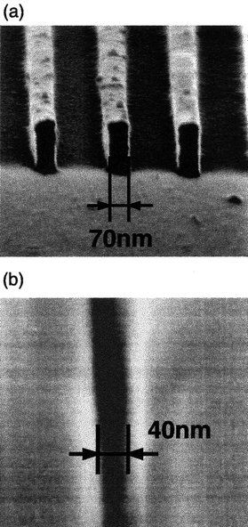 | ||
| Fig. 8 (a) SEM image of negative-tone line and space patterns for the ASITPA resist film on exposure to 50 keV electron beam at 12 mC cm−2. (b) SEM image of positive-tone line and space patterns for the p-BCOTPB resist film on exposure to 50 keV electron beam at 200 µC cm−2. | ||
°C, respectively, and that the absorption bands of these compounds extend to the wavelength range of visible light. p–n Heterojunction devices using MNTDATA or MB-TPA as a p-type material and anthra[2″,1″,9″∶4,5,6; 6″,5″,10″∶4′,5′,6′]diisoquino[2,1-a∶2′,1′-a′]dibenzimidazole-10,21-dione (PV) as an n-type material were found to respond to visible light, exhibiting conversion efficiencies of 0.4 and 0.1%, respectively, when irradiated with monochromatic light of 440 nm which MNTDATA and MB-TPA mainly absorb.101,102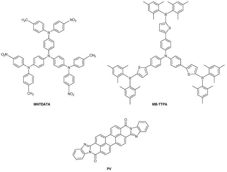
(a) Hole-transporting amorphous molecular materials. With regard to low molecular-weight hole-transporting materials for organic EL devices, N,N′-bis(3-methylphenyl)-N,N′-diphenyl-[1,1′-biphenyl]-4,4′-diamine (TPD) has been widely used; however, TPD lacks thermal and morphological stability. It is desirable that the materials should have high Tgs for attaining thermal stability of organic EL devices. We have created several novel families of hole-transporting amorphous molecular materials with higher Tgs, which include the TDATA family, e.g., m-MTDATA,20 the naphthyl- or biphenyl-substituted derivatives of TDATA, 1-TNATA,33 2-TNATA,33o-PTDATA,36m-PTDATA,36p-PMTDATA,36 and TCTA,27 and the TDAB and TDAPB families, e.g., p-DPA-TDAB,26 MTBDAB,34 and the o-, m-, and p-methyl substituted derivatives of TDAPB (o-, m-, and p-MTDAPB).23 Very recently, new TPD derivatives with Tgs higher than that of TPD have been developed. They are the naphthyl-, phenanthryl-, and biphenyl-substituted derivatives, N,N′-di-(1-naphthyl)-N,N′-diphenyl-[1,1′-biphenyl]-4,4′-diamine (α-NPD),105N,N′-di(9-phenanthryl)-N,N′-diphenyl-[1,1′-biphenyl]-4,4′-diamine,106o-BPD,57m-BPD,57 and p-BPD.57 In 1994, we reported for the first time the thermal stability of an organic EL device using TCTA as the hole-transporting layer and tris(quinolin-8-olato)aluminum (Alq3) as the emitting layer, showing that the device operates at 150
°C, whereas the double-layer device using TPD and Alq3 ceased emission when the temperature rose to 65°C.27 Thermally stable organic EL devices have been developed using hole-transporting amorphous molecular materials with high Tgs in combination with Alq3 as an emitting material.32,36,107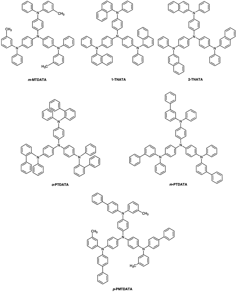
We reported in 1994 that a multilayer organic EL device consisting of an emitting layer of Alq3 and double hole-transporting layers of m-MTDATA and TPD, ITO/m-MTDATA/TPD/Alq3/MgAg, exhibits higher luminous efficiency and significantly enhanced operational stability than double-layer devices consisting only of an emitting layer of Alq3 and a single hole-transport layer of TPD,108 paving the way for durable organic EL devices. While the double-layer device consisting of a single hole-transport layer of TPD and an emitting layer of Alq3 generates a leak current in a short time during operation, multilayer devices using the m-MTDATA or 1-TNATA layer in contact with the ITO electrode operate safely without generating a leak current. The ITO/m-MTDATA(600 Å)/TPD(100 Å)/Alq3(500 Å)/MgAg device exhibited a maximum luminescence of 24000 cd m−2 at an applied voltage of 15 V and a luminous efficiency of 2.4 lm W−1. The multilayer structure as shown in Fig. 9 has since been widely employed for fabricating organic EL devices with high operational stability, where HTL1 acts as a hole-injection layer. The materials of the TDATA family, e.g., m-MTDATA, 1-TNATA, 2-TNATA, o-, m-PTDATA and p-PMTDATA, which are characterised by very low ionisation potentials and the good quality of their amorphous films, function as an excellent hole injection layer in contact with the ITO electrode. The materials with higher ionisation potentials such as TPD, α-NPD, o-, m-, and p-BPD, TCTA, p-DPA-TDAB, and o-, m-, and p-MTDAPB function as materials for HTL2. The half-decay time of the initial luminescence of 300 cd m−2 was 2000 h at room temperature for the multilayer device, ITO/m-MTDATA/α-NPD/Alq3/MgAg. The device consisting of double hole-transport layers of p-PMTDATA and p-BPD and an Alq3 emitting layer exhibited high performance and significant thermal stability: the device operated at 150°C, retaining a luminance of 80% of the initial value measured at 20°C (Fig. 10).36 It has been shown that doping of an intense fluorescent molecule in the emitting material Alq3 improves not only the luminous efficiency but also the thermal and operational stability of organic EL devices using 1-TNATA as HTL1.109
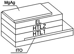 | ||
| Fig. 9 Multilayer organic EL device consisting of the double hole-transport layers and the emitting layer. EL: emitting layer, HTL: hole transport layer. | ||
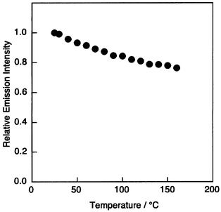 | ||
| Fig. 10 Temperature dependence of luminance of the multilayer device, ITO/p-PMTDATA/p-BPD/Alq3/MgAg. Measured in a cryostat at 10−3 Torr. | ||
(b) Electron-transporting amorphous molecular materials. Electron-transporting materials can be used in combination with emitting materials either with weaker electron-accepting properties or with hole-transporting properties. As compared with hole-transporting materials, there have been few examples of electron-transporting materials, which include Alq3, oxadiazole derivatives,33,58,110 3-(biphenyl-4-yl)-4-phenyl-5-(4-tert-butylphenyl)-1,2,4-triazole,111 and 1,1′-dimethyl-2,5-di(2-pyridyl)silole.112
We have created novel families of thermally stable, electron-transporting amorphous molecular materials, 1,3,5-tris(4-tert-butylphenyl-1,3,4-oxadiazolyl)benzene (TPOB),33,58 1,3,5-tris[5-(dimesitylboryl)-2-thienyl]benzene (TMB-TB),113 5,5′-bis(dimesitylboryl)-2,2′-bithiophene (BMB-2T),46 and 5,5″-bis(dimesitylboryl)-2,2′∶5′,2″-terthiophene (BMB-3T).46 These compounds readily form stable amorphous glasses with Tgs of 137, 160, 107, and 115°C, respectively.
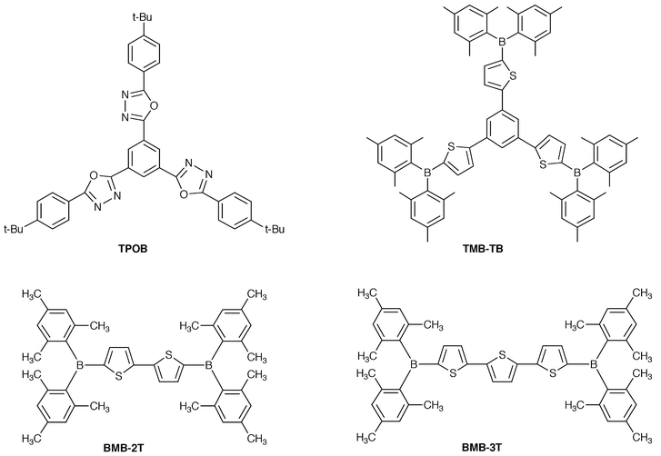
Both BMB-2T and BMB-3T function as excellent electron-transporting materials in combination with an emitting material Alq3 to enhance the performance of the organic EL devices.46 Multilayer organic EL devices using BMB-2T or BMB-3T as an electron-transporting material, Alq3 as an emitting material, and m-MTDATA and α-NPD as hole-transporting materials, ITO/m-MTDATA(300 Å)/α-NPD(200 Å)/Alq3(300 Å)/BMB-nT (n = 2 or 3)(200 Å)/MgAg, emitted bright green light originating from the electronically excited singlet state of Alq3, exhibiting approximately 10 to 20% higher luminous and quantum efficiencies and 1.6 to 1.8 times higher maximum luminance than the organic EL device without the BMB-nT layer, ITO/m-MTDATA(300 Å)/α-NPD(200 Å)/Alq3(500 Å)/MgAg. In multilayer organic EL devices using BMB-nT as an electron-transport layer, electron injection takes place more readily by a stepwise process through the BMB-nT layer.
(c) Emitting amorphous molecular materials. Organic EL devices permit multi-colour or full-colour emission by the selection of emitting materials. With regard to low molecular-weight organic emitting materials, Alq3 has been used most extensively as a green-emitting material with electron-transporting properties. In order to achieve full-colour emission, red, green, and blue emissions are needed.
Blue-emitting low molecular-weight organic materials which have been reported include 1,3-bis[4-(N,N-dimethylamino)phenyl-1,3,4-oxadiazolyl]benzene,110 4,4′-bis(2,2-diphenylethenyl)-biphenyl,114 3-(biphenyl-4-yl)-5-(4-dimethylamino)-4-(4-ethylphenyl)-1,2,4-triazole,115 and 2,2′,7,7′-tetra(biphenyl-4-yl)-9,9′-spirobifluorene.61 Organic EL devices using these blue-emitting materials have been reported to exhibit brightness of approximately 1000 cd m−2 except for 4,4′-bis(2,2-diphenyl-ethenyl)biphenyl, which exhibits much higher luminance.
We have created novel blue-emitting amorphous molecular materials, tri(p-terphenyl-4-yl)amine (p-TTA),42 tri(o-terphenyl­4-yl)amine (o-TTA)43 and BMB-2T.46o- and p-TTA have hole-transporting properties and BMB-2T has electron-transporting properties. They display intense blue fluorescence with quantum efficiencies of 0.48, 0.68 and 0.86 in THF solution.
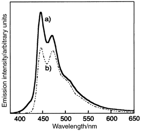
p-TTA functions not only as a blue-emitting material but also as a good host material for fluorescent dopants, e.g., perylene. A bilayer organic EL device using p-TTA as a blue-emitting material and p-DPA-TDAB as a hole-transporting material emitted blue light resulting from p-TTA116 and a bilayer device using perylene-doped TTA, ITO/p-DPA-TDAB (600 Å)/perylene (5 mol%) doped p-TTA (600 Å)/MgAg, emitted bright blue light resulting from perylene instead of p-TTA.117 Whereas the EL spectrum of the undoped device was in accordance with the PL spectrum of p-TTA, that of the perylene-doped device was in good agreement with the fluorescence spectrum of perylene in a dilute solution. Fig. 11 shows the EL spectra of the perylene-doped and undoped organic EL devices. The device exhibited a maximum luminance of 2400 cd m−2 at a driving voltage of 17 V and a luminous efficiency of 0.5 lm W−1 at a luminance of 100 cd m−2. The emission started at an applied voltage of approximately 5 V. The external quantum efficiency was estimated to be 0.8%.
 | ||
| Fig. 11 EL spectra of (a) ITO/p-DPA-TDAB(600 14;Å)/p-TTA(600 Å)/MgAg and (b) ITO/p-DPA-TDAB(600 Å)/perylene(5 mol%) doped p-TTA(600 Å)/MgAg devices, and (c) PL spectrum of perylene. | ||
BMB-2T functions not only as an excellent electron-transporting material but also as a novel blue-emitting material for organic EL devices. Blue-emitting BMB-2T was found to form exciplexes with hole-transporting materials such as TPD; however, the exciplex formation was prevented by the insertion of a thin layer of a new amorphous molecular material, 1,3,5-tri(biphenyl-4-yl)benzene (TBB) (Tg = 88°C), in between the hole-transport layer of TPD and the emitting layer of BMB-2T.118 The multilayer device consisting of m-MTDATA, TPD, TBB, and BMB-2T exhibited blue emission from BMB-2T with a maximum luminescence of 1100 cd m–2.
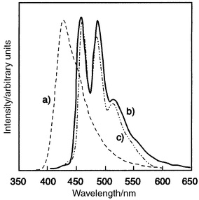
The combination of two kinds of blue-emitting materials with electron-transporting and hole-transporting properties, BMB-2T and o- or p-TTA, resulted in the blue-emission mainly from BMB-2T.119 A triple-layer organic EL device using m-MTDATA as a hole-injection layer, o-TTA or p-TTA as a hole-transport layer, and BMB-2T as an emitting layer, ITO/m-MTDATA(300 Å)/TTA(200 Å)/BMB-2T(300 Å)/MgAg(1000 Å), emitted blue light resulting mainly from BMB-2T and partly from o- or p-TTA. Fig. 12 shows the EL spectrum of the device together with the PL spectrum of the amorphous thin film of BMB-2T. The EL spectrum with λmax at 446 and 472 nm is in accordance with the PL spectrum of the film of BMB-2T. A very weak emission with λmax at approximately 410 nm resulting from o-TTA was also observed. Neither exciplex emission in the longer wavelength was observed nor was the EL spectrum affected by the magnitude of the applied voltage. As suggested from Tables 4a and b, the energy barrier for electron injection from the BMB-2T layer into the o-TTA layer is thought to be higher than that for the hole injection from the o-TTA layer into the BMB-2T layer, and hence the recombination of holes and electrons takes place mainly in the layer of BMB-2T to generate the electronically excited singlet state of BMB-2T.
 | ||
| Fig. 12 (a) EL spectrum of ITO/m-MTDATA(300 Å)/o-TTA(200 Å)/BMB-2T(300 Å)/MgAg(1000 Å) device and (b) PL spectrum of BMB-2T. | ||
| Compound | E1/2oxa/Vd | λmax(abs)b/nm | Band gapc/eV | λmax(em)b/nm | Tg/°C |
|---|---|---|---|---|---|
| aMeasured in dichloromethane solution containing tetrabutylammonium perchlorate. bMeasured in tetrahydrofuran solution. cEstimated from the electronic absorption edge. dvs. Ag/Ag+ (0.01 mol dm−3). eEp/2. | |||||
| m-MTDATA | 0.06 | 342 | 3.20 | 427 | 75 |
| t-Bu-TBATA | 0.09 | 353 | 3.12 | 465 | 203 |
| o-PTDATA | 0.06 | 346 | 3.15 | 479 | 93 |
| m-PTDATA | 0.10 | 339 | 3.19 | 490 | 91 |
| p-PMTDATA | 0.08 | 341 | 3.14 | 480 | 110 |
| 1-TNATA | 0.08 | 338 | 2.97 | 521 | 113 |
| 2-TNATA | 0.11 | 325 | 3.02 | 486 | 110 |
| TPD | 0.48 | 352 | 3.19 | 399 | 62 |
| o-TTA | 0.61 | 338 | 3.32 | 411 | 81 |
| m-TTA | 0.64 | 347 | 3.25 | 409 | 80 |
| p-TTA | 0.58 | 361 | 3.11 | 435 | 132 |
| o-BPD | 0.48 | 353 | 3.19 | 396 | 75 |
| m-BPD | 0.51 | 351 | 3.20 | 399 | 81 |
| p-BPD | 0.50 | 358 | 3.16 | 406 | 102 |
| TCTA | 0.69e | 326 | 3.44 | 385 | 150 |
| m-MTDAPD | 0.66e | 342 | 3.32 | 408 | 105 |
| p-MTDAPB | 0.64 | 343 | 3.31 | 412 | 110 |
| p-DPA-TDAB | 0.23 | 310 | 3.32 | 410 | 107 |
| BMA-1T | 0.39 | 397 | 2.78 | 456 | 86 |
| BMA-2T | 0.39 | 423 | 2.58 | 491 | 90 |
| BMA-3T | 0.38 | 440 | 2.46 | 516 | 93 |
| BMA-4T | 0.35 | 453 | 2.38 | 532 | 98 |
| Compound | E1/2reda/Vd | λmax(abs)b/nm | Band gapc/eV | λmax(em)b/nm | Tg/°C |
|---|---|---|---|---|---|
| aMeasured in dichloromethane solution containing tetrabutylammonium perchlorate. bMeasured in tetrahydrofuran solution. cEstimated from the electronic absorption edge. dvs. Ag/Ag+ (0.01 mol dm−3). eEp/2. fValues of vapor-deposited film. | |||||
| BMB-2T | −1.76 | 402 | 2.81 | 440 | 107 |
| BMB-3T | −1.76 | 437 | 2.55 | 488 | 115 |
| TPOB | −2.10e | 298 | 3.68 | 364 | 137 |
| TMB-TB | −2.04 | 370 | 3.16 | 402 | 160 |
| Alq3 | −2.01 | 395f | 2.7f | 520f | — |
The multilayer organic EL device, ITO/m-MTDATA-(300 Å)/o- or p-TTA(200 Å)/BMB-2T(300 Å)/MgAg(1000 Å), exhibited high performances with maximum luminances of 2400 and 1700 cd m–2 at a driving voltage of 17 V and luminous and external quantum efficiencies of 0.11 and 0.08 lm W−1 and 0.33 and 0.24% for p- and o-TTA, respectively, at a luminance of 300 cd m−2.119 These values are much higher than those reported for blue-emitting organic EL devices using other materials such as OXD8,110p-EtTAZ,115 and spiro-6Φ61 (maximum luminance: ca. 1000 cd m–2).
Oligothiophenes have been reported to function as emitting materials in organic EL devices;120,121 however, their performances are poor. This is probably because oligothiophenes with well-defined structures are crystalline in nature and hence they form polycrystalline films by vacuum deposition or spin coating. The fluorescence quantum efficiencies of polycrystalline films of oligothiophenes are significantly reduced as compared with those of the corresponding solutions. It was expected that the fluorescence quantum efficiency may not be significantly reduced in the amorphous film state.
We have created a novel family of amorphous molecular materials containing an oligothiophene moiety, 2,5-bis-{4-[bis(4-methylphenyl)amino]phenyl}thiophene (BMA-1T), 5,5′-bis{4-[bis(4-methylphenyl)amino]phenyl}-2,2′-bithiophene (BMA-2T), 5,5″-bis{4-[bis(4-methylphenyl)amino]phenyl}-2,2′∶5′,2″-terthiophene (BMA-3T), and 5,5′″-bis{4-[bis(4-methylphenyl)amino]phenyl}-2,2′∶5′,2″∶5″,2′″-quaterthiophene (BMA-4T). They readily form stable amorphous glasses with Tgs of 86, 90, 93, and 98°C, respectively,44,45,47 functioning as colour-tunable emitting materials depending on the length of oligothiophene moieties. It is of interest to note that the HOMO levels of these compounds are more or less the same but the HOMO–LUMO gap progressively decreases with increasing conjugation length of the oligothiophene moiety.
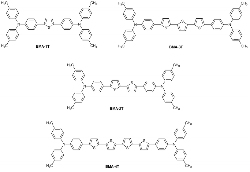
Both single-layer devices using BMA-nT (n = 1–4) alone sandwiched between the ITO and MgAg electrodes and double-layer devices consisting of the emitting layer of BMA-nT (n = 1–4) with hole-transporting properties and the electron-transport layer of Alq3 (for n = 2–4) or TPOB (for n = 1) were fabricated.45,47,122 The EL spectra of both the single-layer and double-layer organic EL devices were in accordance with the PL spectrum of the corresponding BMA-nT (n = 1–4). The EL colour was light blue, yellowish green, yellow, and orange for BMA-1T, BMA-2T, BMA-3T, and BMA-4T, respectively. The double-layer device using BMA-3T and Alq3 exhibited a maximum luminance of 13300 cd m−2 at a driving voltage of 18 V and a luminous efficiency of 1.1 lm W−1 at a luminance of 300 cd m−2. The double-layer organic EL devices showed more than one order of magnitude higher luminous and quantum efficiencies than the corresponding single-layer organic EL devices. It is suggested that in the double-layer device, the electron injection from the MgAg electrode into the BMA-nT (n = 1–4) layer becomes more efficient in the presence of the electron-transport layer of Alq3 or TPOB due to decreased energy barriers.
There is a possibility that exciplex formation takes place at the interface between the electron-transport layer and the hole-transport layer in layered organic EL devices, affecting the emission colour. We have studied exciplex formation at the organic solid/solid interface between electron-transporting and hole-transporting amorphous molecular materials and its application for colour tuning in organic EL devices.123–126 The exciplex formation was evidenced by the measurements of the photoluminescence spectrum and its lifetime for the mixture of an equimolar amount of the electron-transporting and hole-transporting material.
Since the exciplex formation takes place only at the interface between the hole-transport and electron-transport layers, exciplex emission is strengthened for the triple-layer organic EL device with a thin layer of an equimolar mixture of hole- and electron-transporting materials in between the hole-transport and electron-transport layers. The wavelength of exciplex emission varies depending on the electron-donating property of the electron donor and the electron-withdrawing property of the electron acceptor. It is expected that tuning of the emission colour in organic EL devices can be attained by varying the ionisation potential of the hole-transporting material for a fixed electron-transporting material.
Organic EL devices using TPOB or BMB-3T as an electron-transporting material in combination with various hole-transporting amorphous molecular materials with varying ionisation potentials emitted light resulting from the exciplex formed at the solid interface between TPOB or BMB-3T and the hole-transporting material. Tuning of the emission colour from greenish blue to orange was attained by varying the ionisation potential of the hole-transporting material for the fixed electron-transporting material TPOB.123,124 Likewise, the emission colour of the organic EL devices using BMB-3T as the electron-transport layer changed from greenish yellow to orange and red for the hole transport layer of TPD, p-DPA-TDAB, and m-MTDATA, respectively.104
Exciplex formation also takes place at the organic solid interface between Alq3 and hole-transporting amorphous molecular materials with very low ionisation potentials, e.g., m-MTDATA and TNATA (approximately 5.1 eV) to give yellow emission. Because the exciplex emission takes place only at the interface, the emission colour can be turned from yellow to green by varying the magnitude of applied voltage.125,126
3 Titanyl phthalocyanine
Phthalocyanines have found a number of potential applications such as catalysts, charge-carrier generation materials for layered photoreceptors in electrophotography, photosensitisers, gas sensors, liquid crystals, photodynamic cancer therapy, nonlinear optics, photoactive materials for photovoltaic devices, and materials for organic EL devices.1273.1 Characterisation of ultrathin film of TiOPc
The molecular orientation and aggregation as well as the electronic structure of ultrathin films of TiOPc formed by vacuum deposition on graphite and MoS2 substrates have been studied using Penning ionisation electron spectroscopy (PIES) and ultraviolet photoelectron spectroscopy (UPS).128,129 It has been found that in the monolayer partly deposited on graphite (grafoil) at room temperature, all TiOPc molecules are oriented flat to the substrate with the oxygen atom protruding outside the film surface. However, molecules with the oxygen atom directed inside increase in number with increasing coverage with the monolayer. On the other hand, in the monolayer film deposited on MoS2 at room temperature, the TiOPc molecules aggregate. Upon annealing at 370 K, a uniform monolayer with the oxygen atom protruding outside is formed.3.2 Photovoltaic devices using TiOPc
A two-layer device using thin films of copper phthalocyanine (CuPc) and a perylene pigment (PV) sandwiched between the ITO and silver as electrodes, ITO/CuPc/PV/Ag, has been reported to exhibit a high conversion efficiency of 0.95% under simulated AM2 illumination at 75 mW cm−2.130We have studied titanyl phthalocyanine (TiOPc) for use in organic solar cells.131–134 The use of TiOPc as a photoactive material for photoelectric conversion is of interest from the following viewpoints. It was expected that the judicious choice of n-type organic semiconductors in combination with TiOPc permits the fabrication of p–n heterojunction devices that exhibit high conversion efficiencies in view of the fact that TiOPc is used as charge-carrier generation layer in photoreceptors and that the device responds to light over the whole visible wavelength region. Since TiOPc is a polymorph, it is of interest to examine the effect of the morphology of TiOPc on its photovoltaic properties.
A polycrystalline sample of β-TiOPc prepared by the reaction of tetrabutyl orthotitanate with 1,3-diiminoisoindoline in quinoline at 180°C was vacuum evaporated at ca. 10−5 Torr at a rate of 2–3 Å s−1 to form an amorphous thin film.131 Photovoltaic devices consisting of amorphous thin films of TiOPc and N,N-dimethyl-3,4:9,10-perylenebis(dicarboximide) (MPCI), sandwiched between the ITO and Au electrodes, showed a response to light over the whole visible wavelength region from 400 to 900 nm, as expected from their electronic absorption spectra. It was also shown that the cell with the structure of ITO/MPCI(500 Å)/TiOPc(500 Å)/Au exhibits a higher conversion efficiency than the cell with the structure of ITO/TiOPc(500 Å)/MPCI(500 Å)/Au. It is thought that the formation of a Schottky barrier at the interface between the MPCI layer and Au in the latter cell reduces the photovoltaic effect resulting from the p–n heterojunction between TiOPc and MPCI. The former cell exhibited a conversion efficiency of ca. 0.35% for white light at 8–130 mW cm−2.132
When the cell was exposed to ethanol vapor, the amorphous film of TiOPc was transformed into a crystalline film of α-TiOPc, as indicated from XRD.133 While the amorphous film of TiOPc shows an absorption band with λmax at 720 nm, the EtOH-treated TiOPc film shows a new absorption band with λmax at 830 nm, which has been assigned to a charge-transfer exciton band.135 It was found that the p–n heterojunction cell using the polycrystalline film of α-TiOPc exhibits a much higher conversion efficiency than the cell using the amorphous film under irradiation with monochromatic light which TiOPc mainly absorbs.133 This is attributed to the greater absorption coefficient in the wavelength range longer than 800 nm and the higher efficiency of photogeneration of charge carriers for crystalline α-TiOPc than for amorphous TiOPc.
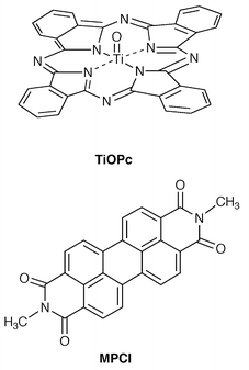
The effect of fullerene (C60) doping on photoelectric conversion was investigated. A new triple-layer cell, ITO/MPCI/C60-doped TiOPc/TiOPc/Au, exhibited a higher quantum yield for charge-carrier photogeneration (ϕ = 0.34 for 720 nm monochromatic light) than the double-layer cell without the C60-doped TiOPc layer, ITO/MPCI/TiOPc/Au, upon irradiation with monochromatic light which TiOPc mainly absorbs. The higher quantum yield for charge-carrier photogeneration upon irradiation particularly with light which TiOPc mainly absorbs may be attributed to efficient charge separation by successive electron transfer from the C60 anion radical, generated by photoinduced electron transfer from TiOPc to C60 in the C60-doped TiOPc layer, to MPCI. The triple-layer cell showed a high conversion efficiency of 0.63% for incident white light at an intensity of ca. 94 mW cm−2.134
4 Oligothiophenes with well-defined structures
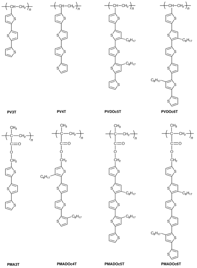
Oligothiophenes with well-defined structures have recently received a great deal of attention not only as model compounds for electrically conducting polythiophenes but also as a new class of organic π-electron systems. A number of unsubstituted and substituted oligothiophenes have been synthesized136,137 and their molecular and crystal structures,138,139 as well as optical,140,141 electrochemical,142,143 and electrical properties144–153 have been studied.We have investigated the synthesis and electrical and photoelectric properties of new oligothiophenes with varying conjugation lengths.150–153 In addition, we have created novel families of amorphous molecular materials containing the oligothiophene moiety,44–47,118,122 a novel class of gel-forming compounds containing the oligothiophene moiety,154 and a series of novel polymers containing pendant oligothiophenes.
4.1 Electrical conductivities of electrochemically oxidised oligothiophenes
With regard to electrical conductivities of oligothiophenes, both charge-transfer complexes and chemically-oxidised salts have been reported. We have investigated electrical conductivities of a series of electrochemically oxidised oligothiophenes with varying conjugation lengths.150–153 Electrochemical oxidation is of interest in that it produces definite ion-radical salts with one component of the supporting electrolyte as a dopant. The compounds studied include α-ethyl-disubstituted quaterthiophene (DEt4T), quinquethiophene (DEt5T), sexithiophene with two octyl groups at the β-position (DEtDOc6T), and septithiophene with two octyl groups at the β-position (DEtDOc7T), and β-octyl-substituted thiophene nonamer (6Oc9T), decamer (4Oc10T), and dodecamer (4Oc12T).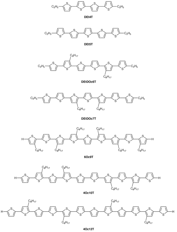
The anodic oxidations of DEt4T, DEt5T, DEtDOc6T, and DEtDOc7T were reversible owing to the presence of the ethyl groups at the α-position of each terminal thiophene ring, which prevents the coupling reaction of resulting cation radicals. Oligothiophenes with longer π-conjugation lengths, e.g., 6Oc9T, 4Oc10T, and 4Oc12T, hardly undergo coupling reaction of the resulting cation radicals. While the second oxidation process of DEt4T is irreversible, those of DEt5T and the oligothiophenes with longer π-conjugation lengths are reversible.150 It is of interest to note that the difference between the 1st and 2nd oxidation potentials becomes progressively smaller with increasing conjugation length and that only one anodic and the corresponding cathodic waves which involve two electron oxidation and reduction are observed with regard to 4Oc10T and 4Oc12T.152 Controlled-potential anodic oxidation of each dichloromethane solution of DEt4T and DEt6T at the peak potential produced black powders as precipitates in the solution. The electrochemical oxidations of DEtDOc7T, 6Oc9T, 4Oc10T, and 4Oc12T were carried out using vacuum-deposited or spin-coated films on the ITO electrode. Table 5 summarises room-temperature conductivities of solid cation radicals together with activation energies for electrical conduction. It was found that electrical conductivity significantly increases with increasing conjugation length of oligothiophenes. The room-temperature conductivity of electrochemically-oxidised 4Oc12T was 10 S cm−1, which is eight orders of magnitude greater than that of DEt4T (9 × 10⁻⁸ S cm-1).152
| Compound | E1/2ox/Va | Degree of doping (mol%) | Conductivity/S cm−1 | Activation energy/eV |
|---|---|---|---|---|
| avs. Ag/Ag+ (0.01 mol cm−3). bTwo-electron oxidation. cMeasured by a two-probe d.c. method for pellets. dMeasured by a four-probe d.c. method for films. | ||||
| DEt4T | 0.58 | ∼100 | 9 × 10⁻⁸c | 0.54 |
| DEtDOc6T | 0.46 | ∼100 | 3 × 10⁻⁵c | 0.20 |
| DEtDOc7T | 0.42 | ∼100 | 2 × 10⁻²d | 0.15 |
| 6Oc9T | 0.48 | ∼100 | 4 × 10⁻¹d | 0.07 |
| 4Oc10T | 0.43b | ∼200 | 3d | 0.07 |
| 4Oc12T | 0.36b | ∼200 | 10d | 0.05 |
4.2 Photovoltaic properties of oligothiophenes
p–n Heterojunction devices using thin films of septithiophene (7T) and octithiophene (8T) as p-type organic semiconductors and PV as an n-type organic semiconductor were fabricated and their performances examined.155 The power conversion efficiencies of the devices, ITO/PV(300 Å)/7T(500 Å)/Au and ITO/PV(400 Å)/8T(300 Å)/Au, were ca. 0.2 and 0.6%, respectively, for incident white light at 10–200 mW cm−2. It is shown that oligothiophenes, e.g., heptamer and octamer, constitute a new class of promising materials that function as p-type semiconductors for use in photovoltaic devices.5 Non-conjugated polymers containing pendant π-electron systems
Linear π-conjugated polymers are not only known as electrically conductive materials but also have recently been found to function as electrochromic,14,156 photovoltaic,8–10 and organic EL device materials.157,158Non-conjugated polymers containing pendant π-electron systems are also of interest for the following reasons; the variety of possible pendant molecules, chemical stability, ease of processability, photoconductivity of pendant π-electron systems, and invariance of the standard redox potential with the degree of doping. When these polymers are used as electrode materials for secondary batteries, a flat voltage during discharge is expected to be maintained owing to the invariance of the standard oxidation/reduction potentials of these polymers with the degree of doping. Photoconductivity coupled with semiconductivity resulting from electrochemical doping may lead to application of doped polymers as photoactive materials for photovoltaic devices. Non-conjugated polymers containing pendant π-electron systems may undergo clear colour change on electrochemical doping and dedoping.
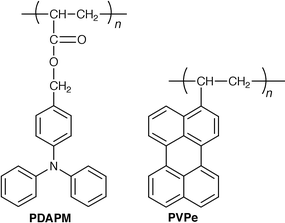
We have studied the synthesis and electrochemical doping of non-conjugated vinyl and methacrylate polymers containing pendant π-electron systems, and investigated the electrical, photovoltaic, and electrochromic properties of doped polymers.159,160 Application of non-conjugated polymers as electrode materials for lithium secondary batteries has also been studied.161,162 The polymers studied include poly(N-vinylcarbazole) (PVCz), poly(3,6-dibromo-N-vinylcarbazole) (PDBrVCz), poly(2-N-carbazolylethyl vinyl ether) (PCEVE), poly(N-glycidylcarbazole) (PGCz), poly(vinylferrocene), poly[4-(diphenylamino)phenylmethyl methacrylate] (PDAPM), poly(1-vinylpyrene) (PVPy), poly(3-vinylperylene) (PVPe), 1∶1 alternating copolymers containing N-vinylcarbazole as one component,163–166 and a novel class of vinyl and methacrylate polymers containing pendant oligothiophenes with varying conjugation length, PV3T, PV4T, PVDOc5T, PVDOc6T, PMA3T, PMADOc4T, PMADOc5T, and PMADOc6T.167–176 In particular, the novel class of polymers containing pendant oligothiophenes are expected to have unique properties characteristic of both the non-conjugated backbone and the π-conjugated linear oligomers. It is of interest to examine the correlation between the length of pendant π-conjugated linear oligomers and electrical and electrochromic properties of the resulting electrochemically doped polymers.
5.1 Alternating copolymers as new electron-beam resist materials
Certain 1∶1 alternating copolymers, e.g., poly(olefin-alt-SO2), have found successful application as positive electron-beam resists.We have designed and synthesized a new class of 1∶1 alternating copolymers of N-vinylcarbazole (VCz) and allylglycidyl fumarate (AGF) or ethylglycidyl fumarate (EGF).The alternating copolymers, poly(VCz-alt-AGF) and poly(VCz-alt-EGF), which contain alternately cross-linking epoxy or epoxy and allyl groups and a dry-etch resistant carbazole moiety as pendant groups, function as dry-etch resistant, negative electron-beam resists.163–165
Poly(VCz-alt-AGF) and poly(VCz-alt-EGF) obtained at the equimolar monomer feed ratio at 50°C had number-average molecular weights of 80000 and 60000, molecular weight distributions of 4.3 and 1.8, and relatively high Tgs of 130 and 140°C, respectively. They formed good films on a silicon wafer by spin coating.
Both copolymers were found to function as negative electron-beam resists on exposure to a 20 keV electron beam. Poly(VCz-alt-AGF) enabled the fabrication of ca. 0.2 µm line width and 1 µm spacing with vertical sidewalls. The sensitivity was as high as 2.5 µC cm−2.165
5.2 Electrochemical doping of non-conjugated pendant polymers
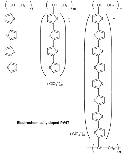
Electrochemical doping of non-conjugated pendant polymers was carried out by controlled-potential anodic oxidation in the presence of tetrabutylammonium perchlorate as a supporting electrolyte using the following methods; (1) electrolysis of polymer films coated on the electrode in acetonitrile, (2) electrodeposition of doped polymer films from dichloromethane solution of polymers, and (3) electrolytic polymerisation of vinyl monomers in dichloromethane with concurrent deposition of doped polymer films onto the electrode.159The electrochemically doped polymers were identified as partially oxidised radical cation salts containing ClO4− as a dopant. The infrared absorption spectra and cyclic voltammograms indicate that the electrochemically doped polymers containing pendant carbazole and triphenylamine moieties are partially cross-linked at the 3-position of the carbazole ring and at the para-position of the phenyl ring in the triphenylamine moiety due to the coupling reactions of the pendant carbazole and triphenylamine cation radicals. Polymers containing pendant oligothiophenes, e.g., PV3T and PV4T, undergo cross-linking at the α-position of the terminal thiophene ring.
5.3 Photovoltaic properties of doped polymers
We have studied photovoltaic properties of electrochemically doped polymers such as PVCz and PDAPM, both of which act as p-type semiconductors with photoconducting properties. The use of such electrochemically doped polymers is of interest in the following points. (1) The bulk resistivity is decreased. (2) The species involved in the formation of the depletion layer at the interface are clear. That is, the charge carriers, i.e., the radical cations of the pendant molecules accept electrons at the interface. (3) The use of doped polymer–dye systems enables both expansion of the spectral response to the visible or near infrared region and attainment of a higher quantum efficiency for photogeneration of charge carriers.159Schottky type devices were fabricated by sandwiching the electrochemically doped polymer film between the semitransparent aluminium and gold or ITO electrodes. The dyes used are perylene or anthanthrone pigment. The cell showed rectification behavior in the dark. A Schottky barrier is formed at the interface between aluminium and the electrochemically doped polymer which act as a p-type semiconductor. The cell using 0.5 µm thick electrochemically doped PDAPM film doped with N,N′-bis(3,5-dimethylphenyl)-3,4∶9,10-perylenebis(dicarboximide) (XPCI) exhibited conversion efficiencies of 2.8% for the transmitted monochromatic light of 470 nm (incident photon power: 1.3 mW cm−2).
5.4 Electrochromic properties of polymers containing pendant oligothiophenes
We have synthesized novel classes of vinyl and methacrylate polymers containing pendant oligothiophenes with varying conjugation lengths and studied their electrical and electrochromic properties.167–176 It was expected that they would exhibit clear colour changes on electrochemical doping and dedoping, owing to the well-defined structures of the pendant oligothiophenes, and that the colour could be controlled by varying the length of the oligothiophenes. These polymer films were found to undergo reversible, clear colour change on electrochemical oxidation and reduction. For example, the colour switches from blue to pale yellow and from green to yellow for PV3T and PV4T, respectively. When the cycle of doping and dedoping for each 2 s was repeated over 500 times, reversible, clear colour change took place. The response times for colouration and decolouration were ca. 4.8 and 0.3 s for PVDOc6T. Novel methacrylate copolymers containing pendant terthiophene and oligo(ethylene oxide) moieties, poly[(2,2′∶5′,2″-terthiophen-5-yl)methyl methacrylate-co-α-ethoxy-ω-methacryloyloligo(ethylene oxide)] (poly(MA3T-co-MAEO)), prepared by radical copolymerisation of the corresponding monomers, were also found to undergo reversible, clear colour change from yellowish orange to purple and vice versa on electrochemical doping and dedoping. The response time for colour change on electrochemical doping and dedoping was found to be shorter for the copolymers than for the corresponding methacrylate homopolymer containing pendant terthiophene (PMA3T). Non-conjugated polymers containing pendant oligothiophenes constitute a novel class of electrochromic materials.Acknowledgements
The author thanks all the coauthors of the publications cited in this article. Financial support of the following grants is greatly appreciated: Grant-in-Aid for Scientific Research on New Program (05NP0301), Grant-in-Aid for Scientific Research on Priority Area Research (04205094 and 06239243) and JSPS Research for the Future Program (JSPS-RFTF-97P-00104) from the Ministry of Education, Science and Culture of Japan.References
- M. Pope, H. P. Kallmann and P. Magnante, J. Chem. Phys., 1963, 38, 2042 CrossRef CAS
.
- C. W. Tang and S. A. Van Slyke, Appl. Phys. Lett., 1987, 51, 913 CrossRef CAS
- J. H. Burroughes, D. D. C. Bradley, A. R. Brown, R. N. Marks, K. Mackay, R. H. Friend, P. L. Burn and A. B. Holmes, Nature, 1990, 347, 539 CrossRef CAS
- C. W. Tang, S. A. Van Slyke and C. H. Chen, J. Appl. Phys., 1989, 65, 3610 CrossRef CAS
- B. O'Regan and M. Grätzel, Nature, 1991, 353, 737 CrossRef CAS
- M. K. Nazeeruddin, A. Kay, I. Roddicio, R. Humphry, E. Müller, P. Liska, N. Vlachopoulos and M. Grätzel, J. Am. Chem. Soc., 1993, 115, 6382 CrossRef CAS
- U. Bach, D. Lupo, P. Comte, J. E. Moser, F. Weissörtel, J. Salbeck, H. Spreitzer and M. Grätzel, Nature, 1998, 395, 583 CrossRef
- G. Yu and A. J. Heeger, J. Appl. Phys., 1995, 78, 4510 CrossRef CAS
- J. J. M. Halls, C. A. Walsh, N. C. Greenham, E. A. Marseglia, R. H. Friend, A. C. Moratti and A. B. Holmes, Nature, 1995, 376, 498 CrossRef CAS
- G. Yu, J. Gao, J. C. Hummelen, F. Wudl and A. J. Heeger, Science, 1995, 270, 1789 CrossRef CAS
- P. M. S. MonkR. J. MortimerD. R. Rosseinsky, Electrochromism: Fundamentals and Applications, VCH, Weinheim, 1995. Search PubMed
- A. Kumar, D. M. Welsh, M. C. Morvant, F. Piroux, K. A. Abboud and J. R. Reynolds, Chem. Mater., 1998, 19, 896 CrossRef CAS
- J. D. Debad and A. J. Bard, J. Am. Chem. Soc., 1998, 120, 2476 CrossRef CAS
- S. A. Sapp, G. A. Sotzing and J. R. Reynolds, Chem. Mater., 1998, 10, 2101 CrossRef CAS
- D. L. Meeker, D. S. K. Mudigonda, J. M. Osborn, D. C. Loveday and J. P. Ferraris, Macromolecules, 1998, 31, 2943 CrossRef CAS
- Y. Lis, J. Hagen and D. Haarer, Synth. Met., 1998, 94, 273 CrossRef
- Y. Maruyama and N. Iwasaki, Chem. Phys. Lett., 1974, 24, 26 CrossRef CAS
- D. J. Plazek and J. H. Magill, J. Chem. Phys., 1966, 45, 3038 CrossRef CAS
- R. J. Greet and D. Turnbull, J. Chem. Phys., 1966, 46, 1243 CrossRef
- Y. Shirota, T. Kobata and N. Noma, Chem. Lett., 1989, 1145 CAS
- W. Ishikawa, H. Inada, H. Nakano and Y. Shirota, Chem. Lett., 1991, 1731 CAS
- T. OharaN. FujiiY. Shirota, 76th Annual Meeting of the Chemical Society of Japan, Kanagawa, 1999, prepr. no. 1, p. 372. Search PubMed
- H. Inada and Y. Shirota, J. Mater. Chem., 1993, 3, 319 RSC
- A. Higuchi, H. Inada, T. Kobata and Y. Shirota, Adv. Mater., 1991, 3, 549 CrossRef CAS
- W. Ishikawa, H. Inada, H. Nakano and Y. Shirota, Mol. Cryst. Liq. Cryst., 1992, 211, 431 Search PubMed
- W. Ishikawa, K. Noguchi, Y. Kuwabara and Y. Shirota, Adv. Mater., 1993, 5, 559 CrossRef CAS
- Y. Kuwabara, H. Ogawa, H. Inada, N. Noma and Y. Shirota, Adv. Mater., 1994, 6, 677 CAS
- E. Ueta, H. Nakano and Y. Shirota, Chem. Lett., 1994, 2397 CAS
- A. Higuchi and Y. Shirota, Mol. Cryst. Liq. Cryst., 1994, 242, 127 Search PubMed
- H. Kageyama, K. Itano, W. Ishikawa and Y. Shirota, J. Mater. Chem., 1996, 6, 675 RSC
- A. Higuchi, K. Katsuma and Y. Shirota, Kobunshi Ronbunshu, 1996, 53, 829 Search PubMed
- H. Ogawa, H. Inada and Y. Shirota, Macromol. Symp., 1997, 125, 171 Search PubMed
- Y. Shirota, Y. Kuwabara, D. Okuda, R. Okuda, H. Ogawa, H. Inada, T. Wakimoto, H. Nakada, Y. Yonemoto, S. Kawami and K. Imai, J. Lumin., 1997, 72–74, 985 CrossRef CAS
- K. Katsuma and Y. Shirota, Adv. Mater., 1998, 10, 223 CrossRef CAS
- H. Nakano, E. Ueta and Y. Shirota, Mol. Cryst. Liq. Cryst., 1998, 313, 241 Search PubMed
- Y. ShirotaK. OkumotoH. Inada, Synth. Met., in the press. Search PubMed
- E. UetaM. NomuraW. IshikawaH. NakanoY. Shirota, to be submitted for publication.
- A. N. Sobolev, V. K. Belsky, J. P. Romm, N. Yu. Chernikova and E. N. Guryanova, Acta Crystallogr., Sect. C, 1985, 41, 967 CrossRef
- Y. C. Lin and D. E. Williams, Acta. Crystallogr., Sect. B, 1975, 31, 318 CrossRef
- H. Inada, K. Ohnishi, S. Nomura, A. Higuchi, H. Nakano and Y. Shirota, J. Mater. Chem., 1994, 4, 171 RSC
- J. Sakai, H. Kageyama, S. Nomura, H. Nakano and Y. Shirota, Mol. Cryst. Liq. Cryst., 1997, 296, 445 Search PubMed
- A. Higuchi, K. Ohnishi, S. Nomura, H. Inada and Y. Shirota, J. Mater. Chem., 1992, 2, 1109 RSC
- H. Kageyama, K. Ohnishi, S. Nomura and Y. Shirota, Chem. Phys. Lett., 1997, 277, 137 CrossRef CAS
- T. Noda, I. Imae, N. Noma and Y. Shirota, Adv. Mater., 1997, 9, 239 CrossRef CAS
- T. Noda, H. Ogawa, N. Noma and Y. Shirota, Adv. Mater., 1997, 9, 720 CrossRef CAS
- T. Noda and Y. Shirota, J. Am. Chem. Soc., 1998, 120, 9714 CrossRef CAS
- T. Noda, H. Ogawa, N. Noma and Y. Shirota, J. Mater. Chem., 1999, 9, 2177 RSC
- S. YoshikawaY. KotaniY. Shirota, 69th Annual Meeting of the Chemical Society of Japan, Kyoto, 1995, prepr. no. 2, p. 641. Search PubMed
- T. Ujike, K. Moriwaki, H. Nakano and Y. Shirota, J. Photopolym. Sci. Technol., 1998, 11, 33 Search PubMed
- Y. Shirota, K. Moriwaki, S. Yoshikawa, T. Ujike and H. Nakano, J. Mater. Chem., 1998, 8, 2579 RSC
- D. Nagahama, T. Ujike, K. Moriwaki, S. Yoshikawa, H. Nakano and Y. Shirota, J. Photopolym. Sci. Technol., 1999, 12, 277 Search PubMed
- K. Nishimura, T. Kobata, H. Inada and Y. Shirota, J. Mater. Chem., 1991, 1, 897 RSC
- M. Yoshiiwa, H. Kageyama, F. Wakaya, M. Takai, K. Gamo and Y. Shirota, J. Photopolym. Sci. Technol., 1996, 9, 57 Search PubMed
- M. Yoshiiwa, H. Kageyama, Y. Shirota, F. Wakaya, K. Gamo and M. Takai, Appl. Phys. Lett., 1996, 69, 2605 CrossRef CAS
- T. Kadota, H. Kageyama, F. Wakaya, K. Gamo and Y. Shirota, J. Photopolym. Sci. Technol., 1998, 11, 147 Search PubMed
- T. Kadota, H. Kageyama, F. Wakaya, K. Gamo and Y. Shirota, J. Photopolym. Sci. Technol., 1999, 12, 375 Search PubMed
- K. OkumotoK. WayakuT. NodaH. KageyamaY. Shirota, Synth. Met., in the press. Search PubMed
- J. Bettenhausen and P. Strohriegl, Adv. Mater., 1996, 8, 507 CAS
- J. Bettenhausen, M. Greczmiel, M. Jandle and P. Strohriegl, Synth. Met., 1997, 91, 223 CrossRef CAS
- M. Jandke, P. Strohriegl, S. Berleb, E. Werner and W. Brütting, Macromolecules, 1998, 31, 6434 CrossRef CAS
- J. Salbeck, N. Yu, J. Bauer, F. Weissörtel and H. Bestgen, Synth. Met., 1997, 91, 209 CrossRef CAS
- J. Salbeck, F. Weissörtel and J. Bauer, Macromol. Symp., 1997, 125, 121 Search PubMed
- P.-W. Wang, Y.-J. Liu, C. Devadoss, P. Bharathi and J. S. Moore, Adv. Mater., 1996, 8, 237 CAS
- J. Luie and J. F. Hartwig, J. Am. Chem. Soc., 1997, 119, 11695
-
(a) K. Naito and A. Miura, J. Phys. Chem., 1993, 97, 6240 CrossRef CAS
- W. Ishikawa, H. Inada, H. Nakano and Y. Shirota, J. Phys. D: Appl. Phys., 1993, 26, B94 Search PubMed
- J. Liu, Q. Deng and Y. C. Jean, Macromolecules, 1993, 26, 7149 CrossRef CAS
- M. Kusumoto, Y. Shirota and Y. Itoh, Polym. Prep. Jpn., 1998, 47, 350 Search PubMed
- M. KusumotoY. ShirotaY. Itoh, 74th Annual Meeting of the Chemical Society of Japan, Kyoto, 1998, prepr. no. 1, p. 491. Search PubMed
- H. Nakano, K. Akamatsu, K. Moriwaki and Y. Shirota, Chem. Lett., 1996, 701 CAS
- M. Kusumoto, K. Moriwaki, H. Nakano and Y. Shirota, J. Photopolym. Sci. Technol., 1998, 11, 29 Search PubMed
- K. Moriwaki, M. Kusumoto, K. Akamatsu, H. Nakano and Y. Shirota, J. Mater. Chem., 1998, 8, 2671 RSC
- W. D. Gill, J. Appl. Phys., 1972, 43, 5033 CrossRef
- D. Emin, Electronic and Structural Properties of Amorphous Semiconductors, ch. 7, ed. P. G. Le Comber and J. Mort, Academic Press, New York, 1973. Search PubMed
- L. B. Schein and J. X. Mack, Chem. Phys. Lett., 1988, 149, 109 CrossRef CAS
- H. Bässler, Phys. Status Solidi B, 1981, 107, 9
- H. Bässler, Phys. Status Solidi B, 1993, 175, 15 CrossRef
- T. Sasakawa, T. Ikeda and S. Tazuke, J. Appl. Phys., 1989, 65, 2750 CrossRef CAS
- P. M. Borsenberger, J. Appl. Phys., 1990, 68, 5188 CrossRef CAS
- P. M. Borsenberger, E. H. Magin and J. J. Fitzgerald, J. Phys. Chem., 1993, 97, 8250 CrossRef CAS
-
(a) Y. Shirota, S. Nomura and H. Kageyama, Proc. SPIE Int. Soc. Opt. Eng., 1998, 3476, 132 Search PubMed
- K. Nishimura, H. Inada, T. Kobata, Y. Matsui and Y. Shirota, Mol. Cryst. Liq. Cryst., 1992, 217, 235 Search PubMed
- S. Nomura, K. Nishimura and Y. Shirota, Mol. Cryst. Liq. Cryst., 1994, 253, 79 Search PubMed
- S. Nomura, K. Nishimura and Y. Shirota, Thin Solid Films, 1996, 273, 27 CrossRef CAS
- S. Nomura and Y. Shirota, Chem. Phys. Lett., 1997, 268, 461 CrossRef CAS
- S. Nomura, K. Nishimura and Y. Shirota, Mol. Cryst. Liq. Cryst., 1998, 313, 247 Search PubMed
- S. Nomura and Y. Shirota, Mol. Cryst. Liq. Cryst., 1998, 315, 217 Search PubMed
- C. Giebeler, H. Antoniadis, D. D. C. Bradley and Y. Shirota, Appl. Phys. Lett., 1998, 72, 2448 CrossRef CAS
- C. Giebeler, H. Antoniadis, D. D. C. Bradley and Y. Shirota, J. Appl. Phys., 1999, 85, 608 CrossRef CAS
- H. KageyamaH. OhishiY. Shirota, to be submitted for publication.
- S. NomuraH. KageyamaY. Shirota, 76th Annual Meeting of the Chemical Society of Japan, Kanagawa, 1999, prepr. no. 1, p. 402. Search PubMed
- M. van der Auweraer, F. C. De Schryver, P. M. Borsenberger and J. J. Fitzgerald, J. Phys. Chem., 1993, 97, 8808 CrossRef CAS
- S. Heun and P. M. Borsenberger, Chem. Phys., 1995, 200, 245 CrossRef CAS
- P. M. Borsenberger, E. H. Magin and J. Shi, Physica B, 1996, 217, 212 CrossRef CAS
- J. A. Sinicropi, J. R. Cowdery-Corvan, E. H. Magin and P. M. Borsenberger, Chem. Phys., 1997, 218, 331 CrossRef CAS
- R. G. Kepler, P. M. Beeson, S. J. Jacobs, R. A. Anderson, M. B. Sinclair, V. S. Valencia and P. A. Cahill, Appl. Phys. Lett., 1995, 66, 3618 CrossRef CAS
- M. Redecker, D. D. C. Bradley, M. Jandke and P. Strohriegl, Appl. Phys. Lett., 1999, 75, 109 CrossRef CAS
-
(a) Photochromism, Molecules and Systems, ed. H. Dürr, H. Bouas-Laurant, Elsevier, Amsterdam, 1990 Search PubMed
- G. M. Wallraff and W. D. Hinsberg, Chem. Rev., 1999, 99, 1801 CrossRef CAS
- J. Fujita, Y. Ohnishi, Y. Ochiai and S. Matsui, Appl. Phys. Lett., 1996, 68, 1297 CrossRef CAS
- N. FujiiK. KatsumaY. Shirota, 76th Annual Meeting of the Chemical Society of Japan, Kanagawa, 1999, prepr. no. 1, p. 373. Search PubMed
- M. KinoshitaT. NodaY. Shirota, 76th Annual Meeting of the Chemical Society of Japan, Kanagawa, 1999, prepr. no. 1, p. 373. Search PubMed
-
(a) Y. Shirota, Proc. SPIE Int. Soc. Opt. Eng., 1997, 3148, 186 Search PubMed
- Y. ShirotaT. NodaH. Ogawa, Proc. SPIE Int. Soc. Opt. Eng., 1999, 3797, in the press. Search PubMed
- S. A. Van Slyke, C. H. Chen and C. W. Tang, Appl. Phys. Lett., 1996, 69, 2160 CrossRef CAS
- D. F. O'Brien, P. E. Burrows, S. R. Forrest, B. E. Koene, D. E. Loy and M. E. Thompson, Adv. Mater., 1998, 10, 1108 CrossRef CAS
- K. Itano, T. Tsuzuki, H. Ogawa, S. Appleyard, M. R. Willis and Y. Shirota, IEEE Trans. Electron Devices, 1997, 44, 1218 CrossRef CAS
- Y. Shirota, Y. Kuwabara, H. Inada, T. Wakimoto, H. Nakada, Y. Yonemoto, S. Kawami and K. Imai, Appl. Phys. Lett., 1994, 65, 807 CrossRef CAS
- H. Murata, C. D. Merrit, H. Inada, Y. Shirota and Z. Kafafi, Appl. Phys. Lett., 1999, 75, 3252 CrossRef CAS
- Y. Hamada, C. Adachi, T. Tsutsui and S. Saito, Jpn. J. Appl. Phys., 1992, 31, 1812 CAS
- J. Kido, C. Ohtaki, K. Hongawa and K. Nagai, Jpn. J. Appl. Phys., 1993, 32, L917 CAS
- K. Tamao, M. Uchida, T. Izumizawa, K. Furukawa and S. Yamaguchi, J. Am. Chem. Soc., 1996, 118, 11974 CrossRef CAS
- M. KinoshitaY. Shirota, to be submitted for publication.
- C. Hosokawa, H. Higashi, H. Nakamura and T. Kusumoto, Appl. Phys. Lett., 1995, 67, 3853 CrossRef CAS
- J. Kido, M. Kimura and K. Nagai, Chem. Lett., 1996, 47 CAS
- H. Ogawa, K. Ohnishi and Y. Shirota, Synth. Met., 1997, 91, 243 CrossRef CAS
- H. OgawaT. NodaY. Shirota, J. Soc. Inf. Disp., in the press. Search PubMed
- T. Noda, H. Ogawa and Y. Shirota, Adv. Mater., 1999, 11, 283 CrossRef CAS
- T. NodaY. Shirota, J. Lumin., in the press. Search PubMed
- F. Geiger, M. Stoldt, H. Schweizer, P. Bäuerle and E. Umbach, Adv. Mater., 1993, 5, 922 CAS
- G. Horowitz, P. Delannoy, H. Bouchriha, F. Deloffre, J.-L. Fave, F. Garnier, R. Hajlaoui, M. Heyman, F. Kouki, P. Valat, V. Wintgens and A. Yassar, Adv. Mater., 1994, 6, 752 CrossRef CAS
- T. Noda, H. Ogawa, N. Noma and Y. Shirota, Appl. Phys. Lett., 1997, 70, 699 CrossRef CAS
- H. Ogawa, R. Okuda and Y. Shirota, Appl. Phys. A., 1998, 67, 599 CrossRef
- H. Ogawa, R. Okuda and Y. Shirota, Mol. Cryst. Liq. Cryst., 1998, 315, 489 Search PubMed
- K. Itano, H. Ogawa and Y. Shirota, Appl. Phys. Lett., 1998, 72, 636 CrossRef CAS
- K. OkumotoY. Shirota, J. Lumin., in the press. Search PubMed
-
(a) M. HanackH. HeckmannR. Polley, ‘Phthalocyanins and related compounds', in Houben-Weyl, Methods Org. Chem., Suppl. Vol. E9d, Thieme, Stuttgart, 1997, p. 717 Search PubMed
- S. Kera, A. Abduaini, M. Aoki, K. Okudaira, N. Ueno, Y. Harada, Y. Shirota and T. Tsuzuki, Thin Solid Films, 1998, 327–329, 278 CrossRef CAS
- S. Kera, A. Abduaini, M. Aoki, K. Okudaira, N. Ueno, Y. Harada, Y. Shirota and T. Tsuzuki, J. Electron Spectrosc. Relat. Phenom., 1998, 88–91, 885 CrossRef CAS
- C. W. Tang, Appl. Phys. Lett., 1986, 48, 183 CrossRef CAS
- N. Hirota, N. Noma, Y. Shirota, K. Iuchi and H. Miyazaki, Kobunshi Ronbunshu, 1990, 47, 839 Search PubMed
- T. Tsuzuki, N. Hirota, N. Noma and Y. Shirota, Thin Solid Films, 1996, 273, 177 CrossRef CAS
- T. Tsuzuki, Y. Kuwabara, N. Noma, Y. Shirota and M. R. Willis, Jpn. J. Appl. Phys., 1996, 35, L447 CrossRef CAS
- T. TsuzukiY. ShirotaJ. RostalskiD. Meissner, Solar Energy Mater. Solar Cells, in the press. Search PubMed
- T. Saito, W. Sisk, T. Kobayashi, S. Suzuki and T. Iwayanagi, J. Phys. Chem., 1993, 97, 8026 CrossRef CAS
- J. Nakayama, T. Konishi and M. Hoshino, Heterocycles, 1988, 27, 1731 Search PubMed
- P. Bäuerle, T. Fischer, B. Bidlingmeier, A. Stabel and J. P. Rabe, Angew. Chem., Int. Ed. Engl., 1995, 34, 303 CrossRef
- S. Hotta and K. Waragai, Adv. Mater., 1993, 6, 896
- D. Fichou, B. Bachet, F. Demanze, I. Billy, G. Horowitz and F. Garnier, Adv. Mater., 1996, 8, 500 CAS
- J. W. Sease and L. Zechmeister, J. Am. Chem. Soc., 1947, 69, 270 CrossRef CAS
- J. M. Tour and R. Wu, Macromolecules, 1992, 25, 1901 CrossRef CAS
- J. Guay, P. Kasai, A. Diaz, R. Wu, J. M. Tour and L. H. Dao, Chem. Mater., 1992, 4, 1097 CrossRef CAS
- P. Bäuerle, U. Segelbaher, A. Maister and M. Mehring, J. Am. Chem. Soc., 1993, 115, 10217
- D. Fichou, G. Horowitz, B. Xu and F. Gariner, Synth. Met., 1990, 39, 243 CrossRef CAS
- E. E. Havinga, I. Rotte, E. W. Meijer, W. ten Hoeve and H. Wynberg, Synth. Met., 1991, 41–43, 473 CrossRef
- S. Hotta and K. Waragai, J. Mater. Chem., 1991, 1, 853 Search PubMed
- A. Abderrahim, D. Didier, H. Mohamed, B. Nessak, G. Horrowitz and F. Garnier, Adv. Mater., 1992, 4, 490
- Y. Matsuura, Y. Oshima, Y. Misaki, H. Fujiwara, K. Tanaka, T. Yamabe and S. Hotta, Synth. Met., 1996, 82, 155 CrossRef CAS
- D. D. Graf, J. P. Campbell, L. L. Miller and K. R. Mann, J. Am. Chem. Soc., 1996, 118, 5480 CrossRef CAS
- N. Noma, K. Kawaguchi, I. Imae, H. Nakano and Y. Shirota, J. Mater. Chem., 1996, 6, 117 RSC
- N. Noma, K. Kawaguchi, I. Imae and Y. Shirota, Synth. Met., 1997, 84, 597 CrossRef CAS
- S. Funaoka, I. Imae, N. Noma and Y. Shirota, Synth. Met., 1999, 101, 600 CrossRef CAS
- Y. ShirotaN. NomaS. FunaokaH. YamaguchiH. Kawamoto, to be submitted for publication.
- P. LiuY. ShirotaY. Osada, Polym. Adv. Tech., in contribution. Search PubMed
- N. Noma, T. Tsuzuki and Y. Shirota, Adv. Mater., 1995, 7, 647 CrossRef CAS
- F. Garnier, G. Tourillon, M. Gazard and J. C. Dubois, J. Electrochem. Anal. Chem., 1983, 148, 299 Search PubMed
-
(a) A. Kraft, A. C. Grimsdale and A. B. Holmes, Angew. Chem., Int. Ed., 1998, 37, 402 CrossRef
- R. H. Friend, R. W. Gymer, A. B. Holmes, J. H. Burroughes, R. N. Marks, C. Taliani, D. D. C. Bradley, D. A. Dos Santos, J. L. Brédas, M. Lögdlund and W. R. Salaneck, Nature, 1999, 397, 121 CrossRef CAS
-
(a) Y. Shirota, N. Noma, Y. Shimizu, H. Kanega, I.-R. Jeon, K. Nawa, T. Kakuta, H. Yasui and K. Namba, Synth. Met., 1991, 41–43, 3031 CrossRef
- Y. Shirota, in New Functional Materials, Vol. C, ed. T. Tsuruta, M. Doyama and M. Seno, Elsevier Science Publishers B.V., 1993, p. 377 and references cited therein. Search PubMed
- Y. Shirota, T. Nogami, N. Noma, T. Kakuta and H. Saito, Synth. Met., 1991, 41–43, 1169 CrossRef
- I.-R. Jeon, N. Noma and Y. Shirota, Bull. Chem. Soc. Jpn., 1992, 65, 1062 CAS
- W. Zeng, Y. Shirota, M. Endo and Y. Tani, Chem. Lett., 1989, 1013 CAS
- W. Zeng, Y. Yoneda and Y. Shirota, J. Photopolym. Sci. Technol., 1989, 2, 57 Search PubMed
- Y. Shirota, Y. Yoneda, W. Zeng, H. Kawada and K. Murata, J. Photopolym. Sci. Technol., 1990, 3, 165 Search PubMed
- Y. Shirota, Y. Matsumoto, T. Tanaka, N. Noma, K. Seki, H. Yamamoto and H. Inokuchi, Mol. Cryst. Liq. Cryst., 1990, 183, 227 Search PubMed
- K. Nawa, K. Miyawaki, I. Imae, N. Noma and Y. Shirota, J. Mater. Chem., 1993, 3, 113 RSC
- K. Nawa, K. Miyawaki, I. Imae, N. Noma and Y. Shirota, Synth. Met., 1993, 55–57, 1176 CrossRef
- Y. Shirota, N. Noma, K. Namba, K. Nawa and I. Imae, Trans. Mater. Res. Soc. Jpn., 1994, 15A, 309 Search PubMed
- K. Nawa, I. Imae, N. Noma and Y. Shirota, Macromolecules, 1995, 28, 723 CrossRef CAS
- I. Imae, K. Moriwaki, N. Noma and Y. Shirota, Synth. Met., 1995, 69, 285 CrossRef CAS
- Y. Ohsedo, I. Imae, N. Noma and Y. Shirota, Synth. Met., 1996, 81, 157 CrossRef CAS
- I. Imae, K. Nawa, Y. Ohsedo, N. Noma and Y. Shirota, Macromolecules, 1997, 30, 380 CrossRef CAS
- I. Imae, N. Noma and Y. Shirota, Synth. Met., 1997, 85, 1385 CrossRef CAS
- Y. Ohsedo, I. Imae and Y. Shirota, Synth. Met., 1999, 103, 969 CrossRef
- Y. OhsedoI. ImaeY. Shirota, Electrochim. Acta, in the press. Search PubMed
Footnote |
| † Basis of a presentation given at Materials Chemistry Discussion No. 2, 13–15 September 1999, University of Nottingham, UK. |
| This journal is © The Royal Society of Chemistry 2000 |