Influence of discharge parameters on the resolution of depth profiling by pulsed glow discharge atomic emission spectrometry
Chenglong Yang, Kris Ingeneri, Matt Mohill and W. W. Harrison*
Department of Chemistry, University of Florida, Gainesville, FL 32611-7200, USA
First published on UnassignedUnassigned7th January 2000
Abstract
Investigations have been performed using microsecond pulsed glow discharge atomic emission spectrometry (GD-AES) to determine the effect of the glow discharge parameters, including applied pulse voltage, pulse width, pulse frequency and gas pressure, on the resolution of depth profiling. The results indicate that a concave crater profile is obtained for low voltage, whereas the curvature is convex for high voltage. The criteria of a flat crater bottom and good depth resolution are fulfilled only with a limited range of voltages at each operating pressure. The results also imply that the pulse frequency and pulse width have little effect on the resolution of depth profiling; thus a wide dynamic range of layers from several nanometers to tens of micrometers can be analyzed by increasing or decreasing the pulse frequency and width. Under the optimized parameters, a thin coating of Cu (50 nm) on steel, an electroplated steel and a computer hard-disk with multiple thin layers were analyzed.
Introduction
Glow discharge atomic emission spectrometry (GD-AES) is well known as a useful technique for the bulk analysis of solid samples.1 In this regard, we have used a microsecond pulsed Grimm glow discharge2 to achieve several analytical advantages, including enhanced sputtering rate and emission intensity, compared with dc. It has also proven to be an excellent tool for depth profile analysis due to precise control over the sample removal rate with short duration, repetitive pulses to strip atoms from a thin film.3 Each pulse removes only a fraction of a layer, such that thin films of only a few atomic distances can be removed over a period of several hundred pulses.Quantitative depth profiling depends on the sample material being removed uniformly layer by layer across the area exposed to sputtering by argon ions and fast atoms.4,5 Under actual working conditions, this is never fully realized. The formation of crater curvature by non-uniform erosion and of sample roughness by sputter-induced effects tends to degrade the measured intensity versus time curves and consequently decreases the accuracy of the quantitative measurement of film thickness. For any given material, the resultant crater shape is expected to be a function of the operating parameters, including the applied voltage and discharge gas pressure. The influence of the operating parameters on the crater shape has been described in several papers for dc glow discharge5–8 and radiofrequency (rf) glow discharge.9 However, a pulsed Grimm glow discharge shows some significant deviations from the characteristics of a dc glow discharge.2 The pulse width and pulse frequency can play an important role in controlling the sputtering rate. Therefore, appropriate operating parameters, unique to the pulsed discharge, must be chosen to obtain the best resolution for depth profiling.
In this study, the discharge parameters, including the applied pulse voltage, pulse width, pulse frequency and argon gas pressure of a microsecond pulsed GD-AES, were evaluated with regard to the crater shape and the resolution of depth profiling. Layer samples from 50 nm to tens of micrometers with multiple thin layers were measured under the optimized parameters.
Experimental section
A standard Grimm GD source, supplied by LECO Corp., St. Joseph, MI, USA, was employed in conjunction with a high voltage pulsed power supply (Model 350, Velonex, Santa Clara, CA, USA). The modified LECO SA-2000 surface analyzer for pulsed Grimm GD-AES has been described in detail elsewhere.2,3 The pulse width and frequency of the pulsed power supply were varied from 0.1 to 300 µs and from 1 to 100![[thin space (1/6-em)]](https://www.rsc.org/images/entities/char_2009.gif) 000 Hz, respectively. Voltages up to 3000 V were applied to the GD source. A sync output from the pulsed power supply was used to trigger the boxcars in order to synchronize the firing of the discharge and signal collection.
000 Hz, respectively. Voltages up to 3000 V were applied to the GD source. A sync output from the pulsed power supply was used to trigger the boxcars in order to synchronize the firing of the discharge and signal collection.The signal readout and data handling system of the LECO spectrometer were changed to accommodate the microsecond pulsed signals.3 The signals from the preamplifier, as well as the discharge voltage and current, were monitored simultaneously with a digital oscilloscope (Hewlett Packard 54542C, Palo Alto, CA, USA). The output signals were temporally gated for detection and processed with individual boxcar integrators (SR250, Stanford Research Systems, Sunnyvale, CA, USA). The signals from the boxcars were then sent to a computer via an analog-to-digital (A/D) converter (SR245, Stanford Research Systems). A schematic diagram of the microsecond pulsed Grimm GD-AES system is illustrated in Fig. 1. The character and preparation of the samples used are detailed in a separate publication.3
 | ||
| Fig. 1 Schematic diagram of pulsed Grimm GD spectrometer for depth profiles. | ||
Results and discussion
When monitoring depth profiles by emission intensities, the transition between two layers is clearly evidenced by the disappearance of the signal resulting from the top layer and the emergence of the signal from the lower layer. We have demonstrated that the time to the signal crossing point between these layers is linear with depth and reproducible (within 5%),3 indicating that merely measuring the time of the crossing point is a crude but effective means of determining the depth of a layer, with appropriate standards. This method, however, does not take into consideration the shape of the transitions between the layers. When dealing with layers of unknown thickness or with the resolution of successive layers on a substrate, the resolution (measured by the sharpness of the slope between layers) will become increasingly important.An ideal depth profiling method would remove sample material uniformly layer by layer, effecting a sharp transition between the two layers and creating a crater profile with steep sides and a flat bottom. In practice, glow discharge sputtering processes suffer from non-uniform plasmas, irregular surface formations and sputtered atom redeposition that reduce the distinction between layers. Therefore, time–intensity profiles have a definite slope in the transition region between layers, as shown in Fig. 2 for a commercial layer sample of Zn and Ni on Fe. The selection of optimum experimental conditions that sharpen the time–intensity profiles will enhance the depth resolution.
 | ||
| Fig. 2 Depth resolution ΔZ, reported as the difference in x-axis (time) at 84% and 16% of the maximum intensity. The sample is Zn on steel (Zn-20454, Kocour Co., Chicago, IL, USA). | ||
Much work has been done to quantify the depth resolution based on the slopes of the time–intensity profiles. It might be helpful to revisit some of the equations used to describe the resolution.3,10 The depth resolution (ΔZ) is defined as
 | (1) |
 | (2) |
 | (3) |
The predominant effects that limit the depth resolution of GD-AES are the curvature of the crater bottom and its relative roughness. Clearly, if the sample erosion plane is not flat, it will tend to intersect two different elemental layers over some time scale that will negatively impact on the resolution. Even if the erosion plane is flat, surface structures variously referred to as cones, spires or hillocks will produce a broadened effective layer of exposure to the discharge.6
For a given sample material, the resulting crater shape is determined by the discharge parameters (voltage, current or power, discharge gas and its pressure). Therefore, it is important to find the appropriate operating parameters that yield uniform sample erosion and the flattest crater bottom. The electrical operating parameters of the GD lamp are not independent of one another. If one parameter is altered (e.g. voltage), the others (current and power) are determined as a function of the discharge gas pressure and the sample composition. A key consideration in maintaining a constant sputter yield is the energy of the bombarding gas ions, in this case argon. The discharge voltage determines the electric field across the cathode dark space, which in turn sets the acceleration voltage of the argon ions onto the sample surface. It is important that the voltage remains constant, so the pulse power supply for the GD is operated in a constant voltage mode.
The pulse voltage at constant pressure is the means of controlling the discharge power and therefore an important parameter determining the crater shape and depth resolution. The magnitude of the constant voltage has been reported to affect the crater profiles in dc discharges, so it was necessary to determine the optimum value for the pulse discharge.11Fig. 3(a–c) shows the effects of three different operation powers on the crater profiles. The respective peak discharge settings were: (a) a low power regime of 100 W (800 V, 0.12 A, 3 Torr Ar pressure); (b) a medium power regime of 270 W (1200 V, 0.22 A, 4 Torr argon); and (c) a high power regime of 680 W (2000 V, 0.35 A, 3 Torr argon). The sputtering times of the three trials were varied slightly to allow them to be sputtered to the same depth.
 | ||
| Fig. 3 Crater profiles for different operating conditions (computer hard-disk): (a) 100 W; (b) 270 W; (c) 680 W. | ||
As shown in Fig. 3, for low power (voltage), a concave crater profile is obtained, whereas high power results in a convex curvature. Only a mid-range of pulse voltage yields a relatively flat crater bottom. For example, the optimum pulse voltage is between 1200 V and 1400 V for a 3 Torr argon gas discharge. This same trend between power and crater shape was observed with a dc discharge,5 and, in general, the pulsed discharge corresponds to the dc results, except that the range of voltages is higher in the pulsed mode.
One possible explanation for this effect suggests that the crater shape results from the electric field focusing or defocusing the bombarding ions responsible for sputtering.5,12 At low pulse power, the sputter area becomes larger than that at higher powers, and also produces a crater with a concave bottom. With increasing voltage, a different type of asymmetrical sputtering occurs, resulting in a convex crater shape. At moderate powers, the uniform current distribution is nearly perpendicular to the cathode surface. Experimentally, it is the moderate power regime which results in the flat, uniform crater shapes and, as expected, the best depth resolution.
The effect of pulse voltage
The effect of increasing pulse voltage on the intensity–time profiles is shown in Fig. 4 for the Cr layer of a computer hard-disk, analyzed at a discharge pressure of 4 Torr. For clarity, the emission intensities have been normalized to emphasize the effect of voltage on sputtering. The temporal profile for 800 V in Fig. 4 clearly lacks sharp transitions on the rising and falling edges. Crater profiles obtained as a function of voltage indicate that, at low pulse voltage (e.g. 800 V), a concave crater is obtained. This would indicate that, at low voltage, the underlying layer is exposed first at the central portion of the crater. Fig. 5(a) is a magnified digital image of a sputter pattern of a copper layer on steel at low voltage (800 V, 3 Torr, 10 µs pulse width, 200 Hz). The image has been digitally altered to enhance the contrast between the copper and steel layers. The black circular region in Fig. 5(a) marks the edge of the deep sputter erosion area. The dark surface represents the copper top layer, whereas the lighter center region indicates the steel layer. The lower power conditions correspond to a concave crater shape and also yield a lower emission intensity due to a lower sputtering rate. At high pulse voltages (e.g. 2000 V), the sputtering rate and emission intensity are increased. However, the crater shape shows the underlying layer to be exposed asymmetrically at the edge of the crater first. Fig. 5(b) is a digital image of a sputter region at 1800 V under the same conditions as in Fig. 5(a). A contribution from the underlying layer is observed early, while significant amounts of the top layer are still present in the center of the discharge area. This extends the signal overlap of the two layers, rather than obtaining the desired sharp transition. Observing the sample crater under a simple optical microscope, the contrast between Cu and Fe layers can be clearly followed as a function of discharge conditions. Since both high and low voltage discharges produce higher sputtering in one localized region and reduced sputtering in another, the signals from each are correspondingly unsatisfactory. The cause of poor depth resolution is the non-uniform erosion under very high or very low operating power. | ||
| Fig. 4 The intensity–time profiles of a Cr layer in a computer hard-disk sample using different pulse voltages at 4 Torr argon pressure. | ||
 | ||
| Fig. 5 Digitally enhanced images of burn spots for a copper layer on a steel substrate: (a) low voltage at 800 V; (b) high voltage at 1800 V. | ||
A 250 nm Cu layer on a steel substrate was used to investigate the relative depth resolution (ΔZ/d) of increasing applied pulse voltage at different argon gas pressures. Fig. 6 summarizes the results of this study. At each pressure, there is an optimum operating pulse voltage to obtain the best resolution. Recall that a low ΔZ/d value represents the best resolution. The effect of voltage is clearly influenced by the selected pressure. At 3 and 4 Torr, voltage effects are small, but the best resolution is still obtained at mid-level voltages. At higher pressures, low voltage is essential to obtain the best resolution.
 | ||
| Fig. 6 Effect of the applied pulse voltage on the relative depth resolution for a 250 nm Cu layer on a steel substrate at different pressures. | ||
The effect of argon gas pressure
The gas pressure is an essential parameter influencing the depth resolution in the glow discharge, because it not only determines the discharge current under conditions of constant pulse voltage, but also the atomic mean free paths, the energy of ions bombarding the cathode surface and the extent of analyte redeposition, which may also influence the resolution.9 The effect of pressure on the intensity–time profiles of a Cr layer in a hard-disk is shown in Fig. 7. The discharge voltage was held at 1200 V, while the argon gas pressure was varied from 2 to 6 Torr. The corresponding discharge current was varied between 0.14 and 0.46 Å. The results show that increasing the gas pressure at constant voltage increases the sputtering rate by increasing the current, and therefore the layer interface is reached earlier. Unlike the voltage study, the slope of the increasing emission signal does not change with respect to pressure. At gas pressures beyond 4.5 Torr, the sputtering penetrates each new layer at the edge of the crater first, resulting in a convex crater, similar to that seen in Fig. 5(b). At these higher pressures, redeposition is also expected to increase because of the shorter mean free path. The redeposition rate is greater at high pressure, which causes an effective reduction of the net sputtering rate. The greatest reduction of local sputtering rate takes place in the center of the crater, while the edge of the burn spot is less affected.8 It is therefore more difficult to obtain a flat crater shape at high pressures. | ||
| Fig. 7 The intensity–time profiles of a Cr layer in a hard-disk sample with different pressures at a pulse voltage of 1200 V. | ||
The relative depth resolution as a function of pressure at pulse voltages of 1200 and 1400 V is shown in Fig. 8. The results indicate that the depth resolution at low pressure is better than that at high pressure due to non-uniform erosion at higher pressures. The best depth resolution can be achieved at 3 or 4 Torr with pulse voltages of 1400 or 1200 V, respectively.
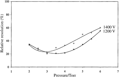 | ||
| Fig. 8 Effect of operating pressure on relative depth resolution for a 250 nm Cu layer on a steel substrate at voltages of 1200 and 1400 V. | ||
The effect of pulse width and pulse frequency
Prior work has shown the effect of pulse frequency and pulse width in pulsed GD-AES.3 The pulse frequency does not affect the sputtering rate and emission intensity of each pulse, which is as expected since each pulse is identical. However, changing the pulse width presents a modified pulse configuration that could affect analytical signals. The peak emission intensity remains constant with pulse width, because the pulse voltage is fixed. From increasing pulse width, one would expect a longer lasting emission signal, with a linear effect on the sputtered material lost, but this does not happen. The sputter ablation per pulse shows a non-linear increase when the pulse width is increased, because the effective discharge pulse is not sustained linearly with the pulse width.Under conditions of constant pulse voltage and gas pressure, the crater shapes do not change with different pulse widths and frequencies. The effects of these two parameters on a 250 nm Cu layer on a steel substrate are shown in Fig. 9. The results show that depth resolutions at different pulse widths and frequencies are essentially constant under the conditions used. From an analytical standpoint, by holding the pulse voltage and gas pressure constant, the pulse width and frequency can be used as adjustment variables to achieve suitable ablation rates for the desired thickness of the layer samples at hand, and neither factor will affect the depth resolution. For very thin layers, fine control of the sputter process may be particularly useful.
 | ||
| Fig. 9 Effect of pulse width (A) and pulse frequency (B) on the relative depth resolution for a 250 nm Cu layer on a steel substrate at different conditions: (a) 1200 V, 4 Torr, 200 Hz; (b) 1400 V, 3 Torr, 10 µs pulse width. | ||
Applications
Having determined the optimal conditions for obtaining a flat crater profile, several samples have been chosen to illustrate the effectiveness of the pulsed Grimm glow discharge source. Its main advantage lies in its ability to increase or decrease the sputtering rate without altering the depth resolution. Because of the reduced duty cycle of the pulsed source, less material can be removed per unit time. Due to the increased operating power possible during the short duration pulse, no loss in signal intensity is obtained. Actually, increases in signal and sensitivity have been shown even though less material is removed. This allows thin layers to be analyzed. However, the pulsed technique is not limited to analyzing only thin layers. By increasing the frequency, higher sputter rates may be obtained as required for thicker layers.Thick layer samples
A 6 µm Zn–Ni (11.7% Ni and 88.3% Zn) coating on a low-alloy cold rolled steel substrate (Sollac Steel, France)1 was used to demonstrate the ability to analyze relatively thick layers. Fig. 10 shows the time profile of this analysis, normalizing the elemental intensities by the adjustment of detector voltages. The discharge conditions used were 4 Torr argon and 1200 V. In order to minimize the analysis time, the pulse width and frequency were set to 50 µs and 1000 Hz respectively. The typical reproducibility of transition times to the layer interface is approximately 3%.3 The depth resolution under these conditions is about 1.5 µm. | ||
| Fig. 10 Analysis of a thick Zn–Ni layer (6 µm) on a steel substrate at the optimized conditions of 1200 V pulse voltage, 4 Torr pressure, 1000 Hz pulse frequency and 50 µs pulse width. | ||
Thin layer samples
Standardized, certified thin layer samples are difficult to obtain commercially, so samples consisting of a 50 nm layer of Cu were prepared on a steel substrate using the thermal evaporation capabilities of the Department of Material Science, University of Florida (VE-400, Veeco Instruments Inc., Plainview, NY, USA). The layer depth was verified by a piezoelectric crystal in the evaporation chamber. Considering the depth of the thin layer, a lower frequency (200 Hz) was used during this analysis. Fig. 11 shows the time versus intensity profiles of the thin layer sample analyzed with operating conditions of 4 Torr argon, 1200 V and 10 µs pulse width. The results show that about 60 s are required to sputter away the 50 nm Cu layer, which provides sufficient time for reliable data acquisition. The depth resolution is about 10 nm. | ||
| Fig. 11 Analysis of a thin Cu layer (50 nm) on a steel substrate at the optimized conditions of 1200 V pulse voltage, 4 Torr pressure, 200 Hz pulse frequency and 10 µs pulse width. | ||
Multilayer samples
An interesting and readily available source of multilayer sample materials is found in computer hard-drives which have crashed and been replaced in personal computers. While information from the manufacturers is difficult to obtain, given the proprietary nature of disk composition, the layers may be identified, as shown in Fig. 12. The conditions of the discharge were optimized as previously described. The pulse frequency was 600 Hz and the pulse width 10 µs. Phosphorus shows up in the Co layer and again as a major component in the base Ni–P composition.13 To obtain depth measurements, the sputter rates of individual elements under these conditions are needed, and these measurements are currently under study. | ||
| Fig. 12 Analysis of the layers of a computer hard-disk (Quantum) at the optimized conditions of 1200 V pulse voltage, 4 Torr pressure, 600 Hz pulse frequency and 10 µs pulse width. | ||
Conclusions
Pulsed Grimm glow discharge atomic emission spectrometry has been proven to be an effective technique for depth profile analysis. The results indicate that pulse voltage and gas pressure, rather than pulse width and pulse frequency, are the dominant parameters that determine the formation of the crater shape and depth resolution. Given the appropriate choice of operating parameters, the technique can be effectively used for depth profiling analysis of layer samples from several nanometers to tens of micrometers with good depth resolution. Future work will include quantifying depth resolution under optimized operating conditions, allowing quantitative depth analysis to be performed.Acknowledgements
This research was supported by the Department of Energy, Basic Energy Sciences and LECO Corporation. The authors thank Dr. J. D. Winefordner and Dr. B. W. Smith for helpful discussions. They also acknowledge Dr. P. Holloway from the Department of Material Science for sample preparation and Dr. Arne Bengtson from the Swedish Institute for Metals Research for supplying samples.References
- A. Bengtson, Spectrochim. Acta, Part B, 1994, 49, 411 CrossRef.
- C. L. Yang, K. Ingeneri and W. W. Harrison, J. Anal. At. Spectrom., 1999, 14, 693 RSC.
- C. L. YangK. IngeneriM. MohillW. W. Harrison, Anal. Chem., accepted for publication. Search PubMed.
- A. Bengtson, A. Eklund, M. Lundholm and A. Saric, J. Anal. At. Spectrom., 1990, 5, 563 RSC.
- N. Jakubowski and D. Stuewer, J. Anal. At. Spectrom., 1992, 7, 951 RSC.
- A. Quentmeier, J. Anal. At. Spectrom., 1994, 9, 355 RSC.
- A. Raith, R. C. Hutton and J. C. Huneke, J. Anal. At. Spectrom., 1993, 8, 867 RSC.
- E. Rose and P. Mayr, Mikrochim. Acta, 1989, 1, 197 CAS.
- M. Parker, M. L. Hartenstein and R. K. Marcus, Anal Chem., 1996, 68, 4213 CrossRef CAS.
- F. Prabler, V. Hoffmann, J. Schumann and K. Wetzig, J. Anal. At. Spectrom., 1995, 10, 677 RSC.
- Glow Discharge Spectroscopies, ed. R. K. Marcus, Plenum Press, New York, 1996, p. 340. Search PubMed.
- A. Bogaerts and R. Gijbels, Spectrochim. Acta, Part B, 1997, 52, 765 CAS.
- J. E. Williams Jr. and C. Davison, J. Electrochem. Soc., 1990, 137, 3260.
| This journal is © The Royal Society of Chemistry 2000 |