The influence of operational modes on sputtering rates and emission processes for different sample matrices in rf-GD-OES
Covadonga Péreza, Rosario Pereiroa, Nerea Bordelb and Alfredo Sanz-Medela
aDepartment of Physical and Analytical Chemistry, Faculty of Chemistry,, University of Oviedo, 33006, Oviedo, Spain. E-mail: asm@sauron.quimica.uniovi.es
bDepartment of Physics, University of Oviedo, 33007, Oviedo, Spain
First published on UnassignedUnassigned7th January 2000
Abstract
A study was carried out to select the most convenient pair of the three key interdependent plasma operating parameters in a radiofrequency glow discharge (rf-GD) (generator output power, dc-bias developed in the sample surface and pressure) to be fixed in order to measure intensities by optical emission spectrometry (OES) or sputtering rates with adequate precision. The best operating conditions in order to obtain values of emission yields unaffected by the nature of the sample matrix are also given. Three different modes of rf-GD-OES operation were studied and emission intensities of selected elements (Fe, Ni, Zn, Cu) in eight different matrices were measured. Results showed that a mode in which generator output power and dc-bias voltage are fixed while pressure is allowed to vary provided the worst relative standard deviations (RSDs) for the emission intensities measured (higher than 15%). The other two approaches studied (either generator output power and pressure fixed with the dc-bias varied or pressure and dc-bias voltage fixed with the generator output power varied) provided better performance (lower than 4%) in both cases. Concerning the sputtering rates, the two modes, working either with variable dc-bias or with variable power, gave good precision for three replicates. Finally, these two modes seemed also to provide reliable values for the emission yields of each analyte emission line under study in the different reference samples investigated. Comparison of results observed by keeping constant the pressure in a rf-GD and those achieved by dc-GD in its usual mode of operation (variable pressure, maintaining fixed the voltage and current) shows similar behaviour for both sources when comparing the trends followed by the emission yields when modifying the matrix.
Introduction
There is a clear revival of glow discharge (GD) spectrometry applied to the rapid depth profiling and bulk analysis of solid materials. GDs can be generated with direct current (dc) and radiofrequency (rf) power. The overwhelming majority of depth profile work to date has been done with dc sources, because rf systems have only become commercially available in the last few years. However, rf-GDs are demonstrating excellent performance characteristics for the bulk analysis of both insulating and conducting samples.1–5A few methods have been successfully evaluated so far for quantitative depth profiling using the well established dc-GDs with optical emission spectrometry (OES) detection. Probably, the most popular quantification model in dc-GD-OES is the method developed by Bengtson6 which has been implemented with minor modifications in most of the commercially available GD instruments. Bengtson's model allows analytical quantification, regardless of the GD operating conditions, since the measured intensities of the analytical lines are corrected as a function of the modifications in current and voltage throughout the analysis.
Also, simple procedures for quantification in “in depth profile analysis" based on the emission yield concept, Rλ, which can be defined as the emitted light per unit sputtered mass of an element, have been developed by Pons-Corbeau and co-workers7,8 and by Takimoto et al.9 In both methods, the voltage and the current in the discharge are considered parameters producing important effects on the emission yield,10 but it is matrix-independent to a first approximation. Successful quantifications following these methods seem to be achieved. In fact, quantification according to the Japanese method has been realized in software and is commercially available.
Concerning the rf-GD source,11 no method has been thoroughly evaluated so far for quantitative depth-profiling with this source. In 1993, Payling and Jones12 presented a method to separate the contributions of the three key variables of the discharge (current, voltage and pressure) in a direct current source and proposed a quantitative approach in which the emission yield was assumed to depend only on pressure. This theory was shown to be valid for the rf-GD mode as well.13
Recently, Parker et al.14 presented a study of the role of GD parameters (power and pressure) on the emission yields obtained for rf-GD-OES. In their work, it was observed that, for a given sample, rf power produces small changes in the emission yields while slight changes in pressure affect more significantly the emission yields. Similar results were achieved by Bengtson and Hänström15 for both types of discharge (dc and rf); however, they have also reported that, for different matrices, the emission yields for a given emission line reached similar values when the pressure was modified (in this case the electrical parameters were kept constant). On the other hand, Payling16 has presented a study in which the emission yields for five elements in five different matrices were evaluated; he established that the emission yield depended on the current, voltage and pressure.
The aim of this paper was to evaluate which pair of parameters out of the three key parameters: power, dc-bias voltage or pressure, are the most convenient to be fixed in order to obtain a better reproducibility both for the sputtering rates of several samples with different matrices and for the emission intensities of the selected spectral lines of the elements under study (Fe, Ni, Zn and Cu) with rf-GD-OES. Also, emission yields were measured and the influence of the operation mode on the results was investigated and compared with previous results obtained in our laboratory using dc-GD-OES.
Experimental
A diagram of the experimental set-up employed in the development of rf-GD-OES in our laboratory has been given elsewhere.17 Therefore, only a brief description will be given here. The GD chamber, made of stainless steel, was constructed according to the design of Marcus and co-workers.3 A limiting disc with a central orifice of 3 mm id was used to restrict the area of the cathode (sample) being sputtered. The anode–cathode distance was 0.24 mm. The optical measurements with the dc-GD were carried out with the detector described in previous work.17 In the experiment performed here with rf-GD the detector employed was a charge-coupled device (CCD) from Princeton Instruments (Model LN/CCD-1100-PF/UV) cooled by liquid nitrogen.The dc-bias voltages developed in the rf-GD were measured using a digital real-time oscilloscope from Tektronix, Model TDS 340 A-100 MHz. The operation of the oscilloscope did not give rise to any noticeable modification, either in the working conditions of the GD or in the analytical performance.
Table 1 lists the reference materials used as cathodes (with a flat-disc shape) in this work with the concentrations of the selected elements under study. All the reference materials were polished to a mirror-finish using metallographic grinding paper (120, 240 and 400 grit) and then cleaned with methanol prior to the analysis. The cathodes were first sputter-cleaned for 100 s to ensure a reproducible atomisation surface and then the emission intensities of each studied element under the selected working conditions were collected.
| Material | Reference | Company | Fe | Ni | Zn | Cu |
|---|---|---|---|---|---|---|
| Pure Iron | B.S. 50D | Brammer Std. Co. | 99.96 | — | — | — |
| Aust. Stainless steel | 13X-12535-BB | MBH Analytical | 61.55 | 14.88 | — | 0.08 |
| Brass | 233 | USSR certified reference material | 0.72 | 0.41 | 32.00 | 60.47 |
| Brass | 234 | USSR certified reference material | 0.99 | 1.43 | 31.10 | 61.81 |
| Al/Si | G26H2-C | MBH Analytical | 0.80 | 0.37 | 0.94 | 3.50 |
| Zinc-Base | SRM 628 | NIST | 0.07 | 0.03 | 94.30 | 0.61 |
| Brass | 31X-B7-H | MBH Analytical | 0.01 | 0.01 | 15.00 | 85.00 |
| Zn/Al/Cu | 43Z11-C | MBH Analytical | 0.18 | — | 88.00 | 0.49 |
The chosen emission spectral lines of the elements selected for this study (Fe, Ni, Zn and Cu) are shown in Table 2. Emission intensities using rf-GD were registered with an integration time of 0.03 s and a total exposure time of 3.0 s at the selected discharge conditions and two replicate measurements (burns) were taken. For dc-GD (for the comparative determination of emission yields) emission intensities were measured with an integration time of 0.02 s and a total exposure time of 3.6 s.
| Element | Wavelength/nm |
|---|---|
| Fe I | 344.1 |
| Ni I | 341.8 |
| Z II | 210.0 |
| Cu I | 296.1 |
The operating conditions selected for the rf-GD provided similar values of sputtering rates to those obtained by dc-GD at conditions of constant current (11 mA), constant voltage (690 V) and variable pressure (between 5 and 7 Torr). The selected conditions for rf-GD work were an output power of 40 W, a mean dc-bias of 460 V and a pressure of 8 Torr.
Sputtering rates, or mass loss rate during sputtering, were calculated by measuring penetration depths per unit time and considering the crater diameter and the sample density. Penetration depths of the different calibration samples were measured with a profilometer (Perth-o-meter S5P, Mahr Perthen) by measuring two profile traces in different directions across the centre of each crater. The mean of three sputtered replicates was used to calculate each penetration depth.
High-purity argon (99.999% minimum purity) from Air Liquide was employed as discharge gas.
Results and discussion
Rf-GD analysis is typically performed by fixing two key parameters: the operating pressure and the applied generator output power.12 The delivered power may differ considerably from the real power coupled to the discharge owing to power losses. It has been stated, however, that, for a given sample, these power losses are a relatively constant fraction of the total generator output power,18 whenever the pressure in the chamber is constant.A change in the pressure modifies the impedance of the rf glow space between the rf electrode and the surface grounded19 and so could produce changes in the percentage of the rf power coupled to the discharge.17 Moreover, the same power can be obtained with different values of voltage and current intensity, it being necessary to measure other parameters, viz., voltage or current intensity, in order to know the electrical conditions in the discharge. In our case, we cannot directly measure current intensity but we can measure the generator output power and the dc-bias potential developed at the smaller electrode which is the sample. In a GD, these three parameters are interrelated in such a way that, by fixing two of them, no choice as to the selection of the third is possible.20,21 Lazik and Marcus22 have shown that dc-bias values in rf-GD sources are dependent on both the power and pressure, although not to the extent seen in dc-GD sources.
Three approaches were investigated which, for simplicity during discussion, will be differentiated as detailed in Table 3, viz., method 1, 2 or 3. Table 4 shows the mean values obtained by applying methods 1, 2 and 3 to each reference material detailed therein and the relative standard deviation (RSD) of the dc-bias in method 1, the power in method 2 and the pressure in method 3 (for three replicates in each case). As can be seen, the RSD observed was higher when method 3 was adopted.
| Fixed parameters | Variable parameter | |
|---|---|---|
| Method 1 | Power: 40 W | Dc-bias |
| Pressure: 8 Torr | ||
| Method 2 | Dc-bias: 460 V | Power |
| Pressure: 8 Torr | ||
| Method 3 | Power: 40 W | Pressure |
| Dc-bias: 460 V |
| Reference material | Method 1: | Method 2: | Method 3: |
|---|---|---|---|
| Dc-bias voltage/V | Applied power/W | Pressure/Torr | |
| aReference materials used in the study of emission intensities. | |||
| B.S. 50Da | 438 ± 19 | 43 ± 1 | 6.5 ± 0.7 |
| 13X-12535-BBa | 426 ± 22 | 42 ± 2 | 6.7 ± 0.1 |
| 233 | 438 ± 1 | 42 ± 1 | — |
| 234a | 416 ± 5 | 44 ± 1 | 6.7 ± 0.4 |
| G26H2-Ca | 412 ± 16 | 46 ± 1 | 6.1 ± 0.4 |
| SRM 628 | 404 ± 3 | 51 ± 3 | — |
| 31X-B7-H | 451 ± 10 | 41 ± 1 | — |
| 43Z11-C | 394 ± 6 | 48 ± 1 | — |
Emission intensities
It is well established that in GD-OES it can be assumed that the sputtering and excitation processes are independent. Therefore, the intensity Ix of an emission line can be described by: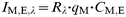 | (1) |
In each of the three methods investigated here (Table 3), emission intensities of the selected analytical lines of the different matrices were measured for each reference sample at the three discharge operating conditions indicated in Tables 3 and 4. The precision of each measurement was then calculated for three replicates.
Results showed that method 3 (variable pressure) gives the worst precision (higher than 15%) versus the other two methods (RSD lower than 4%). This observation is in agreement with results presented by Parker et al.,14 showing the notorious effect of small changes in pressure on relative emission yields while these emission yields remain virtually unaltered when modifying the applied power. As mentioned above, changes in the pressure of the chamber would give rise to noticeable modifications in the impedance of the system; therefore, the percentage of power coupled to the discharge would change17 and this fact could account for the worse precision obtained by measuring at the conditions detailed in approach 3 of Table 3.
According to eqn. (1), high imprecision in the measurement of emission intensities will also give rise to high imprecision in the calculation of emission yields. Therefore, method 3 was discarded for further experiments.
Sputtering rates
The sputtering rates of the reference materials at the selected operating conditions were obtained for methods 1 and 2 and the results observed are shown in Table 5 with the corresponding RSDs.| Sputtering rate/mg s−1 | ||
|---|---|---|
| Reference material | Method 1:40 W–8 Torr | Method 2:460 V–8 Torr |
| B.S. 50D | 0.00129 (7.5%) | 0.00166 (8.8%) |
| 13X-12535-BB | 0.00155 (1.6%) | 0.00162 (10.7%) |
| 233 | 0.00574 (2.6%) | 0.00597 (0.9%) |
| 234 | 0.00539 (8.8%) | 0.00574 (11.8%) |
| G26H2-C | 0.00076 (4.2%) | 0.00107 (5.5%) |
| SRM 628 | 0.00668 (2.2%) | 0.00865 (2.7%) |
| 31X-B7-H | 0.00545 (4.0%) | 0.00635 (3.2%) |
| 43Z11-C | 0.00547 (3.4%) | 0.00713 (3.5%) |
As can be seen in Table 5, sputtering rates were similar for both methods under investigation, since differences in discharge operating conditions were not so important. However, sputtering rates obtained by the method in which the developed dc-bias voltage was kept constant were slightly higher. This can be attributed to the higher delivered power and dc-bias developed in method 2. Table 5 also shows that the precision achieved by method 1, however, seems to be slightly better in general terms.
Emission yields
According to eqn. (1), the emission yield is given by | (2) |
Fig. 1 shows the emission yields obtained, with the rf-GD, for Ni (λ = 341.8 nm), Fe (λ = 344.1 nm), and Zn (λ = 210.0 nm); corresponding reference samples are given on the abscissa axis. For each plot, the reference materials studied are ordered according to the concentration of the element under study. As can be seen, emission yields are similar for each line regardless of the material used as cathode or the operating method selected (that is, regardless of the value of the variable parameter). Fig. 1(a) shows that the emission yield achieved for the 341.8 nm Ni line in the sample G26H2-C has a value higher (approximately a factor of 2) than those obtained with the other matrices; however, as can be observed in Table 5, the sputtering rate for G26H2-C is fairly low and so any inaccuracy in the measurement of this sputtering rate would severely affect the emission yield value. Similarly, a slightly higher emission yield is observed for the same reference material in Fig. 1(b) for the 344.1 nm Fe emission line (around a factor of 1.5). In any case, the differences in the emission yields achieved between G26H2-C and the other materials are in agreement with results presented by Bengtson and Hänström,15 who showed that, for a dc-GD at a given power and pressure, the emission yields obtained for Al matrices are 4 times higher than those measured for Cu or Fe matrices.
 | ||
| Fig. 1 Emission yields in some different reference materials with rf-GD (• Method 1, fixed 40 W–8 Torr; ○ Method 2, fixed 460V–8 Torr): (a) 341.8 nm emission line of Ni, (b) 344.1 nm emission line of Fe and (c) 210.0 nm emission line of Zn. | ||
Fig. 2 shows emission yields obtained, for comparison, using dc-GD. It is important to note here that, although the same optical equipment was used, the detector was different from that used for rf-GD, as previously indicated under Experimental. Therefore, the results with dc-GD can only be compared with rf-GD results in terms of the behaviour of emission yield trends, for the three studied lines. For these dc-GD experiments, current intensity and voltage were kept constant, while the discharge pressure was the variable parameter.
 | ||
| Fig. 2 Emission yields in some different reference materials with dc-GD (▲ 690 V–11 mA fixed): (a) 341.8 nm emission line of Ni, (b) 344.1 nm emission line of Fe and (c) 210.0 nm emission line of Zn. | ||
As can be observed in Fig. 2, emission yields obtained with dc-GD under the selected operating conditions are similar for each emission line and this corroborates previous work indicating that pressure is a parameter of minor importance in dc-GD.24 It should be highlighted that similarities in the general trends of Fig. 1 and 2 are evident, although the methodologies followed were totally different (since in method 1 for rf-GD the dc-bias varies and probably also the current intensity while in method 2 current intensity is the variable parameter). These results are in agreement with work published by Payling et al.25 comparing manganese emission yields in samples with different concentrations of analyte, by dc-GD, following three different methods: (a) fixed voltage and current intensity, (b) fixed pressure and current intensity and (c) fixed pressure and current intensity, applying in the last case corrections produced by voltage modifications. They showed that the plot of normalised emission yields gave a balanced scatter of about 1 in the three approaches.
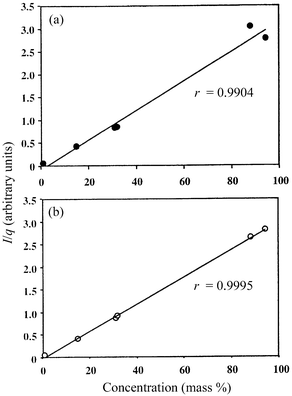
Fig. 3 and 4 show calibration graphs achieved with the two methods selected in rf-GD (Table 3), for Zn and Cu, respectively, by plotting the “emission intensity∶sputtering rate" ratio versus concentration of the analyte. As can be seen, good correlation factors are achieved for both methods, those obtained being slightly better when the dc-bias and the pressure were kept constant (method 2).
 | ||
| Fig. 3 Calibration graphs obtained with rf-GD for the 210.0 nm emission line of Zn. (a) •, Method 1 with 40 W and 8 Torr (fixed). (b) ○, Method 2 with 460 V and 8 Torr (fixed). | ||
 | ||
| Fig. 4 Calibration graphs obtained with rf-GD for the 296.1 nm emission line of Cu. (a) •, Method 1 with 40 W and 8 Torr (fixed). (b) ○, Method 2 with 460 V and 8 Torr (fixed). | ||
Conclusions
The applicability of three operational approaches to rf-GD-OES, in order to obtain emission intensities with good precision, was studied. Such approaches are based on maintaining two different fixed values of the three key variables of this discharge. The highest irreproducibility was obtained when the variable parameter was the pressure (method 3). Although we did not continue studies with this third method, because of its poor performance for emission intensity measurements, it might be of interest to investigate further its behaviour with respect to sputtering rates and emission yields achievable.The first (variable dc-bias) and second (variable power) approaches investigated here were used to measure sputtering rates of selected reference samples with different matrices. Both methods seem to provide figures of the same magnitude and a similar precision for sputtering rates.
The emission yields of emission lines for Ni, Fe and Zn, in the same reference sample, were calculated and the values obtained were again similar, independent of the reference material. In addition, the observed behaviour of rf-GD-OES was similar to that of dc-GD under commonly used operating conditions for in-depth profile analysis with this source. Moreover, calibration graphs of IM,E,λ/qMversus Zn and Cu concentrations gave good correlation factors for both rf-GD methods, particularly when the pressure and the dc-bias voltage were kept constant (method 2).
Both methods 1 and 2 deserve further study in order to assess their usefulness for in-depth profile quantification by rf-GD-OES.
Acknowledgements
Financial support from the European FEDER Programme, Project 1FD97-0444-C03, is gratefully acknowledged. Also, the authors thank Agalsa Factory (Asturias, Spain) for assistance throughout this work.References
- J. W. Coburn and E. Kay, Appl. Phys. Lett., 1971, 19, 350 CrossRef CAS.
- M. R. Winchester and R. K. Marcus, J. Anal. At. Spectrom., 1990, 5, 575 RSC.
- M. R. Winchester, C. Lazik and R. K. Marcus, Spectrochim. Acta, Part B, 1991, 46, 483 CrossRef.
- C. Lazik and R. K. Marcus, Spectrochim. Acta, Part B, 1994, 49, 649 CrossRef.
- C. Lazik and R. K. Marcus, Spectrochim. Acta, Part B, 1993, 48, 863 CrossRef.
- A. Bengtson, Spectrochim. Acta, Part B, 1994, 49, 411 CrossRef.
- J. Takadoum, J. C. Pivin, J. Pons-Corbeau, R. Berneron and J. C. Charbonnier, Surf. Interface Anal., 1984, 6, 174 CAS.
- J. Pons-Corbeau, J. P. Cazet, J. P. Moreau, R. Berneron and J. C. Charbonnier, Surf. Interface Anal., 1986, 9, 21 CAS.
- K. Takimoto, K. Nishizaka, K. Suzuki and T. Ohtsubo, Nippon Steel Tech. Rep., 1987, 33, 28 Search PubMed.
- Glow Discharge Spectroscopies, ed. R. K. Marcus, Plenum Press, New York, 1993. Search PubMed.
- D. G. Jones, R. Payling, S. A. Gower and E. Boge, J. Anal. At. Spectrom., 1994, 9, 369 RSC.
- R. Payling and D. G. Jones, Surf. Interface Anal., 1993, 20, 787 CrossRef CAS.
- R. Payling, D. G. Jones and S. A. Gower, Surf. Interface Anal., 1993, 20, 959 CrossRef CAS.
- M. Parker, M. L. Hartenstein and R. K. Marcus, Spectrochim. Acta, Part B, 1997, 52, 567 CrossRef.
- A. Bengtson and S. Hänström, J. Anal. At. Spectrom., 1998, 13, 437 RSC.
- R. Payling, Surf. Interface Anal., 1995, 23, 12 CAS.
- C. Pérez, R. Pereiro, N. Bordel and A. Sanz-Medel, Spectrochim. Acta, Part B, 1998, 53, 1541 CrossRef.
- C. M. Horwitz, J. Vac. Sci. Technol., 1983, A1, 1795 Search PubMed.
- H. R. Koenig and L. I. Maissel, IBM J. Res. Develop., 1970, 14, 168 Search PubMed.
- M. Dogan, K. Laqua and H. Massmann, Spectrochim. Acta, Part B, 1971, 26, 631 CrossRef CAS.
- R. Payling, Surf. Interface Anal., 1994, 21, 785 CrossRef CAS.
- C. Lazik and R. K. Marcus, Spectrochim. Acta, Part B, 1993, 48, 1673 CrossRef.
- J. Pons-Corbeau, Surf. Interface Anal., 1985, 7, 169 CrossRef CAS.
- A. Bengtson, A. Eklund, M. Lundholm and A. Saric, J. Anal. At. Spectrom., 1990, 5, 563 RSC.
- R. Payling, D. G. Jones and S. Gower, Surf. Interface Anal., 1995, 23, 1 CAS.
| This journal is © The Royal Society of Chemistry 2000 |