All about (N-hexadecylquinolin-4-ium-1-yl)methylidenetricyanoquinodimethanide, a unimolecular rectifier of electrical current†
Robert M. Metzger
Laboratory of Molecular Electronics, Department of Chemistry, University of Alabama, Tuscaloosa, AL 35487-0336, USA, rmetzger@bama.ua.edu
First published on UnassignedUnassigned22nd December 1999
Abstract
We found unimolecular rectification in a single molecule, (N-hexadecylquinolin-4-ium-1-yl)methylidenetricyanoquinomethanide, 1, in which the ground state is zwitterionic: D+–π–A−, and has a large dipole moment (43 D) while the first excited state is undissociated: D0–π–A0 (and has a smaller moment, between 3 and 9 D). The intervalence optical absorption band connecting these two states is strongly hypsochromic. Spectroscopic measurements (FTIR, NMR, VIS–UV, XPS) all confirm this assignment. This significant ‘first step' to unimolecular electronics, i.e. a rectifier only 2.3 nm thick, confirms a 1974 proposal by Aviram and Ratner. However, the ‘real proof' that the large current under forward bias actually travels through the molecule, has not yet been obtained.
Introduction
Milestones in unimolecular electronics
The field of unimolecular electronics started in 1974 with a proposal by Aviram and Ratner,1 that a single molecule may rectify electrical current. In the early 1980's three scientific conferences organized by the late Forrest L. Carter stirred further interest in the promise of ‘molecular electronics', that is electronic devices consisting solely of molecules.2–4By now some important milestones towards that goal have been reached:
(1) tunneling currents through aliphatic chains are larger than through aromatic chains,5
(2) the resistance of a single molecule (benzene-1,4-dithiol) bonded to two Au electrodes was measured as several MΩ (it would have been smaller, but the work function of Au and the LUMO of the molecule were mismatched, and the thiolate bonds are partially ionic),6
(3) the quantum of electrical resistance (12 kΩ) was measured at room temperature between a single carbon nanotube, glued to a conducting AFM tip, and liquid Hg,7
(4) the Aviram–Ratner mechanism,1 slightly modified, was confirmed in conductivity measurements through a monolayer of (Z)-[β-(N-hexadecylquinolin-4-ium-1-yl)-α-cyano-4-styryl]dicyanomethanide or [(N-hexadecylquinolin-4-ium-1-yl)methylidene]tricyanoquinodimethanide, C16H33–Q3CNQ, 1: this is the first proven two-terminal unimolecular electronic device.8

We review here what we have learned about the chemistry and physics of 1.8–16
The Aviram–Ratner Anzatz of unimolecular rectification
Aviram and Ratner1 proposed that a single organic molecule D–σ–A could be a rectifier of electrical current (Fig. 1). The D–σ–A ‘Gedankenmolekül', or ‘thought molecule' or ‘graphite and cellulose molecule' 2 was never synthesized, but its electronic structure illustrates the proposed rectification. The D end (tetrathiafulvalene) is a good organic one-electron donor (but poor acceptor), σ is a covalent saturated (‘sigma') bridge, and A (tetracyanoquinodimethane) is a good organic one-electron acceptor (but poor donor). The ‘Gedankenmolekül' D–σ–A, put between two metal electrodes M1 and M2, should form the rectifier M1| D–σ–A|M2, with a working thickness of 2 to 3 nm, and easy electron transfer from M2 to M1 because of the ‘downhill' through-molecule tunneling from the excited state D+–σ–A− to the ground state D0–σ–A0. There are some problems with this ‘Ansatz': the HOMOs and LUMOs of even potent organic one-electron donors and one-electron acceptors do not easily match the Fermi levels of inorganic metals; it is not easy to assemble defect-free monolayers (by Langmuir–Blodgett (LB) or by covalent ‘self-assembly' (SA) techniques), or to make reliable electrical contacts with macroscopic metal electrodes. But the challenge of making a unimolecular device was interesting (it took about 20 years). The efforts by the groups of Metzger, Panetta, Cava, Sambles, Sandman, and Ashwell to test the Aviram–Ratner ‘Ansatz' have been reviewed elsewhere.16–23 | ||
| Fig. 1 The Aviram–Ratner Ansatz, showing the through-molecule electron flow from the excited zwitterion state D+–σ–A− to the undissociated ground state D0–σ–A0. | ||
Review of work by Ashwell and Sambles
Ashwell and co-workers discovered a new class of zwitterionic molecules: a quaternary picolinium of lepidinium halide, when reacted with an alkali salt of TCNQ, can yield ground-state zwitterions; the first example was [(1-methylpyridin-1-ium-2-yl)methylidene]tricyanoquinodimethanide, P-3CNO, 3, whose crystal structure revealed that 3 was indeed a zwitterion, with a θ = 30° twist angle between the pyridinium ring and the central six-membered ring of 3CNQ.24 When made suitably amphiphilic by addition of long alkyl terminations, these zwitterions yield Z-type Langmuir–Blodgett films that are good χ(2) materials.25 For instance, 1 can be considered as a T–D+–π–A− structure, where T represents the hexadecyl ‘tail', D+ is the quinolinium ring Q, and A- is the tricyanoquinodimethanide moiety 3CNQ. 1 forms Z-type Langmuir–Blodgett multilayers with a large, resonance-enhanced χ(2)zzz = 180![[thin space (1/6-em)]](https://www.rsc.org/images/entities/char_2009.gif) pm V−1.26 It is believed that the ground state of 1 is very polar and zwitterionic, while its first excited state is less polar or undissociated, of the type T–D0–π–A0, and that the efficiency for frequency doubling, the blue color of the acetonitrile solution, and the rectification documented below, are all due to the intramolecular intervalence transfer (IVT) transition
pm V−1.26 It is believed that the ground state of 1 is very polar and zwitterionic, while its first excited state is less polar or undissociated, of the type T–D0–π–A0, and that the efficiency for frequency doubling, the blue color of the acetonitrile solution, and the rectification documented below, are all due to the intramolecular intervalence transfer (IVT) transition T–D+–π–A− → T–D0–π–A0

In 1, the quinolinium and tricyanoquinodimethanide rings may be twisted by some unknown angle θ. If θ = 0°, then the two states would be degenerate resonance states. If θ = 90° then IVT vanishes, and the blue color should disappear.
When LB multilayers of 1 were sandwiched between a noble metal electrode (Pt or Ag) and a Mg electrode (protected by an overlayer of Ag), then asymmetric currents through the laterally macroscopic multilayer indicated electrical rectification through the molecule:27
Pt|LB multilayer of 1|Mg|Ag
and even in the sandwich:
Pt|LB monolayer of 1|Mg|Ag
Doubts raised about a possible Schottky barrier at the Mg electrode|molecule interface20 prompted the insertion of an insulating monolayer of a fatty acid between the metal electrodes and three monolayers of C16H33–Q3CNQ;28I–V asymmetries were seen again, albeit between metal electrodes of very different work functions, and were ascribed to molecular rectification.28,29
Synthesis, nuclear magnetic resonance, dipole moment
The synthesis of 1 was improved, by starting from N-cetyllepidinium tosylate and a two-fold excess of Li+ TCNQ·−, in a dry DMSO solution in the presence of pyridine.8 Blue microcrystals of 1 were obtained, but they were too small and multiply twinned to yield an indexable X-ray diffractogram.8 Therefore one is reduced to suppose that, because of a definite steric hindrance, in analogy to the structure of 3, there is some unknown twist angle θ, probably somewhere between 20° and 90°, between the least-squares quinolinium and the phenyl planes of 1.The NMR spectrum of the compound8 is very diagnostic of a dipolar ground state. Since it was opined that 1 may undergo a twisted internal charge transfer (TICT) transition, maybe as a function of temperature,30 a temperature-dependent NMR study was undertaken, but no dramatic changes in the NMR spectrum were found.12
The dipole moment of a solution of 1 in CH2Cl2 was studied as a function of both temperature and concentration. After correcting for the polarization of the solvent, two estimates emerged (one from the temperature dependence of the relative permittivity, which extrapolated to about 47 D at zero concentration, the other using the Kirkwood–Fröhlich equation, which extrapolated to 40 D), whose average is 43 ± 8 D for 1 at infinite dilution in CH2Cl2: this result strongly supports the zwitterionic nature of the ground state of 1.8
Visible, near-infrared spectrum, emission spectrum
The visible–ultraviolet spectrum of 1 is solvent-dependent, particularly the long-wavelength maximum in the visible region. This maximum is at 720 nm in CH3CN, at 884 nm in CH2Cl2, and at 838 nm in CHCl3; except for CHCl3 at high concentrations, the absorbance of 1 is linear with concentration.8 The absorption and fluorescence spectra of 1 were measured at room temperature in up to eight solvents.12 The long-wavelength absorption bands have two vibronically resolved peaks in the lower-polarity solvents chloroform, dichloromethane, ethyl acetate, and tetrahydrofuran; these peaks merge into one in acetone, nitromethane, and acetonitrile. No monomer–oligomer equilibria were detected in the optical absorbance of 1 in CH2Cl2 (−5°C to 30°C), or in CH3CN (5°C to 50°C). Hence the long wavelength absorption is attributed to the monomer of 1. The short-wavelength absorption maxima do not vary monotonically with relative permittivity or index of refraction, but the long-wavelength absorption bands are strongly hypsochromic; the blue shift is almost linear with relative permittivity. This indicates that the ground state has a higher dipole moment than the electronically excited state.There are two sets of fluorescent emission lines: emissions below 600 nm, and emissions in the 1000–1400 nm region. The emissions in the near IR region are very weakly hypsochromic. That two fluorescent emissions exist for 1 is an apparent violation of Kasha's rule, which dictates that, within a set of states of the same spin multiplicity, a fluorescent emission should occur only from the lowest excited state. Other, higher excited states usually decay internally and without radiative emission, into the lowest excited state, which then emits the photon. However, if the higher-energy emission is weak (here ϕ ≈ 0.01), and is not re-absorbed, then emission from a lower-energy state becomes possible. Alternatively, molecule 1 may have different rotameric states: molecules of 1 with θ ≈ 90°, with no IVT, would emit in the visible, while molecules with a lower θ and a ‘blue' IVT will emit in the near infrared region.
An estimate of the excited state dipole moment µe can be made by comparing the absorption and fluorescent emission energies, assuming no change in the orientation of the dipole: the ratio of the energy shift between any two solvents for absorption ΔEa and for fluorescence ΔEf is ΔEa/ΔEf = μg/μe. If μg = 43 D,1 one obtains μe = 5.53 D (CHCl3–CH3CN) or μe = 2.97 D (CH2Cl2–CH3CN).12 The solvatochromism, explained by an ellipsoidal cavity model,31,32 yields an estimated excited-state dipole moment of 8.7 D.12
Theoretical calculations
A geometry-optimized PM3 calculation was performed for 1 (ΔHf = 6.02 eV). The molecule 1 is twisted; the angle between the quinolinium ring and the central phenyl ring of 3CNQ is ≈30°.8 The computed dipole moment for the ground state singlet of 1 is 10.7 D, with the highest occupied molecular orbital (HOMO) at −7.98 eV (MO # 106, localized on quinolinium, the π bridge, and the 3CNQ end) and the lowest unoccupied molecular orbital (LUMO) at −2.42 eV (MO # 107, localized on 3CNQ−); however, the bond lengths in the molecule are more quinonoid than benzenoid.8 When using a shorter alkyl chain (octyl instead of hexadecyl) and AM1, the ground state has a dipole moment of 10.56 D and ΔHf = 7.61 eV, while the excited singlet state has a smaller dipole moment, 6.36 D, and ΔHf = 10.83 eV, i.e. 3.22 eV higher.8 A PM3 calculation for the excited singlet state of 1 yielded ΔHf = 8.47 eV, a twisted geometry (θ ≈ 90°), and a high dipole moment of 45.4 D.30 The inferred approximate molecular size for 1 is 33 Å × 7 Å × 4.5 Å.8Further calculations by density functional theory, AM1, and ab initio methods15 found new conformers with high dipole moments (which increase if a solvent is included). The twist angles θ were larger than expected (Fig. 2): the ‘true' energy minimum that explains all experimental data may not yet have been found.15
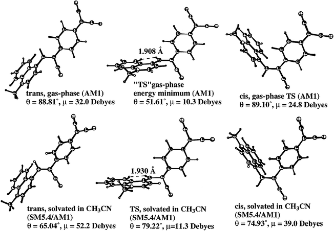 | ||
| Fig. 2 Conformational search (with and without CH3CN solvent) for high-moment energy minimum of CH3–Q3CNQ.15 | ||
Cyclic voltammogram and EPR of radical anion of 1
A cyclic voltammogram has been measured for 1, and is shown in Fig. 3. There is a one-electron quasi-reversible reduction (Ep,r = −0.545 V, Ep,o = −0.480 V, E1/2 = −0.513 V vs. SCE, ΔE = 0.065 V), and a second irreversible reduction at Ep,r = −1.16 V, and an irreversible oxidation at Ep,o = 0.49 V vs. SCE. Impurities in very small concentrations show an oxidation at 0.44 V, and reductions at Ep,r = −0.675 V and Ep,r = 0.383 V vs. SCE. Thus 1 is a reversible one-electron acceptor with electron affinity similar to that of the weak one-electron acceptor p-benzoquinone. | ||
| Fig. 3 Cyclic voltammogram of a 10−4 M solution of 1 in CH2Cl2, measured using a Pt wire working electrode, an SCE reference electrode, 0.1 M NBu4ClO4 electrolyte, N2 gas bubbled through the solution, and a scan rate of 20 mV s−1.8 | ||
A saturated solution of 1 in a 0.1 M Bu4NPF6–dimethylformamide solution, held in an electrochemical EPR cell at room temperature under Ar at −0.645 V vs. SCE, where the molecule should be reduced to its radical anion, shows the EPR spectrum shown in Fig. 4.12 This spectrum was simulated, using g = 2.0027, and isotropic hyperfine constants aN = 1.20 G (2 ×
14N, I = 1) and 2.80G (14N), aH = 1.44 G (2 ×
1H, I = 1/2), 1.80 G (2 ×
1H), and 3.0 G (1H) (Fig. 4). The coupling constants are very close to the data for the radical anion of TCNQ (aN = 1.02, aH = 1.44 G), and thus testify that most of the spin density in the radical anion of 1 is localized on the 3CNQ part of the molecule and the bridgehead proton.12
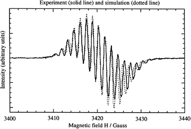 | ||
| Fig. 4 Electron paramagnetic resonance spectrum of the radical anion of 1, electrogenerated in DMF at −0.645 V vs. SCE, with 0.1 M Bu4NPF6. The simulated spectrum is shown as dashed lines.12 | ||
 | ||
| Fig. 5 Pressure–area isotherms for 1 at 14°C and 20°C, and surface (Volta or Kelvin probe) potentials at 14°C.8 | ||
Pockels–Langmuir monolayers at the air–water interface and Langmuir–Blodgett films
The Π–A isotherm of 1, measured under a green safelight, shows a collapse point at 50 Å2 molecule−1 and 34 mN m−1 (Fig. 5): this isotherm is moderately temperature-dependent.8 The 3CNO end of the molecule is clearly the hydrophilic end of the molecule; the 50 Å2 area fits the theoretical estimate for an extended conformation. The Volta potential difference ΔV is set to zero before spreading the monolayer, rises to about 0.18 V at the start of the compression, and becomes about ΔV = 0.46 V at about 120 Å2 per molecule, i.e. before the monolayer is fully compressed: the dipolar layer is more polar than, e.g. cadmium arachidate.Monolayers and multilayers of 1 were transferred as LB films at 15 mm min−1 and 20 mN m−1. Molecule 1 first transfers on the downstroke onto hydrophobic HOPG (transfer ratio 58%), but on the upstroke onto a freshly cleaned hydrophilic Au(111) single crystal and on an Al electrode (transfer ratio 90%).8 At the lower transfer speed of 15 mm min−1 the LB multilayers (past the first monolayer) are Z-type, while at the faster transfer speed of 45 mm min−1, the LB multilayers become Y-type.8 The thickness per monolayer, measured by ellipsometry (λ = 670 nm) and by surface plasmon resonance, is 22 ± 2 Å; thus, the approximate molecular axis may be tilted 48 ± 5° from the normal to the monolayer plane.8 X-Ray diffraction spectra, taken several days after film transfer onto a glass substrate, show that the Y-type films reorder to Z-type after transfer, with a thickness of 23 Å per monolayer.8
The geometry of LB multilayers of 1 on HOPG is:
HOPG|→ ← ← ← ← ← ← ← etc.
On Al it is Z-type throughout:
Al|← ← ← ← ← ← ← etc.
Here the arrow → indicates the rough molecular orientation; it points from the hexadecyl tail T and the quinolinium ring D+ (tail) towards the dicyanomethylene head of A− (arrowhead).8
A sharp and narrow absorption band peaked at 570 nm is found for LB films transferred onto a quartz substrate at 14°C in the dark, and measured at 25°C (Fig. 6). This narrow band disappears if the films are protonated, but returns when they are exposed to ammonia vapor,8 it disappears irreversibly if the films, or the solution, are exposed to bright light and air for some time.
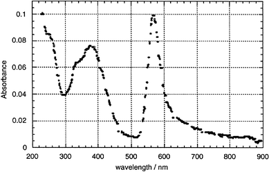 | ||
| Fig. 6 Visible spectrum of an 11-layer LB film of 1 transferred onto quartz; the narrow absorbance has a peak at 570 nm (2.17 eV; spectral width at half-maximum = 0.19 eV); the absorbance per monolayer at 633 nm is 0.0021.8 | ||
An LB monolayer of 1, transferred onto quartz, shows weak absorption maxima at 340 nm and at 565 nm. The same monolayer, excited at 350 nm, produces a clear emission peak at 492 nm, but no emission when excited at 570 nm. The absorption of 15 blue-violet LB monolayers of 1 on quartz did not change between room temperature and 77 K: this argues for no large change in the twist angle θ between these two temperatures.12
Grazing-angle Fourier transform infrared (FTIR) spectra, using p-polarized light for a monolayer of 1 on a glass substrate covered by Al (Fig. 7), show absorbances at 2850 cm−1 (symmetric C–H), 2920 cm−1 (asymmetric –CH2–), 2139 cm−1 (–C![[triple bond, length as m-dash]](https://www.rsc.org/images/entities/char_e002.gif) N) and 2175 cm−1 (–CN), indicating that the cyano groups and the methylene groups do not lie in the plane of the monolayer, but are somewhat tilted from it. The CN stretches show evidence of shifts due to partial change: negatively charged CN groups (2175 cm−1) and a shifted CN group (2135 cm−1). For a monolayer of 1 on either Au(111) or HOPG, the C–H and –CH2– signals can be seen clearly; a CN signal at 2175 cm−1 is barely visible for the monolayer on Au(111).8
N) and 2175 cm−1 (–CN), indicating that the cyano groups and the methylene groups do not lie in the plane of the monolayer, but are somewhat tilted from it. The CN stretches show evidence of shifts due to partial change: negatively charged CN groups (2175 cm−1) and a shifted CN group (2135 cm−1). For a monolayer of 1 on either Au(111) or HOPG, the C–H and –CH2– signals can be seen clearly; a CN signal at 2175 cm−1 is barely visible for the monolayer on Au(111).8
 | ||
| Fig. 7 p-Polarized grazing-angle FTIR spectrum (θ = 85°) of LB monolayer of 1 on Al.8 | ||
Fig. 8 shows the N 1s region of the XPS spectrum of 1 adsorbed on an oxide-covered Si substrate. There are three peaks, which have been fitted using standard techniques. The dominant feature at 400.5 eV is in the range for N in an organic matrix. However, there are features at higher (402.3 eV) and lower (398.8 eV) binding energies, which indicate the charge transfer state of the molecule. The lowest energy feature (398.8 eV) can be associated with nitrogen in the C≡N moiety; the highest binding energy feature (402.3 eV) is in the range associated with ammonium salts.12 This confirms that 1 is zwitterionic.12
 | ||
| Fig. 8 Nitrogen N 1s region of the X-ray photoelectron spectrum of an LB multilayer of 1 on Si. Also shown are a sloping linear background fit, Gaussian peak fits to simulate the spectrum, and the error in the fit (small circles). N 1s peaks are seen at 402.3 eV, 400.3 eV, and 398.8 eV.12 | ||
A valence band scan of a multilayer of 1 on Si (Fig. 9) reveals several peaks at binding energies 3 eV to 25 eV. These peaks can be compared with PM3/RHF calculations. The onset of the valence-band XPS at 3.7 eV on Si (−7.8 eV versus vacuum)12 agrees with the calculated HOMO at −7.98 eV.8
 | ||
| Fig. 9 Valence-band XPS spectrum of a LB multilayer of 1 on Si, with Gaussian line-fits.12 | ||
Electrical conductivity through LB films
An Edwards El 306A evaporator was used to deposit the base Al electrode and the Al pads over the LB films. The electrical conductivity was measured either with a PAR 270 potentiostat, or with a microcomputer-controlled Hewlett-Packard Model 3245A Universal Source, and a Hewlett-Packard Model 3457 A Multimeter.8 Glass or quartz or silicon substrates were first covered by 25 × 75 mm × 100 nm Al layer, next, LB monolayer or multilayer films were transferred under a green safelight, then the sample was dried for 2 days in a vacuum desiccator containing P2O5. Twelve cylindrical ‘pads' of Al (4 each of areas 2.8, 4.5, and 6.6 mm2, all either 100 nm thick or 300 nm thick, depending on the run) were finally deposited per substrate, atop the organic layer, with the substrate cooled to 77 K, to form the sandwich: ‘glass|Al|4 LB monolayers of 1|Al', or ‘glass|Al| LB monolayer of 1|Al' (Fig. 10). The multilayer results (Fig. 11) agree with the previous work,27–29 except that here the same metal (Al), with its inevitable oxide, is on both sides of the multilayer. The significant new result was that rectification was found even with a single monolayer (Fig. 12), although not all junctions were so perfect.8,14Fig. 12 shows a typical rectification curve. Above a threshold voltage Vt, the monolayer shows higher currents for positive voltage than for the corresponding negative voltage. This Vt varies from junction to junction (Vt = 0.8 to 1.3 V). The rectification ratio RR, defined by RR = (current at V0)/(current at −V0), where V0 is the highest positive bias used, ranges from 2.4 to 26.4 the first time the film is measured. But, as the cycle is repeated, RR drops steadily, and disappears after 4 to 6 cycles: under the intense electric fields, the molecular dipoles probably re-orient to minimize energy. For some of the junctions, short circuits form across the monolayer during the measurement. In the range −0.5 V to 0.5 V, the I–V curve is ohmic. In the reverse regime (negative bias), the logarithm of the current is linear with the applied bias (through-space tunneling) from −0.5 V to the highest negative bias applied (−1.5 V to −1.8 V). In the forward regime, lne(I) ∝ V for V > 0.5, up to a threshold voltage (in the range 0.8 to 1.3 V, depending on sample), above which the current rises severalfold. | ||
| Fig. 10 Orientation of the LB monolayer (a) or multilayer (b) on the glass, quartz, or Si substrate; the electrode (+) for positive bias, and the direction of ‘easy' electron flow for V > 0 are marked. In some cases Ag paste was used instead of the Ga/In eutectic.8 | ||
 | ||
| Fig. 11 Conductivity of a sandwich ‘Ga/In eutectic|Al (100 nm)|4 LB monolayers of 1 (Z-type)|Al (100 nm)|Ga/In eutectic'. Scan rate 100 mV s−1. Easier electron flow (I > 0 for V > 0) is from the bottom electrode through the film to the top electrode.8 | ||
 | ||
| Fig. 12 Rectification through a single monolayer of 1 sandwiched between Al electrodes (top Al pad area 4.5 mm2, thickness 100 nm), using Ga/In eutectic and Au wires.8 | ||
The results on both monolayers and multilayers show that the electrons preferentially flow by IVT from 3CNQ (A−) to quinolinium (D+); this is explained by modifying the AR Ansatz for the case that the ground state is zwitterionic, D+–π–A−, and the excited state is undissociated, D0–π–A0.
The junctions that do not rectify have much lower conductivities.16
Many samples, which rectified at room temperature, were measured at decreasing temperature.13 Results could easily be obtained above 250 K. Below 250 K, either open circuits or permanent or intermittent short circuits happened often: only a few reliable results were obtained below 100 K. Fig. 13 shows the I–V plot for a sample at 105 K.
 | ||
| Fig. 13 DC current I versus DC applied voltage V for a monolayer of 1 at 105 K.13 | ||
Although the barrier resistances are small for the Au|Ga/In contact, an ohmic contact resistance of about 100 kΩ was measured in a separate experiment for a non-wetting Ga/In|Al2O3|Al|Al2O3|Ga/In couple.13 Happily, this contact resistance is many orders of magnitude smaller than the resistance across the organic monolayer.13
STM Images
With a modified Nanoscope II, a monolayer of 1 deposited on HOPG yielded an image with surprising resolution (Fig. 14): this seemed to show the molecules, viewed with a Pt/Ir nanotip, seen from the dicyanomethylene end.8 The repeat area of 4.5 × 13 Å consists of a ‘light' region (closer to the nanotip) of about 4.5 × 7 Å, plus a dark region (4.5 × 6 Å). A solution drop of 1 in dimethyl sulfoxide also shows a repeat area of 4.5 Å × 13 Å.8 Using a low-current STM (Nanoscope III) an LB monolayer of 1 showed a similar image, albeit at lower resolution, with a repeat distance of 6 Å × 12 Å (Fig. 15). These images are consistent with the molecules viewed end-on, and are not graphitic. Since the monolayer coverage of 1 on HOPG is 50% or so, one seeks and finds patches on the HOPG surface where images like Fig. 15 can be seen, alternating with regions where the bare HOPG surface is seen quite clearly. | ||
| Fig. 14 STM Micrograph of Langmuir–Schaefer monolayer of 1 on HOPG, viewed with a Pt/Ir nanotip (Nanoscope II, modified to increase current 100 fold). Scan size = 2 nm × 2 nm. For details, see ref. 8. | ||
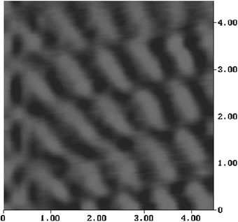 | ||
| Fig. 15 STM Image of a LB monolayer of 1 on HOPG, with Pt/Ir tip (Nanoscope III). Scan size = 4.5 nm × 4.5 nm.8 | ||
Scanning tunneling spectroscopy
Multilayers of 1 on HOPG were studied using a Pt/Ir nanotip at room temperature in air by STM and STS. Clear asymmetries in the I–V plot were seen in 15-layer films (Fig. 16), but the corresponding STM images were of a graphite superstructure. In agreement with the I–V characteristics of multilayers sandwiched between Al electrodes, the STS current is consistent with electrons flowing by intramolecular intervalence electron transfer (IVT) between LB layers 2 through 15, and with ‘jumping over' layer 1, but, as discussed above, the electrons must somehow jump between adjacent monolayers. The current must somehow also jump over the first monolayer (which is directed the ‘wrong way', and is afflicted with a poor transfer ratio).8,9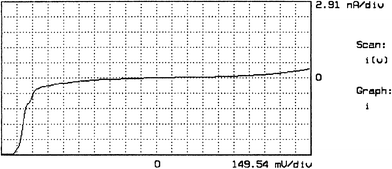 | ||
| Fig. 16 STS I–V curve for an LB film of 15 Z-type monolayers of 1 on HOPG, with Pt/Ir tip. The higher current for V < −1.35 V corresponds to electron flow from HOPG through molecules to the Pt tip.8,9 | ||
Asymmetric STS spectra are even seen for a monolayer of 1 on HOPG, and for saturated solution of 1 in DMSO over HOPG.8
Estimates of HOMO and LUMO energies
To evaluate the behavior of 1 as a unimolecular rectifier, one should inspect where the HOMO and LUMO levels are, relative to the electrode work functions ϕ: ϕ(Pt) = 5.d;7 eV, ϕ(graphite) = 4.4 eV, ϕ(Al) = 4.2 eV, and ϕ(Mg) = 3.7 eV. All voltages are below the vacuum level = 0 eV, and should be quoted as negative, but in this discussion they are quoted as positive for simplicity.Using the bias voltages ΔV measured before asymmetric conduction occurs through monolayers and multilayers on various electrodes8ELUMO = 3.0 ± 0.3 eV is estimated. This value is in rough agreement with the electron affinity of p-benzoquinone (2.4 eV), whose reduction potential in solution matches that of 1.8
The onset of valence-band XPS current,12 and a simple AM1 calculation8 both suggest EHOMO = 8 ± 0.3 eV.12 Clearly EHOMO is below the work function of most metals. Then ELUMO − EHOMO = 8.0 − 3.0 = 5 eV, which is probably large. The IVT energy is measured as only 2.17 eV in films8 and estimated to be 1.1 eV in the gas phase:12 these energies are much smaller than 5 eV, but Coulomb correlation in the D+–π–A− state and Mulliken charge-transfer mixing of states may lower the gap between the D+–π–A− and D0–π–A0 states. Clearly more calculations are needed.
Discussion
It is unfortunate that no crystal structure determination of 1 could be obtained. An estimated molecular geometry (with a θ=30° twist between the quinolinium and the phenyl rings, an extended hexadecyl ‘tail', and a 45° tilt of the long molecular axis from the normal to the monolayer plane) explains the area per molecule seen in the pressure–area isotherm, the film thickness, and the STM patterns seen in Fig. 14 and 15.8We have confirmed that 1 is not only a multilayer rectifier, but also a monolayer rectifier, by an improvement of Sambles and co-workers' original technique,27–29and in accord with a plausible modification of the Aviram–Ratner Ansatz.1 We have eliminated the uncertainty due to the previous use27,28 of two metal electrodes with different work functions.
The observed hypsochromism and large Stokes shift of the IVT fluorescence emission are consistent with the large dipole moment (43 ± 8 D) for the zwitterionic ground D+–π–A− state, and a much smaller moment (between 3 and 9 D) for the undissociated excited state D+–π–A−.
The core-level XPS spectrum confirms several valences for N in the molecule; the valence-band XPS spectra can be correlated very well with the calculated PM3 (AM1) occupied molecular orbitals.
The conspicuous asymmetry seen here for monolayers of 1 between symmetrical electrodes between 1 V and 1.5 V in the temperature range 370 K to 105 K, is most likely due to a molecular process. Since rectification by a single monolayer between symmetrical electrodes has now been observed as a function of temperature, the possibility that rectification is caused by some thermally activated mechanism can be discounted.
An oriented monolayer with a high dipole moment may induce at zero bias polarization charges in the metal electrodes M1 and M2 adjacent to the monolayer, as follows: M1−|D+–π–A−|M2+. However, the observed rectification8 is in a direction opposite to what would be expected from such a polarization model: the modified Aviram–Ratner model pushes electrons (at resonance) from metal to molecule, i.e. the direction of easy electron transfer is when M1 is biased +, and M2 is biased −.8
An earlier22 critique that there may be Schottky barriers in the ‘Pt|monolayer of 1|Mg|Ag' sandwich at the magnesium–molecule interface,27 or, less likely, in ‘Al|1|Al', is probably not valid: we have found that 1 is a weak one-electron acceptor in solution (E1/2 = −0.513 V vs. SCE), on a par with benzoquinone. The gas-phase electron affinity of benzoquinone (1.95 eV) is much smaller than the work function of Mg (3.66 eV). The energetics speak against a salt formation at the ‘Mg|benzoquinone' or, worse, ‘Al|benzoquinone' interface. If the analogy holds, then molecule 1 will not form a Schottky barrier with Al, or even with Mg. The strong acceptor TCNQ, or 7,7,8,8-tetracyanoquinodimethane, whose electron affinity is 3.3 eV, should form such a Schottky barrier quite easily.
There are still some unsolved puzzles:
(1) The sandwiches using Al or Mg electrodes bear an inevitable oxide layer. Al is a ‘valve' metal, and its thin covering with oxide is not defect-free, unless it is anodized. Control experiments using arachidic acid8 reduce the problem, but may not eliminate it. A centrosymmetric Y-type LB multilayer of arachidic acid exhibits no rectification.8 Does an acentric monolayer of 1 somehow change the properties of the Al2O3 between it and the base Al electrode, or does it change the Al2O3 between it and the Al pad on top of the monolayer? This puzzle is difficult to answer at present. It seems unlikely that a physisorbed organic monolayer could interfere with the oxide formation on an electrochemically active metal such as Al. By crafting a symmetrical Al|monolayer|Al geometry, we think that we avoided the problem, but cannot be sure. It would be nice if one could work with an oxide-free substrate. Unfortunately, adhesion of LB films to hydrophilic Au is poor, and depositing oxide-free Au pads on an LB monolayer destroys it by heating, despite cryocooling the sample holder.
(2) The Ga/In eutectic has, typically, a 100 kΩ contact resistance with the Al pads,13 which is several orders of magnitude less than the resistance of the LB monolayer. When the eutectic wets the Al by piercing through the oxide layer, then the pad lifts off the monolayer. Ag paste has similar problems.
(3) The measured current of 0.33 electrons per molecule per second (0.053 aA) through a single monolayer8 is many orders of magnitude lower than the currents measured in an STM experiment (10 pA to 1 na):8 maybe only one molecule in a million is ‘at work'. Is this due to the oxide limiting the conductivity to the defect sites?
(4) The rectification ratio drops upon cycling:8 physisorption clearly is a weak force, compared to the intense electrical fields encountered during measurement (1.5 V/25 Å). This could be eliminated by chemisorbing a suitably modified version of 1 onto Si or Al. An acidic thiol termination is incompatible with 1. A silanized version of molecule 1 was prepared, but did not form a uniform layer on Si, but experiments are continuing.
(5) The Volta potential of about 0.5 V for a monolayer of 1 at the air/water interface8 or for a dry monolayer of 2 on Al is one order of magnitude smaller than expected for a zwitterionic monolayer.
(6) A theoretical calculation of the I–V asymmetry for 1 would be welcome.
Conclusion
The goal of Aviram–Ratner rectification through an oriented D+–π–A− monolayer has been achieved. Much exciting work lies ahead, as we proceed towards making unimolecular electronics a practical reality of the 21st century.Acknowledgements
I am indebted to Professors C. A. Panetta, N. E. Heimer, M. P. Cava and G. J. Ashwell and Dr M. V. Lakshmikantham for their help. I am grateful to Professors J. R. Sambles and L. Brehmer and Drs A. Aviram and S. Roth for their suggestions. I was helped by many students and post-docs. The U.S. National Science Foundation (DMR-94-20699) and DOE-EPSCoR (DE-FC02-91-ER-75678) supported this work.References
- A. Aviram and M. A. Ratner, Chem. Phys. Lett., 1974, 29, 277 CrossRef CAS.
- Molecular Electronic Devices, ed. F. L. Carter, Dekker, New York, 1982. Search PubMed.
- Molecular Electronic Devices II, ed. F. L. Carter, Dekker, New York, 1987. Search PubMed.
- Molecular Electronic Devices, Proc. 3rd Intl. Symp., eds. F. L. Carter, R. E. Siatkowski and H. Wohltjen, North Holland, Amsterdam, 1988. Search PubMed.
- L. A. Bumm, J. J. Arnold, M. T. Cygan, T. D. Dunbar, T. P. Burgin, L. Jones II, D. L. Allara, J. M. Tour and P. S. Weiss, Science, 1996, 271, 1705 CrossRef CAS.
- M. A. Reed, C. Zhou, C. J. Muller, T. P. Burgin and J. M. Tour, Science, 1997, 278, 252 CrossRef CAS.
- S. Frank, P. Poncharal, Z. L.Wang and W. A. de Heer, Science, 1988, 280, 1744 CrossRef CAS.
- R. M. Metzger, B. Chen, U. Höpfer, M. V. Lakshmikantham, D. Vuillaume, T. Kawai, X. Wu, H. Tachibana, T. V. Hughes, H. Sakurai, J. W. Baldwin, C. Hosch, M. P. Cava, L. Brehmer and G. J. Ashwell, J. Am. Chem. Soc., 1997, 119, 10455 CrossRef CAS.
- R. M. Metzger, H. Tachibana, X. Wu, U. Höpfner, B. Chen, M. V. Lakshmikantham and M. P. Cava, Synth. Met., 1997, 85, 1359 CrossRef CAS.
- R. M. Metzger, B. Chen, D. Vuillaume, M. V. Lakshmikantham, U. Höpfner, T. Kawai, J. W. Baldwin, X. Wu, H. Tachibana, H. Sakurai and M. P. Cava, Thin Solid Films, 1998, 327–329, 326 CrossRef CAS.
- R. M. Metzger, Adv. Mater. Opt. Electron., 1998, 8, 229 CrossRef CAS.
- J. W. Baldwin, B. Chen, S. C. Street, V. V. Konovalov, H. Sakurai, T. V. Hughes, C. S. Simpson, M. V. Lakshmikantham, M. P. Cava, L. D. Kispert and R. M. Metzger, J. Phys. Chem. B, 1999, 103, 4269 CrossRef CAS.
- B. Chen and R. M. Metzger, J. Phys. Chem. B, 1999, 103, 4447 CrossRef CAS.
- D. Vuillaume, B. Chen and R. M. Metzger, Langmuir, 1999, 15, 4011 CrossRef CAS.
- O. KwonM. L. McKeeR. M. Metzger, Chem. Phys. Lett., in the press. Search PubMed.
- R. M. Metzger, J. Mater. Chem., 1999, 9, 2027 RSC.
- R. M. MetzgerC. A. Panetta, in Molecular Electronic Devices II, ed. F. L. Carter, Dekker, New York, 1987, p. 1. Search PubMed.
- R. M. MetzgerC. A. Panetta, in Lower-Dimensional Systems and Molecular Electronics, eds. R. M. Metzger, P. Day and G. C. Papavassiliou, NATO ASI Series, Plenum Press, New York, 1991, Vol. B248, p. 641. Search PubMed.
- R. M. Metzger and C. A. Panetta, New J. Chem., 1991, 15, 209 Search PubMed.
- R. M. Metzger, in Molecular Electronics – Science and Technology, ed. A. Aviram, American Institute of Physics Conference Proceedings, American Institute of Physics Press, New York, 1992, Vol. 262, p. 85. Search PubMed.
- R. M. Metzger, in Molecular and Biomolecular Electronics, ed. R. R. Birge, American Chemical Society Advances in Chemistry Series, American Chemical Society, Washington, DC, 1994, Vol. 240, p. 81. Search PubMed.
- R. M. Metzger, Mater. Sci. Eng., 1995, C3, 277 Search PubMed.
- R. M. Metzger and M. P. Cava, Ann. N.Y. Acad. Sci., 1998, 852, 85 Search PubMed.
- R. M. Metzger, N. E. Heimer and G. J. Ashwell, Mol. Cryst. Liq. Cryst., 1984, 107, 133 Search PubMed.
- G. J. AshwellM. SzablewskiA. P. Kuczynski, in Lower-Dimensional Systems and Molecular Electronics, eds. R. M. Metzger, P. Day and G. C. Papavassiliou, NATO ASI Series, Plenum, New York, 1991, Vol. B248, p. 647. Search PubMed.
- G. J. Ashwell, in Organic Materials for Nonlinear Optics, eds. G. J. Ashwell and D. Bloor, Royal Society of Chemistry, Cambridge, 1993, pp. 31–39. Search PubMed.
- G. J. Ashwell, J. R. Sambles, A. S. Martin, W. G. Parker and M. Szablewski, J. Chem. Soc., Chem. Commun., 1990, 1374 RSC.
- A. S. Martin, J. R. Sambles and G. J. Ashwell, Phys. Rev. Lett., 1993, 70, 218 CrossRef CAS.
- A. A. Martin and J. R. Sambles, Adv. Mater., 1993, 5, 580 CrossRef CAS.
- A. Broo and M. C. Zerner, Chem. Phys., 1996, 196, 423 CrossRef.
- F. H. Westheimer and J. G. Kirkwood, J. Chem. Phys., 1938, 6, 513 CrossRef CAS.
- B. S. Brunschwig, S. Ehrenson and N. Sutin, J. Phys. Chem., 1986, 90, 3657 CrossRef CAS.
Footnote |
| † Basis of a presentation given at Materials Chemistry Discussion No. 2, 12–15 September 1999, University of Nottingham, UK. |
| This journal is © The Royal Society of Chemistry 2000 |