Preparation of highly ordered quinquethiophene thin films on TiO2 substrates†
Eckhard Müller and Christiane Ziegler*
Institute of Physical and Theoretical Chemistry, University of Tübingen, Tübingen, Germany, cz@ipc.uni-tuebingen.de
First published on UnassignedUnassigned22nd December 1999
Abstract
To understand the intrinsic electrical properties of conjugated polymers in general and of oligothiophenes in particular, ultra-pure and highly ordered thin films or single crystals are required. In this context, studies on thin films of quinquethiophene (α5T) prepared by evaporation in UHV were performed. As substrates insulating and conducting oxides such as different single crystal surfaces of TiO2 were chosen. The latter are particularly interesting because TiO2 can be doped to be n-conducting. These substrates may therefore be used for hybrid inorganic–organic thin film pn-diodes. Here, we report on SFM-measurements under ambient conditions, which show that the deposition of α5T from a Knudsen cell under UHV conditions leads to cluster growth on TiO2(011) and to ordered layers on undoped TiO2(001). On doped TiO2(001) the growth mode is largely influenced by the surface roughness, i.e. the presence of pinning centers. It could be shown that the α5T molecules on TiO2(001) are oriented with their long axis mainly perpendicular to the substrate plane and form two complete monolayers (Frank–Van der Merwe growth mode) before the growth mode changes to a simultaneous multilayer growth, in line with earlier experiments using other oxidic substrates.
1. Introduction
Organic semiconductors are interesting candidates for electronic1–3or electrooptic devices4 based on molecular materials with their advantages of lower weight, high mechanical flexibility, and sometimes lower costs as compared to conventional electronics. Such organic materials are often conjugated polymers with a quasi-one-dimensional structure. An important representative of this substance class is polythiophene. In general, polymers possess decisive disadvantages, as their uncontrolled structure (length, defects such as sp3 carbons, etc.) makes a systematic study of their physicochemical properties difficult or impossible. Furthermore, the preparation of ultrapure and geometrically homogeneous thin films is hindered due to impurities and a distribution of different chain lengths in the polymeric systems. However, such highly ordered organic thin films with well-defined geometries are required in order to correlate their structure with conductivity data.In this context oligomers may have advantages. This is, in particular, the case for oligothiophenes (αnT with ‘n' as number of thiophene rings). With the construction of a field-effect transistor based on sexithiophene (α6T), Garnier et al. showed that α6T is suitable for an application in organic semiconductor devices.1 Furthermore oligothiophenes can be viewed as model systems for polythiophene with respect to its electronic structure.5 At present vacuum-sublimable oligothiophenes can be synthesized in pure fractions and with defined chain lengths up to an oligomer consisting of eight aromatic rings.6 Furthermore, ultrapure thin films can be prepared by UHV sublimation, which forms highly ordered thin films under suitable conditions.7–12 Oligothiophenes can form crystallites with a herringbone arrangement of the molecules in a monoclinic unit cell confirmed by X-ray diffraction measurements.13,14
In the present paper, the investigation of the growth behavior and orientation is focused on the α5T molecule (Fig. 1), which contains five aromatic rings. This molecule was chosen as it is the smallest oligothiophene molecule that can form stable films in UHV without substrate cooling and showed the best film forming properties on oxidic substrates.7–12 These earlier investigations were aimed at the preparation of α5T on insulating oxide substrates. In the following an organic film is denoted as highly ordered if there is at least one perfect monolayer with the molecules oriented in the same direction, i.e. having the same tilt angle against the surface normal (‘uniaxial orientation'). Crystalline films have a three-dimensional order with sharp reflexes in diffraction measurements, whereas epitaxial films are crystalline with a respective orientation to a single-crystalline substrate surface.
 | ||
| Fig. 1 Chemical structure of α5T. | ||
In the paper presented here, the work focuses on n-doped TiO2 as substrate material. This substrate may be used to fabricate a hybrid organic–inorganic pn-diode as shown in Fig. 2. TiO2 offers decisive advantages as it is a well known system which can be n-doped by heat treatment in UHV15,16 and ohmic contacts can easily be prepared.17,18 By using a hybrid inorganic–organic pn-diode instead of an all-organic system the following difficulties are avoided. Firstly, n-‘doping' of sexithiophene leads only to low conductivities in the range of 10−6 S cm−119 in contrast to p-doping, where conductivities as high as 1 S cm-1 can be reached.20 Consequently, in an organic–organic pn-diode, consisting of n- and p-doped α6T, the voltage loss occurs mainly in the n-‘doped' α6T-layer, thus no diodic I–V-curve is obtained. Similar results are expected for α5T. Secondly, the interface between n- and p-doped thiophene layers may be undefined due to interdiffusion. This effect should be depressed by using an inorganic n-doped semiconductor instead.
 | ||
| Fig. 2 Schematic view of a hybrid inorganic–organic thin film pn-diode. | ||
2. Experimental
2.1 Substrate preparation
Polished TiO2(100) and (110) single crystals were obtained from π-Chem. After cleaning them in ultrapure ethanol in an ultrasonic bath, they were heat-treated up to 670 K in UHV or in 2 × 10⁻⁵ mbar O2. This procedure leads to sufficiently clean substrate surfaces, as can be deduced by the lack of the C1s core-level peak in the X-ray photoelectron spectra (XPS) and in the ion scattering spectra (ISS, only applicable for n-doped, conductive crystals) where apart from titanium and oxygen no other elements (in particular no carbon and nitrogen) could be detected on the clean surface.Some TiO2 substrates were reduced by introduction of oxygen vacancies and thus n-doped by heating them up to 1070 K under UHV-conditions for about 1 h. The successful n-doping can be seen optically as the TiO2(001) crystals change their color from pale yellow to deep black. Furthermore the doping process can be detected by XPS, where the core-levels are shifting depending on the sample conductivity, i.e. the decrease of charging effects. The intrinsic defects can be characterized by XAES (X-ray induced Auger electron spectroscopy), where an additional Auger peak at 5.3 eV higher energy than the L3M23V transition of the ideal surface without point defects is observed.21 The defect concentration of the finally used surfaces was always low, i.e. no phase transition from the pure rutile TiO2 phase to the Magneli phase (TinO2n−1, 4 ≤ n ≤ 53) could be observed.
The conductive (n-doped) single crystals were furthermore characterized by low energy electron diffraction (LEED). After a standard preparation process they showed a (1 × 1) reconstruction with medium defect concentration as derived from the diffuse background.
Insulating surfaces showed no apparent surface structure in scanning force measurements (SFM), i.e. they were flat without a distinct step structure. (For surfaces of the doped material see Fig. 7a.)
2.2 α5T film preparation
α5T was evaporated from Knudsen-type cells (cell temperature: 453–483 K, depending on the deposition rate) under UHV-conditions (base pressure: p≤ 5 × 10⁻¹⁰ mbar). Mass spectra show that the materials are clean and sublime without decomposition, even above the temperature at which the maximum evaporation rate is obtained. Their sublimation conditions remain constant and reproducible. No residues remain in the cells.7 As a first pretreatment, the cells were kept at 373 K in UHV for 12 h to exclude any influence from water impurities in the materials. Film thicknesses were controlled by the deposition rate via a quartz crystal microbalance (QCM) (LH Inficon XTM), the deposition time and by assuming a bulk density of 1.55 g cm−3 for α5T. The thicknesses are in good agreement with scanning force microscopy (SFM) measurements. Preparation conditions of the thiophene thin films were varied systematically with respect to substrate temperature and evaporation rate (R) from 0.2 nm min−1 up to 15 nm min−1. The films were subsequently characterized by XPS, angle resolved-XPS (AR-XPS), thermal desorption spectrometry (TDS), scanning force microscopy (SFM), and scanning electron microscopy (SEM).2.3 Analytical techniques
Kinetic energies of the photoelectrons in the XPS measurements were analyzed with a concentric hemispherical analyzer (EA 11, Leybold) at a pass energy of 50 eV. The X-ray double anode source (MgKα, hν = 1253.6 eV, and AlKα, hν = 1486.6 eV) was operated at 14 kV voltage and 14 mA emission current. The resolution was determined by the FWHM (0.7 eV) of the incident MgKα radiation and leads to an FWHM of the Ag 3d5/2 peak of 1.01 eV. A clean silver single-crystal (111) was used for the energy calibration. The pressure remained in the 10−10 mbar range during the measurements.For the ISS measurements the system is equipped with a differentially pumped ion gun to produce 1000 eV He+ ions. The chamber pressure during ISS data collection was 5 × 10⁻⁸ mbar. The sample current was less than 0.1 μA.
The SEM measurements were performed by a digital scanning microscope (Zeiss DSM 962, Germany). For LEED a back view low-energy electron diffraction 4-grid optics instrument (MicroLEED, WA Technology) was used.
SFM investigations were performed with a PSI Universal SPM under ambient conditions, running in the repulsive constant force mode. The height calibration of the SFM scanner was checked on monoatomic steps (3.35 Å) of highly oriented pyrolytic graphite (0001), which could be measured within an experimental error of 10%.
3. Results
The growth mode of organic thin films is influenced by a variety of parameters. First of all the growth mode is dependent on the nature, cleanliness, and flatness of the substrate. Secondly, the growth mode may change with increasing film thickness. Thirdly, the evaporation conditions, i.e. the evaporation rate as well as the substrate temperature, usually largely influence the layer growth. These parameters were varied systematically for both undoped and doped TiO2(001). Furthermore, experiments on TiO2(011) were performed. The latter are not presented in detail here because no ordered films could be prepared on this single crystal surface by applying similar preparation conditions to those described below.3.1 Growth mode of α5T on nonconductive TiO2(001)
In Fig. 3a the SFM image of an α5T layer with a mean thickness of 1.2 nm is shown. The cross-sections (Fig. 3b shows a typical example) show two height levels with a height difference of about 2.3 nm. The good agreement of the molecular length of α5T (2.24 nm7) with the measured layer heights indicates that the molecules in the film are standing with their long axes nearly perpendicular to the substrate plane, in line with earlier measurements on other oxidic surfaces.7–12 The coverage of about 50% detected by SFM is in good agreement with a mean film thickness of 1.2 nm as determined by QCM and thus a mean coverage of 52% for molecules oriented perpendicular to the substrate surface.
 | ||
| Fig. 3 (a) SFM image of an α5T-layer on TiO2(001) with a mean thickness of 1.2 nm; (b) typical height profile between an α5T island and the substrate. | ||
In Fig. 4, an α5T film with 7.2 nm mean thickness is shown. The homogeneous gray value between the layered islands is attributed to the height level of two complete monolayers without any disturbance by holes (Frank–Van der Merwe growth mode). This can be deduced from SFM measurements in which the adsorbate was carried off successively layer by layer with the SFM tip while several scans were performed. This behavior is well known from earlier experiments on α5T on SiOx.7,8 The adsorbed layers on TiO2 were removed in a scan area of about 0.01 µm2 between the multilayer islands until further abrasion did not lead to deeper levels, i.e. the substrate surface was reached. The subsequent line scans of the produced holes showed height differences of about 4.6 nm, which correlates well with two monolayers of α5T molecules standing with their long axis mainly perpendicular to the surface plane. However, the interlayer spacing is not known and hence the absolute tilt angle of the molecules to the surface normal cannot be deduced. (Independent polarized fluorescence measurements reveal a tilt angle of θ = 30° as derived from the dichroism of the first absorption band.22) The assumption of two closed monolayers is also in line with XPS measurements on the one hand where on this sample no substrate peak could be detected, and the measured evaporation thickness of 7.2 nm monitored via QCM on the other hand.
 | ||
| Fig. 4 SFM image of an α5T film on TiO2(100) with a mean thickness of 7.2 nm. | ||
The end of the Frank–Van der Merwe growth mode, i.e. the start of island formation in the third and fourth layer on top of the two closed monolayer films and thus a change of the growth mode to a simultaneous multilayer growth, can also be seen in Fig. 4 although a two-dimensional expansion still dominates the third and fourth layer growth. The cross-sections through the multilayer islands still show distinct height differences of about 2.3 nm and multiples thereof. This indicates that in the multilayers the molecules also stand with their long axis perpendicular to the substrate surface. That this is not only a preferential orientation can be seen by the planarity of the layers, indicating that the tilt angle variations within the layers must be negligibly small.
The continuation of the simultaneous multilayer growth with increasing film thickness results in a very rough surface. A uniform width of the multilayer terraces is caused by an equal growth velocity of the multilayer islands perpendicular and parallel to the substrate plane, i.e. in thicker α5T films a three-dimensional growth behavior is dominant.
After the experiments with room temperature substrates (compare Section 3.1.1) the substrate temperature during evaporation was firstly set to 343 K. From Fig. 5 it can be deduced that the growth mode changes significantly as the islands begin to grow over several µm. Furthermore, an additional orientation in x- and y-directions begins to occur, as the overall shape of the islands changes from round-shaped (compare Fig. 3 and 4) to rectangular. This behavior is well-known from α5T films evaporated onto silica at room temperature if compared to films evaporated onto heated silica.5 On silica also IR measurements were performed which show that the molecules in films on room temperature substrates are in a (probably smectic) liquid crystalline state whereas those evaporated onto heated substrates are in a crystalline environment.5
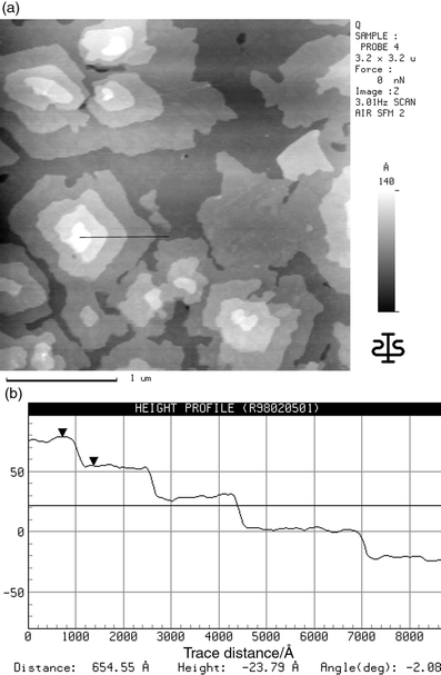 | ||
| Fig. 5 (a) SFM image of an α5T-layer on TiO2(001) with a mean thickness of 19.5 nm; (b) cross section along the line shown in (a). | ||
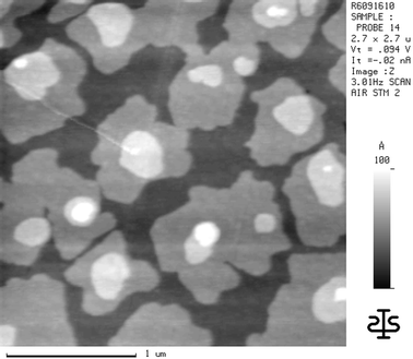
As a next step the substrate temperature upon evaporation was raised to 393 K. In the SFM image (Fig. 6) it can be seen that the island dimensions are growing further. Probably crystalline regions are detected which have an extension of several µm. The height profile in Fig. 6b demonstrates complete flatness of these regions over a large scale. The detected average roughness is below 0.01 nm. The cross sections through the probably crystalline regions again show distinct height differences of about 2.3 nm and multiples thereof. This indicates that in these regions the molecules stand with their long axis nearly perpendicular to the substrate surface. The same results are obtained for α5T films evaporated on TiO2(001) at room temperature and annealed afterwards to this temperature.
 | ||
| Fig. 6 (a) SFM image of an α5T-layer on TiO2(001) with a mean thickness of 19.5 nm; (b) cross section along the line shown in (a). | ||
In another region of this sample the flatness of the layers as observed in all experiments presented so far is disturbed, i.e. the step heights are no longer multiples of 2.3 nm. There are two possible explanations for this behavior: either the substrate temperature was so high that the molecules began to sublime or they were no longer standing with their long axis nearly perpendicular to the substrate surface.
3.2 Growth mode of α5T on conductive TiO2(001)
The TiO2(001) single crystals were reduced through annealing at temperatures above 970 K under UHV conditions. SEM measurements revealed that this process leads to an enhanced roughness of the substrate (Fig. 7a).On these substrates, films with different layer thicknesses are evaporated under systematically varied conditions as discussed in Section 3.1. For room temperature substrates the evaporation rate R was again not a critical parameter and R = 1.2 nm min−1 was chosen for all experiments described below.
Evaporation of on average 7.2 and 85 nm thick α5T films on these reduced substrates held at room temperature leads to a cluster growth of α5T films as shown in Fig. 7b,c. Here, clusters denote three-dimensional agglomerations of α5T molecules with a non-planar surface topography. The cluster dimensions are similar in height and width, as measured by SFM. This cluster growth mode results in prolonged crystallites with an average length of about 1 to 2 µm, as shown in the SFM as well as in the SEM pictures (Fig. 7b,c and 8a). These crystallites are oriented along the same direction, indicating a strong interaction with the substrate. However, no corresponding structure on the substrate (Fig. 7a) could be found.
Between the crystallites flat regions can be detected as shown in Fig. 8b. In these areas layers could be scratched off with the SFM tip indicating that these flat areas do not belong to the substrate but to α5T layers. The bad image conditions close to the very high crystallites do not allow study of the film formation in detail. However, for all measured samples, even for on average 85 nm thick α5T films, the substrate peaks (O1s and Ti2p) could be detected by XPS. Consequently, these flat layers of α5T are very low in height or are very rare.
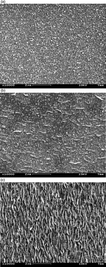 | ||
| Fig. 7 SEM-measurements of (a) the reduced (n-doped) TiO2(001) surface; (b) an α5T layer with a mean thickness of 7.2 nm; and (c) an α5T layer with a mean thickness of 85 nm on top of this surface. | ||
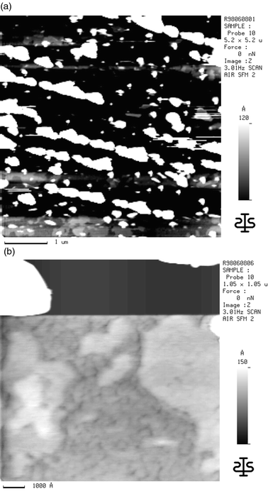 | ||
| Fig. 8 (a) SFM image of an α5T layer with a mean thickness of 10 nm on the reduced (n-doped) TiO2(001) surface; (b) higher magnification scan. | ||
Because of the cluster growth, enhancement of the substrate temperature did not lead to any improvement of the layer structure (see Section 4 below).
To avoid the negative effects of the substrate roughness caused by reduction, the substrate was polished after the reduction process and subsequently cleaned. Although the polishing procedure caused large grooves on the substrate the surface in between these scratches is smoothed (compare Fig. 7a and 9a). Evaporation of α5T on these substrates leads again to layer growth as shown in Fig. 9b,c. As on SiO surfaces8 the layers cover all surface inhomogeneities as flat patches. These patches reveal the same shape as those on flat non-conductive TiO2.
 | ||
| Fig. 9 (a) SFM image of an α5T layer with a mean thickness of 7.2 nm on the reduced (n-doped) and subsequently polished TiO2(001) surface; (b) higher magnification scan. | ||
4. Discussion
These findings can be summarized to the following film growth behavior on TiO2(001) substrates (Fig. 10). From earlier fluorescence measurements it is known that isolated α5T molecules lie flat and diffuse on smooth oxidic surfaces.9 As soon as two or more molecules meet on the surface they form aggregates. On flat substrate surfaces they align with their long axes parallel to each other and stand nearly upright on the surface. This is demonstrated by the layer heights as determined by SFM as well as by the tilt angle θ = 30° of the molecules against the surface normal as measured by fluorescence measurements.22 On topographic pinning centers, however, the molecules aggregate to three-dimensional crystalline clusters in which the molecules are no longer oriented against the surface normal. | ||
| Fig. 10 Proposed growth model of α5T on TiO2(001) (a) on a substrate with pinning centers; (b) on a substrate (area) without pinning centers. | ||
The macroscopic film quality is therefore largely influenced by the substrate flatness, the substrate temperature, and, in some cases, by the evaporation rate. On flat substrate surfaces or larger areas with a negligible amount of pinning centers the first two monolayers grow according to a Frank–Van der Merwe growth mode, i.e. layer-by-layer growth. Beginning with the third layer, a three-dimensional multilayer growth mode is observed. For room temperature substrates these layers are not crystalline. Because of the similarity of their overall appearance with layers on SiO25,7 it is assumed that they form a smectic liquid crystalline layer. Increasing the substrate temperature during evaporation gives the molecules enough energy to form films in which the islands have rectangular form and sharp edges. Annealing films originally evaporated onto room temperature substrates at elevated temperatures gives similar results. Best results are obtained at 363 K, where in thermal desorption measurements a temperature-induced disordered phase is observed in which the molecules may have an increased mobility. The so-formed islands are probably crystalline and can have dimensions in the range of several micrometers. This would be ideal for application in pn-diodes. Although LEED measurements on these layers could not be performed so far, it is not expected that these layers are oriented epitaxially with respect to the substrate surface because the growth mode is similar to that on amorphous substrates such as glass and Si wafer oxide. The growth mode is mainly determined by the molecule–molecule (van der Waals) interactions which due to the anisotropy of the molecules lead (accidentally) to a layer growth mode.
However, on surfaces with pinning centers, as they were particularly introduced by heating (and hence n-doping) of TiO2 in UHV it is more critical for the film formation to be optimized. The higher the number of pinning centers, the lower the evaporation rate and the higher the substrate temperature the higher is the probability for a given molecule to meet a pinning center and not another molecule. This then leads to cluster growth. If the deposition rate is enhanced, aggregation is kinetically favored if compared to diffusion. Therefore closed layers are formed as on flat substrates in which the molecules again stand nearly upright on the substrate surface. They cover even very rough surfaces like a carpet, as could be shown for layers on polished doped TiO2(001) which could even be formed at a medium evaporation rate. However, on unpolished n-doped TiO2(001) surfaces as well as on TiO2(011) surfaces in general, the number of pinning centers is so high that the evaporation rate for room temperature substrates could not be raised to such high values that the conditions for smooth layer formation are fulfilled.
5. Summary
The successful preparation of highly ordered α5T thin films on TiO2(001) could be demonstrated for the fully oxidized as well as for the reduced and hence n-doped crystal. The combination of scanning force microscopy and fluorescence measurements led to a detailed understanding of the growth behavior as a function of the evaporation conditions.Acknowledgements
We gratefully acknowledge technical support by W. Neu, SEM measurements by E. Nadler, H. Naarmann, BASF, Ludwigshafen, for the synthesis of the oligothiophenes, H.-J. Egelhaaf for supporting fluorescence measurements, discussions, and a critical reading of the manuscript, and mental and financial support by W. Göpel.References
- F. Garnier, R. Hajlaoui, A. Yassar and P. Srivastava, Science, 1994, 265, 1684.
- G. Horowitz, X. Z. Peng, D. Fichou and F. Garnier, J. Appl. Phys., 1990, 67, 528 CrossRef.
- H. E. Katz, A. DodabalapurZ. Bao, in Handbook of Oligo- and Polythiophenes, ed. D. Fichou, Wiley-VCH, Weinheim, 1999, p. 459. Search PubMed.
- M. Granström, M. G. HarrisonR. Friend, in Handbook of Oligo- and Polythiophenes, ed. D. Fichou, Wiley-VCH, Weinheim, 1999, p. 405. Search PubMed.
- Ch. Ziegler, in Handbook of Organic Conductive Molecules and Polymers, ed. H. Nalwa, Wiley, Chichester, 1997, p. 677 Search PubMed; D. FichouCh. Ziegler, in Handbook of Oligo- and Polythiophenes, ed. D. Fichou, Wiley-VCH, Weinheim, 1999, p. 183. Search PubMed.
- F. Martinez, R. Voelkel, D. Naegele and H. Naarmann, Mol. Cryst. Liq. Cryst., 1989, 167, 227 Search PubMed.
- O. Böhme, Ch. Ziegler and W. Göpel, Adv. Mater., 1994, 6, 587 CrossRef.
- O. Böhme, Ch. Ziegler and W. Göpel, Synth. Met., 1994, 67, 87 CrossRef.
- H.-J. Egelhaaf, P. Bäuerle, K. Rauer, V. Hoffmann and D. Oelkrug, Synth. Met., 1993, 61, 143 CrossRef CAS.
- H.-J. Egelhaaf, P. Bäuerle, K. Rauer, V. Hoffmann and D. Oelkrug, J. Mol. Struct., 1993, 293, 249 CrossRef CAS.
- H.-J. Egelhaaf and D. Oelkrug, SPIE, 1995, 2362, 398 Search PubMed.
- J. Gierschner, H.-J. Egelhaaf and D. Oelkrug, Synth. Met., 1997, 84, 529 CrossRef CAS.
- F. Van Bolhuis, H. Wynberg, E. E. Havinga, E. W. Meijer and E. G. J. Staring, Synth. Met., 1989, 30, 381 CrossRef CAS.
- W. Porzio, S. Destri, M. Maschperga and S. Brückner, Acta Polym., 1993, 44, 266 CrossRef CAS.
- W. Göpel, G. Rocker and R. Feierabend, Phys. Rev. B, 1983, 28, 3427 CrossRef CAS.
- P. J. Møller and M.-C. Wu, Surf. Sci, 1989, 224, 265 CrossRef.
- K. D. Schierbaum, S. Fischer, P. Wincott, P. Hardman, V. Dhanak, G. Jones and G. Thornton, Surf. Sci., 1997, 391, 196 CrossRef CAS.
- S. Fischer, J. A. Martin-Gago, E. Román, K. D. Schierbaum and J. L. de Segovia, J. Electron Spectrosc. Relat. Phenom., 1997, 83, 217 CrossRef CAS.
- J. Murr and Ch. Ziegler, Phys. Rev. B, 1998, 57, 7299 CrossRef CAS.
- D. Oeter, Ch. Ziegler and W. Göpel, Synth. Met., 1993, 61, 147 CrossRef CAS.
- W. Göpel, J. A. Anderson, D. Frankel, M. Jaehnig, K. Phillips, J. A. Schäfer and G. Rocker, Surf. Sci., 1984, 139, 333 CrossRef.
- H.-J. Egelhaaf, University of Tübingen, personal communication; H.-J. Egelhaaf, E. Müller, D. Oelkrug and Ch. Ziegler , in preparation. For similar measurements on glass and Si-wafer substrates, compare reference 5 and references therein. .
Footnote |
| † Basis of a presentation given at Materials Chemistry Discussion No. 2, 13–15 September 1999, University of Nottingham, UK. |
| This journal is © The Royal Society of Chemistry 2000 |