
 Open Access Article
 This Open Access Article is licensed under a Creative Commons Attribution-Non Commercial 3.0 Unported Licence
Controllable Ag nanoparticle coated ZnO nanorod arrays on an alloy substrate with enhanced field emission performance†
Mengjie Li,
Weijun Huang,
Weijin Qian *,
Boyang Liu,
Hao Lin,
Wei Li,
Li Wan and
Changkun Dong*
*,
Boyang Liu,
Hao Lin,
Wei Li,
Li Wan and
Changkun Dong*
Institute of Mirco-nano Structure & Optoelectronics, Wenzhou University, Wenzhou 325035, China. E-mail: weijinqian@wzu.edu.cn; dck@wzu.edu.cn; Fax: +86-577-86689011; Tel: +86-577-86689067
First published on 3rd October 2017
Abstract
Ag–ZnO nanocomposites were prepared on alloy substrates by two simple and inexpensive steps, i.e. synthesis of ZnO nanorod arrays (ZNAs) by a low-temperature hydrothermal method, followed by electrophoretic deposition method to coat ZNAs with Ag nanoparticles (NPs). The sizes and densities of the Ag NPs could be facilely adjusted by changing the deposition time. The field emission (FE) performances of Ag–ZnO emitters were improved greatly by adjusting the sizes and densities of the Ag NPs, and the optimized FE performance of the Ag–ZnO emitter was obtained with the lowest turn-on field of 0.86 V μm−1 and a current density up to 7.96 mA cm−2 at 4.45 V μm−1. More importantly, the Ag–ZnO emitter exhibited excellent current stabilities with 1900 min operation under only 6.5% current fluctuation. These results suggest that the Ag–ZnO composite is a promising cathode material for fabrication of future FE devices.
1 Introduction
Field emission (FE) cathodes have shown great potentials in many applications, such as flat panel displays, X-ray sources, microwave amplifier and high-brightness lighting.1 In recent years, one-dimensional (1D) nanostructures, such as carbon nanotubes (CNTs),2,3 AlN nanocones,4–6 and ZnO nanorod arrays (ZNAs) or nanowires (ZNWs),7–10 have been extensively reported for FE applications due to their high aspect ratios, good mechanical strength, and chemical stability. Especially, ZNAs or ZNWs has attracted more attentions due to advantages of controllable morphology, environment-friendship, low cost, and feasibility of large scale growth.9,10 In the past few years, great efforts have been made to improve the FE performances of ZNAs or ZNWs, such as doping,11–13 coating with other materials,14–16 or growing on the conducting substrate.17,18 Among these methods, one of the most effective strategies is to construct ZnO based composite FE materials, which can either enhance the emission sites by forming a rough surface, or improve its conductivity due to the synergistic effect between different materials.Due to good conductivity and chemical stability, Ag nanoparticles (NPs) have been widely applied to decorate various 1-D nanostructures, such as CNTs and CuO nanoribbons,19,20 and the composites exhibit good FE performances due to synergistic effects from different components. Electrophoretic deposition (EPD) is an effective technique to obtain different metal NPs with various advantages, including production uniformity, easy control of the deposition density, wide applicability, and low cost.21 So far, there are a few studies22–24 on Ag–ZnO composites and their FE performances. For example, Ye et al.22 reported two step synthesis of Ag–ZnO nanorods. Firstly, ZnO nanorods was grown on Si substrate by the solution method, then the ZnO nanorods were decorated with Ag NPs by reduction Ag salts in H2O/ethanol solution. The turn-on field of this Ag NPs-decorated ZnO nanorod emitter was 2.6 V μm−1. Warule and partners23 prepared Ag–ZnO heterostructures on Zn foil by hydrothermal method. The FE performances included the turn-on field of 1 V μm−1, the FE current density of 400 μA cm−2 at 2.24 V μm−1, and the emission current fluctuation rates of 10% in 3 h with the currents of 1 and 4 μA. The author thought that the current fluctuations probably resulted from adsorption or desorption of the residual gas atoms/molecules on the emitter surface. Yang et al.24 synthesized Ag NP decorated ZnO nanorod on glass substrates by the hydrothermal method. Before preparation of Ag–ZnO nanorods, a 50 nm-thick ZnO seed layer was deposited on a glass substrate by RF magnetron sputtering on ZnO target. The FE characteristics were obtained in the dark and under UV illumination with the turn-on fields of 3.93 and 2.04 V μm−1, respectively. The author believed that the decreasing turn-on field was mainly due to the increasing probability of tunneling through the vacuum level. In spite of achieving these advances, however, few reports have been focused on the optimization of Ag NPs and the investigations of high current density and long time operation, which is critical for practical applications of ZnO-based field emitters.
In this study, the Ag–ZnO nanocomposites were prepared on the alloy substrates by two simple and inexpensive steps, i.e. synthesis of ZNAs by a low-temperature hydrothermal method, followed by EPD to coat ZNAs with Ag NPs. The sizes and densities of Ag NPs could be facilely adjusted by changing the deposition period. As the results, the FE performances of Ag–ZnO emitters, including the turn-on field and the emission stability, were improved significantly due to the work function reduction, conductivity enhancement, and emission site increase. The results demonstrate that Ag–ZnO composite is a promising cathode material for FE devices.
2 Experimental
To prepare Ag–ZnO composites,25,26 ZNAs were prepared by a low-temperature hydrothermal method based on ZnO seed layer, followed by EPD to coat ZNAs with the Ag NPs, as shown in Fig. 1. Detailed experimental process is given as follows. | ||
| Fig. 1 Schematic illustration of the preparation of Ag–ZnO composite. | ||
Synthesis of ZnO seed films
The alloy substrates were ultrasonically cleaned by acetone, alcohol and purified water for 10–15 min, respectively. Subsequently, the alcohol solution of sodium hydroxide (NaOH, 0.03 mol L−1) was slowly dipped into the alcohol solution of the zinc acetate (Zn(NO3)2·6H2O, 0.02 mol L−1) in a three-necked flask at room temperature. The mixed solution was stirred at 60 °C for 3 h until yielding a little turbid but homogeneous solution. Then the ZnO seed solution was coated on the clean substrates by spin-coating technique. The foregoing dip-coating process was repeated several times and the coated substrates eventually experienced a heat treatment at 350 °C for 30 min to improve the adherence between the substrates and the ZnO seed films.Preparation of the ZNAs on alloy substrate
An aqueous solution of zinc nitrate (Zn(NO3)2·6H2O, 0.01 mol L−1) was dipped into the solution of hexamethylenetetramine (C6H2N4, 0.01 mol L−1). The mixed solution was stirred in a 250 mL flat-bottomed flask at room temperature to form a homogeneous solution. Then the alloy substrates coated with the ZnO seeds were immersed in the mixed solution. After the whole growth system was heated to 90 °C with 6 h, ZNAs were successfully grown on the substrate, which would later be thoroughly rinsed by distilled water to remove the residual salts, and to be dried in air at room temperature.Synthesis of the Ag–ZnO composites
Ag(NO3)2 (99.5%, Aladdin) were dispersed in ethanol and sonicated for about 1 hour to form a homogeneous solution. The alloy substrate (working electrode) and the stainless steel (counter electrode) were separated with the distance of 1 cm and they were immersed into the Ag(NO3)2 solution (1 × 10⁻³ mol L−1) by the EPD method with the constant potential of 100 V. After the EPD process, the products were conducted the annealing process in the furnace at 400 °C for 60 min under the protection of Ar, then the Ag–ZnO nanocomposites could be obtained. The as-obtained samples are denominated as Ag–ZnO-x, where x is the deposition time.Characterization and FE measurement
The morphologies and microstructures of the products were observed by scanning electron microscopy (SEM; JEOL JSM-7100F) and high resolution transmission electron microscopy (HRTEM; JEM-2100). The components of the as-prepared products were characterized by X-ray diffraction (XRD; GmbH SMART APEX), and the composition analysis were performed by energy-dispersive X-ray analysis (EDS) and X-ray photoelectron spectroscopy (XPS; PHI 5000 VersaProbe). Field emission performances were investigated with a two parallel plate structure in a vacuum chamber under the pressure of about ∼10−6 Pa and all the test samples were 0.16 cm2 in area. The as-obtained samples were used as cathode and the silicon substrates were used as anode. The two electrodes were separated with the distance of 500 μm. The FE characteristics were measured by a Keithley 2440 multimeter and a Keithley 248 high voltage supply.3 Results and discussion
Typical morphologies of the products are shown in Fig. 2. ZnO nanorod arrays were grown on the alloy substrate with the diameters of 80−120 nm (Fig. 2a, see the SI-1 in ESI†). After EPD, the surfaces of ZNAs were coated with Ag NPs of different sizes and densities depending on the EPD periods (Fig. 2b–d). With 5 min deposition, the Ag NPs had the sizes of 10–20 nm (Fig. 2b). As the deposition time is prolonged to 10 min, the density of the Ag NPs increases obviously with the sizes in 10–40 nm range (Fig. 2c). The longer the deposition time is, the larger sizes and higher densities the Ag NPs are (Fig. 2d–f).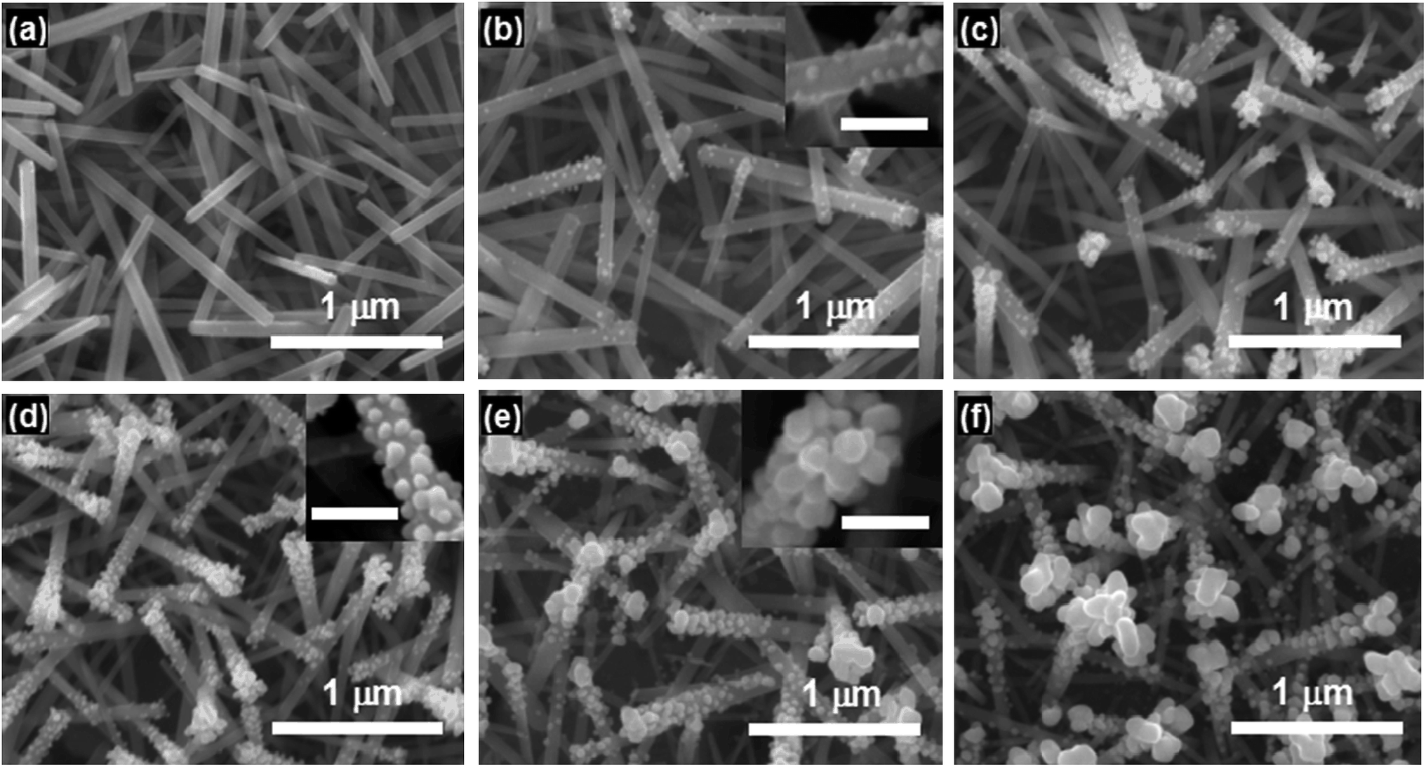 | ||
| Fig. 2 SEM images of (a) pristine ZnO nanorod arrays and (b–f) the products obtained by 5, 10, 20, 30 and 40 min deposition, respectively. Scale bars in the insets correspond to 200 nm. | ||
Typical TEM images of the Ag–ZnO-20 composite are shown in Fig. 3 (see the SI-2 in ESI†). The stem diameters of ZnO nanorods are in 80–120 nm range and the diameters of Ag NPs are 5–25 nm. The ZnO nanorods have the hexagonal wurtzite structure growing along [0001] direction (Fig. 3b), in agreement with the XRD result (see the SI-3 in ESI†). HRTEM image for Ag–ZnO sample suggests that the Ag NPs are attached on the surface of the ZnO nanorods, with a lattice spacing of about 0.238 nm corresponding to d111 value of Ag (Fig. 3c), in agreement with the XRD characterization (also see the SI-3 in ESI†). The components of the Ag–ZnO product could be confirmed by the EDS analysis (Fig. 3d), which exhibited the signals of Zn, O, and Ag, as expected (see the SI-4 in ESI†).
 | ||
| Fig. 3 Typical TEM images of the Ag–ZnO-20 composite (a) Low resolution TEM image of the Ag–ZnO sample, and HRTEM images of (b) ZnO nanorods and (c) Ag nanoparticle, (d) EDS analysis of the sample in (a). | ||
Further characterization by XPS was employed to detect the composition of the Ag–ZnO sample. As shown in Fig. 4a (also see the SI-5 in ESI†), the survey spectrum exhibited the signals of Zn, O, and Ag, whereas the C peak was from the sample holder in the XPS chamber (see the SI-6 in ESI†). As shown in Fig. 4b, two peaks from Zn–O bonds were detected at 1021.6 and 1044.9 eV, corresponding to the Zn 2p3/2 and Zn 2p1/2, respectively.27 For the O1s spectrum (Fig. 4c), it can be deconvolved into three peaks by Gaussian fitting. The peak from O–Zn bonds was observed at 530.4 eV,27,28 another two peaks at 531.5 and 532.4 eV could be attributed to the oxygen defect and the chemisorbed oxygen, respectively (see the SI-7 in ESI†).28,29 As shown in Fig. 4d, two peaks at 367.6 eV and 373.3 eV should be assigned to Ag 3d5/2 and Ag 3d3/2, respectively. Compared with the binding energies (BE) of metallic Ag0 (368.2 eV) and Ag+ (367.2 eV),30 the BE value of Ag 3d5/2 in the Ag–ZnO sample shifts obviously to the lower BE, due to the interaction between the Ag NPs and the ZNAs, implying the existence of the charge transfer from the Ag NPs to the ZNAs.30
 | ||
| Fig. 4 XPS spectra of the Ag–ZnO sample, (a) survey; (b) Zn 2p; (c) O 1s; (d) Ag 3d. Note: the peak for C 1s at 284.6 eV is used for calibration. | ||
Structural and compositional analysis shows clearly that Ag NPs are successfully coated on the ZNAs and the charge transfer exists from the Ag NPs to ZNAs. The FE properties are investigated for the pristine ZNAs and the Ag–ZnO composite emitters. The turn on fields Eto and threshold fields Ethr (the electric field to generate an emission current density of 10 μA cm−2 and 1.0 mA cm−2, respectively) of different samples are listed in Table 1. Fig. 5a depicts the J–E (current density versus applied field) curves of these samples with the cathode–anode distance of 500 μm. Compared with the pristine ZnO nanorods, all the Ag–ZnO composite samples exhibited smaller Eto and Ethr values, which could be attributed to several factors. Firstly, the work function (ϕ) of the Ag–ZnO composite (ϕAg–ZnO ∼ 4.7 eV, see the SI-8 in ESI†) is lower than that of the pristine ZnO nanorods due to the decoration of the low work function Ag NPs (ϕZnO ∼ 5.3 eV, ϕAg ∼ 4.3 eV),22–24 similar to the case of Ag-decorated CuO nanoribbons.20 Secondly, the decoration of Ag NPs on ZNAs could enhance the conductivity of the ZnO nanorods due to more electrons injection from the Ag NPs, as confirmed by XPS characterization, which benefits the electron emission for these hybrid nanostructures. Thirdly, the Ag NPs on the ZNAs serve as emission sites, leading to the emission field reduction and high current enhancement, similar case could be found in CsI-decorated AlN nanocones.5
| Sample | Turn-on field (V μm−1) | Threshold field (V μm−1) |
|---|---|---|
| ZnO | 4.66 | — |
| Ag–ZnO-5 | 3.19 | 10.16 |
| Ag–ZnO-10 | 1.96 | 6.40 |
| Ag–ZnO-20 | 0.86 | 2.85 |
| Ag–ZnO-30 | 1.36 | 3.74 |
| Ag–ZnO-40 | 1.59 | 5.29 |
 | ||
| Fig. 5 J–E curves (a) and F–N plots (b) of the products; (c) and (d) emission stability test of the ZnO nanorods and Ag–ZnO-20 composite, respectively. | ||
FE properties of the Ag–ZnO composite samples depend highly on the size and density of the Ag nanoparticles, as shown in Fig. 5a (Table 1). For Ag–ZnO-5, the density of Ag NPs is relatively low, so its FE properties are only slightly better than those of the pristine one. The Ag–ZnO-20 composite has the best FE performance among all these samples due to adequate amount of Ag NPs attached on the surface of the ZNAs. With further increasing the EPD period, both the size and density of the Ag NPs increase accordingly, leading to the drop of the aspect ratio and the increase of the screening effect. When the deposition time reached 40 min, the top of the ZNA was totally covered by the Ag NPs (Fig. 1f), which hindered the electron emission from ZNAs. Thus the FE performance decays with the deposition period of over 20 min. Similar cases were observed for the CsI-coated AlN nanocones and ZnO-decorated carbon nanotubes.5,31 In comparison with the some semiconductor nanomaterials, such as AlN nanocones and ZnO-based nanostructures, the Ag–ZnO-20 emitter shows better FE performances (see Table 2), e.g. the lower turn-on field of 0.86 V μm−1 and the current density up to 7.96 mA cm−2 with the applied field of 4.45 V μm−1, better than previous reports of the AlN nanocones and ZnO-based field emitters. In addition, further effort should be focused on improving the emission current of ZnO-based field emitters by doping11,12 to match with the FE performances of CNTs.
| Nanostructures | Turn-on field (V μm−1) | Maximum current density (mA cm−2) | Stability test (min) | Ref. |
|---|---|---|---|---|
| CNTs | 1.50 | 100 mA cm−2 | Not stated | 2 |
| Doped AlN nanocones | 7.07 | Not stated | 120 min, ±4% | 6 |
| ZnO nanorods | 2.1 | 470 μA cm−2 at 3 V μm−1 | Not stated | 9 |
| Pt–ZnO nanorods | 1.3 | Not stated | Not stated | 22 |
| Ag–ZnO nanorods | 2.6 | Not stated | Not stated | 22 |
| Au–ZnO nanopillars | 2.65 | 2.11 mA cm−2 at 5 V μm−1 | 60 min, 6 ± 2% | 33 |
| ZnO–CNT heterostructure | 2.1 | 7 mA cm−2 at 4.95 V μm−1 | Not stated | 14 |
| Ag–ZnO heterostructure | 1 | 400 μA cm−2 at 2.24 V μm−1 | 180 min, 10% | 23 |
| Ag–ZnO nanorods | 2.04 | Not stated | Not stated | 24 |
| ZnO nanorods | 4.66 | 0.65 mA cm−2 at 14.65 V μm−1 | 445 min, 15% | This paper |
| Ag–ZnO-20 composite | 0.86 | 7.96 mA cm−2 at 4.45 V μm−1 | 1900 min, 6.5% | This paper |
As shown in Fig. 5b, a two-section slope characteristic is demonstrated in the FN curves for all samples. These multistage slope characteristics are also observed in other field emitters, which might be attributed to the space charge effect, localized state and adsorbates.14,32–38 Generally, the field enhancement factor exhibits a small value at a low applied field and a large value at a high applied field. However, in this work, FE phenomenon of the slope feature is just opposite, probably due to the surface states or shallow levels resulted from the intrinsic defects of the ZNAs.35,36,38 Because different defects in the ZnO nanorods, such as Zn interstitials or oxygen vacancies, are formed during the hydrothermal reaction, due to the high Zn concentration and low oxygen concentration in the reaction solution,38 in agreement with the XPS result. In addition, some adsorbents are attached on the surface of the samples, which may change the work function of the samples under different applied field. The gas adsorption will easily happen at low applied field, which can reduce the work function of the samples and the gas desorption will arise at high applied field, leading to two stage deviations of F–N curves in all samples.36
Another possible reason for the two-section slope characteristics is based on the fact that electron emit from the conduction band (CB) and valence band (VB).39,40 Generally, the electrons from the CB dominate the low field emission, while increasing further the applied field, the electrons from VB will also play the key role in the FE process. According to the F–N equation: β = −6.83 × 10³ × ϕ3/2/slope,41 where β is the enhancement factor, ϕ is the work function, assuming β is constant, the slope (S) of the ln(J/E2) versus 1/E plot is proportional to ϕ3/2. Therefore, the change in the slope can be obtained by SH/SL = (ϕH/ϕL)3/2, where H and L refer to the high and low applied fields, respectively. Assuming the emission electrons are from the CB (ϕZnO = 5.3 eV, ϕAg–ZnO = 4.7 eV, see SI-8 in ESI†),40 if the electrons from the VB (∼3.37 eV below the CB) participate in the FE process, the effective work functions (ϕE) of ZnO nanorods and Ag–ZnO composite are estimated with the values of 8.67 and 8.07 eV, respectively.40 Thus, the ratio of two-section slope (SH/SL) correspond to 2.09 and 2.25, respectively. For the pristine ZnO nanorods, by linear fitting, the ratio of the two-section slope is 2.86. For the Ag–ZnO composites, with the increasing deposition time from 5 to 30 min, the ratios of the two-section slope are 3.18, 3.42, 4.37 and 6.85, respectively, higher than the calculated values. Interestingly, with the deposition time up to 40 min, the ratio of the two-section slope become small (2.22), probably due to the weakness of the intrinsic field emission from ZNAs caused by the redundant Ag NPs on the top of the ZnO nanorods (see Fig. 2f).
The emission stability testing of the pristine ZnO nanorods and the Ag–ZnO-20 sample are shown in Fig. 5c and d. As for the pristine ZnO nanorods (Fig. 5c), the current decays gradually after ca. 200 min stable emission and the current fluctuation is found to be ∼15% during the whole emission period of 445 min, probably due to the changed morphologies resulted from the Joule heat or ion bombardment in the FE process.42 In comparison with the pristine ZNAs, the current of the Ag–ZnO-20 sample (Fig. 5d) do not show obvious decay and the current fluctuation is observed with only about 6.5% at 689 μA cm−2 after 1900 min emission, probably attributed to the enhanced thermal conductivity from the Ag NPs,43,44 and the good adhesion between ZNAs and Ag NPs. The results suggest that Ag–ZnO composite may be a promising cathode material for fabrication of future ZnO-based FE devices.
To elaborate the enhancement of FE performances for the Ag–ZnO composite, the energy band diagrams of pristine ZnO nanorods and Ag–ZnO composite in FE process are shown in Fig. 6. As shown in Fig. 6a, when the pristine ZnO nanorods is operated under the external electric field, an energy well is formed at the depleted region due to the energy band bending, then the accumulation of electrons will appear in this region. In comparison with the pristine ZnO nanorods, when the Ag NPs are attached to the surface of ZNAs, the energy band bending at the interface and the Fermi level of ZnO are both changed. Meanwhile, an enhanced energy well is formed at the interfaces of ZnO and Ag (Fig. 1b). Since the work function of Ag is lower than that of ZnO (ϕZnO ∼ 5.3 eV, ϕAg ∼ 4.3 eV),22–24 more electrons will move from the Ag NPs to ZnO nanorods, which can enhance the conductivity of the ZnO nanorods. Thus, for the Ag–ZnO composites, large quantities of the excited electrons will be gathered and trapped at the depleted region (Fig. 1b), which can increase the probability of tunneling through the vacuum level under the external electric field.24
 | ||
| Fig. 6 The energy band diagrams of (a) the pristine ZnO nanorods and (b) the Ag–ZnO composite in field emission process. Note: CB and VB is the conduction and valence band, respectively. Ef is Fermi level and ϕ is work function. | ||
4 Conclusions
In summary, the Ag–ZnO nanocomposites were successfully grown on the alloy substrate via two simple and inexpensive steps, i.e. synthesis of ZnO nanorod arrays by a low-temperature hydrothermal method, followed by EPD method to coat ZNAs with the Ag NPs. The sizes and densities of the Ag NPs could be facilely adjusted by changing the EPD period, leading to the optimization of the Ag–ZnO field emitters. The Ag–ZnO emitters presented excellent field emission performance with the lowest turn-on field of 0.86 V μm−1 and the current density up to 7.96 mA cm−2 at 4.45 V μm−1. The emitter showed improvement on stability with only 6.5% fluctuation at 689 μA cm−2 after 1900 min operation. This work suggests that the Ag–ZnO emitter is very promising for applications in different types of FE devices.Conflicts of interest
There are no conflicts to declare.Acknowledgements
This work was financially supported by National Science Foundation of China (No. 51302193, 61620106006, 11274244).Notes and references
- N. S. Xu and S. E. Huq, Mater. Sci. Eng., R, 2005, 48, 47–189 CrossRef.
- S. Sridhar, L. Ge, C. S. Tiwary, A. C. Hart, S. Ozden, K. Kalaga, S. Lei, S. V. Sridhar, R. K. Sinha, H. Harsh, K. Kordas, P. M. Ajayan and R. Vajtai, ACS Appl. Mater. Interfaces, 2014, 6, 1986–1991 CAS.
- D. H. Shin, K. N. Yun, S.-G. Jeon, J. Kim, Y. Saito, W. I. Milne and C. J. Lee, Carbon, 2015, 89, 404–410 CrossRef CAS.
- N. Liu, Q. Wu, C. Y. He, H. S. Tao, X. Z. Wang, W. Lei and Z. Hu, ACS Appl. Mater. Interfaces, 2009, 1, 1927–1930 CAS.
- W. J. Qian, H. W. Lai, X. Z. Pei, J. Jiang, Q. Wu, Y. L. Zhang, X. Z. Wang and Z. Hu, J. Mater. Chem., 2012, 22, 18578–18582 RSC.
- Q. Wu, N. Liu, Y. L. Zhang, W. J. Qian, X. Z. Wang and Z. Hu, J. Mater. Chem. C, 2015, 3, 1113–1117 RSC.
- K. Mahmood, S. B. Park and H. J. Sung, J. Mater. Chem. C, 2013, 1, 3138–3149 RSC.
- C. X. Wu, F. S. Li, Y. G. Zhang and T. L. Guo, Carbon, 2012, 50, 3622–3626 CrossRef CAS.
- R. J. Zou, G. J. He, K. B. Xu, Q. Liu, Z. Y. Zhang and J. Q. Hu, J. Mater. Chem. A, 2013, 1, 8445–8452 CAS.
- Z. Y. Zhang, Y. Y. Lv, J. F. Yan, D. D. Hui, J. N. Yun, C. X. Zhai and W. Zhao, J. Alloys Compd., 2015, 650, 374–380 CrossRef CAS.
- F. J. Sheini, M. A. More, S. R. Jadkar, K. R. Patil, V. K. Pillai and D. S. Joag, J. Phys. Chem. C, 2010, 114, 3843–3849 CAS.
- D. L. Shao, J. Gao, G. Q. Xin, Y. P. Wang, L. Li, J. Shi, J. Lian, N. Koratkar and S. Sawyer, Small, 2015, 11, 4785–4792 CrossRef CAS PubMed.
- A. K. Rana, P. Bankar, Y. Kumar, M. A. More, D. J. Late and P. M. Shirage, RSC Adv., 2016, 6, 104318–104324 RSC.
- N. S. Liu, G. J. Fang, W. Zeng, H. Long and X. Z. Zhao, J. Phys. Chem. C, 2011, 115, 14377–14385 CAS.
- G. J. Wang, M. Y. Li, C. H. Chen, S. S. Lv, J. C. Liao and Z. C. Li, Dalton Trans., 2016, 45, 8777–8782 RSC.
- J. C. Lin, B. R. Huang and T. C. Lin, Appl. Surf. Sci., 2014, 289, 384–387 CrossRef CAS.
- J. P. Liu, X. T. Huang, Y. Y. Li, X. X. Ji, Z. K. Li, X. He and F. L. Sun, J. Phys. Chem. C, 2007, 111, 4990–4997 CAS.
- Y. Huang and G. L. Yuan, Mater. Lett., 2012, 82, 85–87 CrossRef CAS.
- L. F. Chen, L. Wang, X. G. Yu, S. J. Zhang, D. Li, C. Xu, L. S. Zeng, S. Zhou, J. J. Zhao, F. Guo, L. Q. Hu and D. Yang, Appl. Surf. Sci., 2013, 265, 187–191 CrossRef CAS.
- S. M. Wu, F. Li, L. G. Zhang and Z. Li, Mater. Lett., 2016, 171, 220–223 CrossRef CAS.
- L. Besra and M. L. Liu, Prog. Mater. Sci., 2007, 52, 1–61 CrossRef CAS.
- C. H. Ye, Y. Bando, X. S. Fang, G. Z. Shen and D. Golberg, J. Phys. Chem. C, 2007, 111, 12673–12676 CAS.
- S. S. Warule, N. S. Chaudhari, R. T. Khare, J. D. Ambekar, B. B. Kale and M. A. More, CrystEngComm, 2013, 15, 7475–7483 RSC.
- C. C. Yang, Y. K. Su, M. Y. Chuang, H. C. Yu and C. H. Hsiao, IEEE Trans. Electron Devices, 2015, 62, 2300–2305 CrossRef CAS.
- X. T. Yin, W. X. Que and F. Y. Shen, J. Sol-Gel Sci. Technol., 2012, 63, 279–285 CrossRef CAS.
- X. T. Yin, W. X. Que and F. Y. Shen, Thin Solid Films, 2011, 520, 186–192 CrossRef CAS.
- R. H. Zha, R. Nadimicherla and X. Guo, J. Mater. Chem. A, 2015, 3, 6565–6574 CAS.
- L. W. Lai and C. T. Lee, Mater. Chem. Phys., 2008, 110, 393–396 CrossRef CAS.
- S. Jeong, Y. G. Ha, J. Moon, A. Facchetti and T. J. Marks, Adv. Mater., 2010, 22, 1346–1350 CrossRef CAS PubMed.
- W. W. Lu, S. Y. Gao and J. J. Wang, J. Phys. Chem. C, 2008, 112, 16792–16800 CAS.
- Y. M. Ho, W. T. Zheng, Y. A. Li, J. W. Liu and J. L. Qi, J. Phys. Chem. C, 2008, 112, 17702–17708 CAS.
- A. Ghosh, P. Guha, R. Thapa, S. Selvaraj, M. Kumar, B. Rakshit, T. Dash, R. Bar, S. K. Ray and P. V. Satyam, Nanotechnology, 2016, 27, 125701 CrossRef PubMed.
- P. Y. Chen, T. C. Cheng, J. H. Tsai and Y. L. Shao, Nanotechnology, 2009, 20, 1–9 Search PubMed.
- W. J. Qian, Y. L. Zhang, Q. Wu, C. Y. He, Y. Zhao, X. Z. Wang and Z. Hu, J. Phys. Chem. C, 2011, 115, 11461–11465 CAS.
- N. S. Ramgir, D. J. Late, A. B. Bhise, I. S. Mulla, M. A. More, D. S. Joag and V. K. Pillai, Nanotechnology, 2006, 17, 2730–2735 CrossRef CAS.
- C. X. Xu, X. W. Sun, S. N. Fang, X. H. Yang, M. B. Yu, G. P. Zhu and Y. P. Cui, Appl. Phys. Lett., 2006, 88, 161921 CrossRef.
- C. K. Dong and M. C. Gupta, Appl. Phys. Lett., 2003, 83, 159–161 CrossRef CAS.
- J. P. Liu, C. X. Xu, G. P. Zhu, X. Li, Y. P. Cui, Y. Yang and X. W. Sun, J. Phys. D: Appl. Phys., 2007, 40, 1906–1909 CrossRef CAS.
- A. A. Al-Tabbakh, M. A. More, D. S. Joag, I. S. Mulla and V. K. Pillai, ACS Nano, 2010, 4, 5585–5590 CrossRef CAS PubMed.
- T. Premkumar, Y. S. Zhou, Y. F. Lu and K. Baskar, ACS Appl. Mater. Interfaces, 2010, 10, 2863–2869 Search PubMed.
- V. S. Kale, R. R. Prabhakar, S. S. Pramana, M. Rao, C. H. Sow, K. B. Jinesh and S. G. Mhaisalkar, Phys. Chem. Chem. Phys., 2012, 14, 4614–4619 RSC.
- X. D. Wang, J. Zhou, C. S. Lao, J. H. Song, N. S. Xu and Z. L. Wang, Adv. Mater., 2007, 19, 1627–1631 CrossRef CAS.
- D. I. Florescu, L. G. Mourokh, F. H. Pollak, D. C. Look, G. Cantwell and X. Li, J. Appl. Phys., 2002, 91, 890–892 CrossRef CAS.
- F. Xin and L. Li, Composites, Part A, 2011, 42, 961–967 CrossRef.
Footnote |
| † Electronic supplementary information (ESI) available. See DOI: 10.1039/c7ra09985a |
| This journal is © The Royal Society of Chemistry 2017 |