 Open Access Article
 This Open Access Article is licensed under a
 Creative Commons Attribution 3.0 Unported Licence
Chemical and electronic structure of the heavily intermixed (Cd,Zn)S:Ga/CuSbS2 interface†
C.
Hartmann
 a,
R. E.
Brandt
b,
L. L.
Baranowski
cd,
L.
Köhler
a,
E.
Handick
a,
R.
Félix
a,
R. G.
Wilks
ae,
A.
Zakutayev
c,
T.
Buonassisi
b and
M.
Bär
*aefg
a,
R. E.
Brandt
b,
L. L.
Baranowski
cd,
L.
Köhler
a,
E.
Handick
a,
R.
Félix
a,
R. G.
Wilks
ae,
A.
Zakutayev
c,
T.
Buonassisi
b and
M.
Bär
*aefg
aHelmholtz-Zentrum Berlin für Materialien und Energie GmbH (HZB), Berlin, Germany. E-mail: marcus.baer@helmholtz-berlin.de
bMassachusetts Institute of Technology (MIT), Cambridge, Massachusetts, USA
cNational Renewable Energy Laboratory, Golden, Colorado 80401, USA
dPhysics Department, Colorado School of Mines, Golden, Colorado 80401, USA
eEnergy Materials In-Situ Laboratory Berlin (EMIL), HZB, Berlin, Germany
fHelmholtz-Institute Erlangen-Nürnberg for Renewable Energy (HI ERN), Berlin, Germany
gFriedrich-Alexander-Universität Erlangen-Nürnberg, Erlangen, Germany
First published on 11th May 2022
Abstract
The interface formation and chemical and electronic structure of the (Cd,Zn)S:Ga/CuSbS2 thin-film solar cell heterojunction were studied using hard X-ray photoelectron spectroscopy (HAXPES) of the bare absorber and a buffer/absorber sample set for which the buffer thickness was varied between 1 and 50 nm. We find a heavily intermixed interface, involving Cu, Zn, and Cd as well as significant Ga and Cu profiles in the buffer. The valence band (VB) offset at the buffer/absorber interface was derived as (−1.3 ± 0.1) eV, which must be considered an upper bound as the Cu diffused into the buffer might form a Cu-derived VB maximum located closer to the Fermi level. The estimated conduction band minimum was ‘cliff’-like; a situation made more severe considering the Cu-deficiency found for the CuSbS2 surface. The complex interface structure’s effect on the performance of (Cd,Zn)S:Ga/CuSbS2-based solar cells and its limitation is discussed together with possible mitigation strategies.
Introduction
CuSbS2 is a promising photovoltaic absorber based on earth-abundant elements with good optical properties, i.e., a direct band gap of 1.5–1.6 eV and large absorption coefficient.1 However, using device heterostructures similar to kesterite- and chalcopyrite-based solar cells, the power conversion efficiency of CuSbS2-based solar cells has so far only exceeded 3%.2,3 Density of states (DOS) calculations and valence band measurements suggest that the performance of these cells may be limited by a non-ideal energy level alignment at the buffer/absorber (i.e., CdS/CuSbS2) interface.4 The (for a buffer material) relatively small band gap of the CdS layer causes losses due to absorption in the ultraviolet region of the solar spectrum (having a negative impact on the achievable short circuit current) and purportedly leads to a large negative conduction band offset (CBO) between buffer layer and absorber, increasing the probability of recombination losses at the interface (limiting the open circuit voltage, VOC). Alloying CdS with ZnS increases the band gap of the buffer – but also increases its resistivity – as a function of Zn content; Ga doping is suggested as a mitigation strategy. Ga-doped (Cd,Zn)S (“(Cd,Zn)S:Ga”) is thus proposed as a promising alternative to CdS, providing sufficient electrical conductivity and a more beneficial energy level alignment.5 However, the performance of resulting solar cells shows only a small VOC improvement. To clarify this seeming discrepancy, we studied a (Cd,Zn)S:Ga/CuSbS2 sample set with varying thickness of the (Cd,Zn)S:Ga buffer layer by hard X-ray photoelectron spectroscopy (HAXPES) to gain detailed insight into the interface formation and resulting chemical and electronic structure.Experimental section
The CuSbS2 thin-film solar cell absorbers have been prepared by RF magnetron sputtering on Mo/glass substrates at 400 °C including a subsequent annealing step in an Sb2S3 atmosphere according to ref. 5–7. The (Cd,Zn)S:Ga buffers were prepared by atomic layer deposition (ALD) at a growth temperature of 150 °C (for more details see ref. 5). Prior to buffer deposition, the CuSbS2 absorbers were etched in an aqueous 0.1 mol l−1 KOH solution for 30 min to remove the formed Sb-rich surface oxide. To vary the thickness of the (Cd,Zn)S:Ga buffer layer, the number of ALD cycles was varied, resulting in (nominal) buffer thicknesses of 1, 4, 10, and 50 nm.After preparation at NREL, the samples were transported to the HZB in sealed vacuum bags to minimize air exposure. Samples were unpacked and mounted on suitable holders in an inert N2-purged glovebox. Synchrotron-based hard X-ray photoelectron spectroscopy (HAXPES) measurements with an excitation energy of 2003 eV (from here on referred to as 2 keV) were carried out at the HiKE endstation8 located at HZB’s BESSY II KMC-1 beamline.9 This station is equipped with a Scienta R4000 hemispherical electron energy analyzer. The base pressure of the endstation was <5 × 10⁻⁹ mbar. For the HAXPES measurements significant efforts were made to avoid air exposure of the mounted samples by transferring them from the glove box in which they were mounted into the HiKE endstation loadlock via N2-filled glovebag. The energy scale for all measurements was calibrated by measuring Au 4f spectra of a clean, electrically grounded Au foil and setting the Au 4f7/2 binding energy (BE) to 84.00 eV.10 For all samples, HAXPES survey spectra and detail spectra of the most prominent core levels (Ga 2p, Zn 2p, Sb 3d, O 1s, Cd 3d, C 1s, S 2p) and the valence band maximum (VBM) region were collected using a pass energy of 200 eV, resulting in a total energy resolution of ≈0.25 eV. The CuSbS2 absorber has been characterized before and after the KOH-etch step (to generate the same sample surface properties present prior to buffer deposition). The resulting changes in the chemical surface structure of the CuSbS2 absorbers are best visualized by the comparison of the resulting survey and Sb 3d detail spectra shown in the ESI, Fig. S1 and S2.† To derive the detailed picture of the chemical and electronic interface structure, only the data of the KOH-etched CuSbS2 absorber (referred to in the manuscript as “bare CuSbS2”) is used.
For some samples, indications of sample charging during the HAXPES analysis were observed. In most cases, this issue could be mitigated by optimizing the sample position (i.e., minimizing the distance between measurement spot and electric contact of the sample). This mitigation strategy was less effective as (Cd,Zn)S:Ga buffer layer thickness increased. For the 10 and 50 nm thick (Cd,Zn)S:Ga buffer layer samples, no HAXPES measurement was possible without clearly apparent charging, leading to a reproducible shift of the C 1s line for these samples of up to ≈0.7 eV towards higher binding energies (BE, see Fig. S3†). This is in-line with the expected high resistivity of the (Cd,Zn)S films;5 a situation that is, for the purposes of HAXPES measurements, not sufficiently improved by Ga doping. However, this charging did not appear to affect the spectral shape of the recorded photoemission lines allowing their quantification.
Simultaneous curve fit analysis of respective sets of HAXPES detail spectra were conducted with the Unifit 2016 software11 using Voigt function profiles, keeping the Lorentzian and Gaussian full width at half maximum (FWHM) values fixed for the same spectral components. The HAXPES core level spin–orbit doublets were fitted with two Voigt profiles with intensity ratios set to obey the 2j + 1 multiplicity rule. Sb 3d3/2 was fitted instead of the Sb 3d5/2 (which overlaps with O 1s) using a linear background. Cu 2p3/2, Zn 2p3/2 and Cd 3d5/2 have been fitted with a maximum of two species, with a fixed chemical shift between the two species and a Shirley background. Ga 2p3/2 was fitted with one species and a Shirley background. To derive composition ratios, the corresponding line intensities were corrected by their respective photoionization cross sections,12,13 inelastic mean free path14 and transmission function of the analyzer (see Table S1†).
Results and discussion
The HAXPES survey spectra of the sample thickness series are shown in Fig. 1. All expected photoemission lines and Auger features are present: the absorber-related Cu 2p and Sb 3d lines have the highest intensity in the bare absorber spectrum (black spectrum in Fig. 1) and, with increasing buffer layer thickness, the intensity of the Cu 2p and Sb 3d lines decreases. In parallel, the buffer-related photoemission lines, e.g., Ga 2p, Zn 2p, and Cd 3d, intensity increases. No systematic intensity evolution of the S-related lines (here prominently the S 2p and S 2s lines) is observed as S is present in both the absorber and buffer layers. Significant oxygen and carbon related photoemission (O 1s and C 1s) lines can be identified, possibly reflecting incorporation of oxygen and/or carbon in the studied samples during preparation (the organic compounds used as ALD precursors could act as carbon source and oxygen (or water) could be present as residual gas in the sputter and ALD systems or could be introduced during the wet-chemical KOH etch step) or a surface contamination layer formed as a result of insufficient means of limiting exposure to ambient conditions – despite the efforts described above.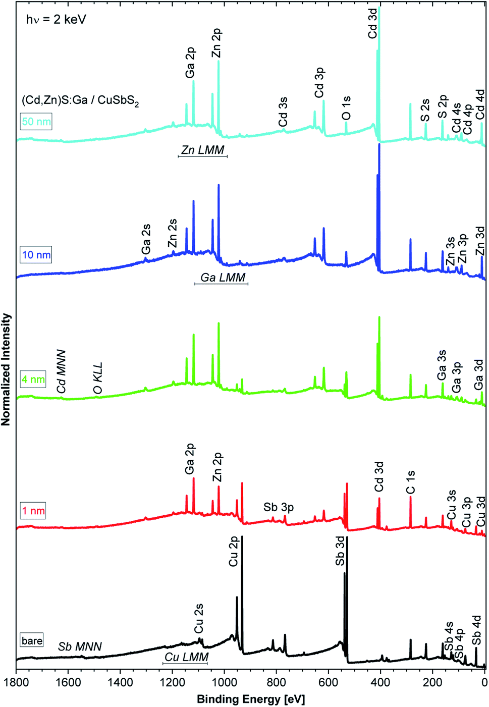 | ||
| Fig. 1 HAXPES survey spectra recorded with 2 keV of the bare CuSbS2 absorber (bottommost spectrum) and of the (Cd,Zn)S:Ga/CuSbS2 samples with buffer thicknesses varying from 1 nm (spectrum second from the bottom) to 50 nm (topmost spectrum). Vertical offsets were added for clarity. | ||
Fig. 2 shows the Sb 3d3/2 spectra for the studied samples with corresponding fits. The fits describe the data reasonably well when at least two components are assumed. The main contribution (component 1: blue peak) can be ascribed to Sb in CuSbS2 (ref. 4) while the second minor contribution (component 2: green peak) can be ascribed to SbOx.15 Different bond angles and distances in this compound of presumably less order might be an explanation for the significantly broadened peak shape. Note that for the bare CuSbS2 absorber sample, KOH etching minimizes this contribution compared to the non-etched (oxidized) sample (see Fig. S2†) but is not able to remove it completely. Upon (Cd,Zn)S:Ga buffer deposition, and with increasing buffer layer thickness, we observe a decrease in Sb 3d3/2 intensity (note the increasing magnification factors in Fig. 2) as expected but also an increasing (relative) SbOx contribution, suggesting that the SbOx layer is located in the proximity of the CuSbS2 absorber surface. Also the BE of the main Sb 3d3/2 contribution shifts by approximately +0.2 eV for the 4 nm (Cd,Zn)S:Ga/CuSbS2 sample (i.e., a sample that is considered to be not affected by charging, see Fig. S3† and related discussion) with respect to the bare absorber (for which the BE position is indicated as blue vertical line in the panels of Fig. 2). For the thickest buffer layer (50 nm) no Sb signal is detected, indicating that the buffer layer covers the absorber completely with a minimum thickness exceeding the HAXPES information depth (see ESI† for more details).
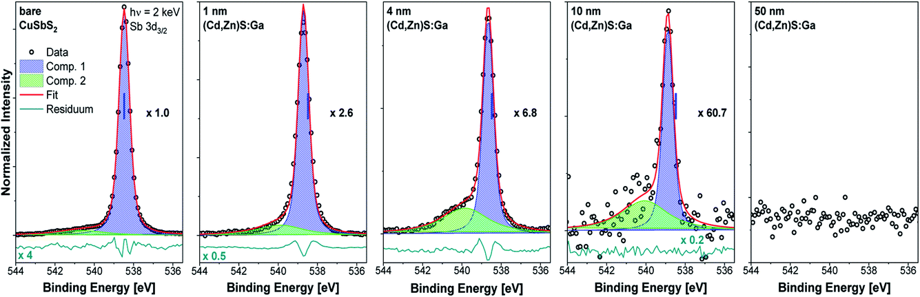 | ||
| Fig. 2 Sb 3d3/2 HAXPES detail spectra recorded with 2 keV of the bare CuSbS2 absorber (leftmost panel) and of the (Cd,Zn)S:Ga/CuSbS2 samples with buffer thicknesses varying from 1 nm (panel second from left) to 50 nm (rightmost panel). Spectra have been normalized to the background at low BE. The background-subtracted data is shown together with the fits and resulting residuals (i.e., [data − fit] – shown on different scale if required with scaling factor indicated as e.g., ×0.5). Additionally, the magnification factors are stated (as e.g., ×1.0) that were applied to show all spectra on the same intensity scale as that of the bare absorber. The vertical blue line indicates the BE position of the peak location in the spectrum of the absorber. | ||
Fig. 3 shows the Cu 2p3/2 fits for the bare CuSbS2 absorber and different (Cd,Zn)S:Ga buffer layer thicknesses. The fit of the bare absorber shows only one Cu species (component 1: blue peak) assigned to Cu in CuSbS2.4 Upon buffer layer deposition the overall intensity of the Cu 2p3/2 line is decreasing (see the increasing magnification factors in Fig. 3 – as expected), and a second contribution (component 2: green peak) peak emerges, increasing in relative intensity. In contrast to the Sb 3d3/2 peak, Cu 2p3/2 signal can be observed even for the thickest (50 nm) (Cd,Zn)S:Ga layer, despite the Cu 2p3/2 photoelectrons having a smaller IMFP compared to that of the Sb 3d3/2 photoelectrons, suggesting a significant Cu diffusion from the CuSbS2 absorber into the buffer, probably promoted by the elevated temperature (150 °C) during the ALD process. Based on this, we ascribe component 2 of the Cu 2p3/2 line to Cu being incorporated in (Cd,Zn)S:Ga. Again (similar to the Sb 3d3/2 BE evolution), we find component 1 of the Cu 2p3/2 line to be shifted by approximately +0.2 eV for the 4 nm (Cd,Zn)S:Ga/CuSbS2 sample with respect to the bare absorber (for which the BE position is indicated as blue vertical line in the panels of Fig. 3).
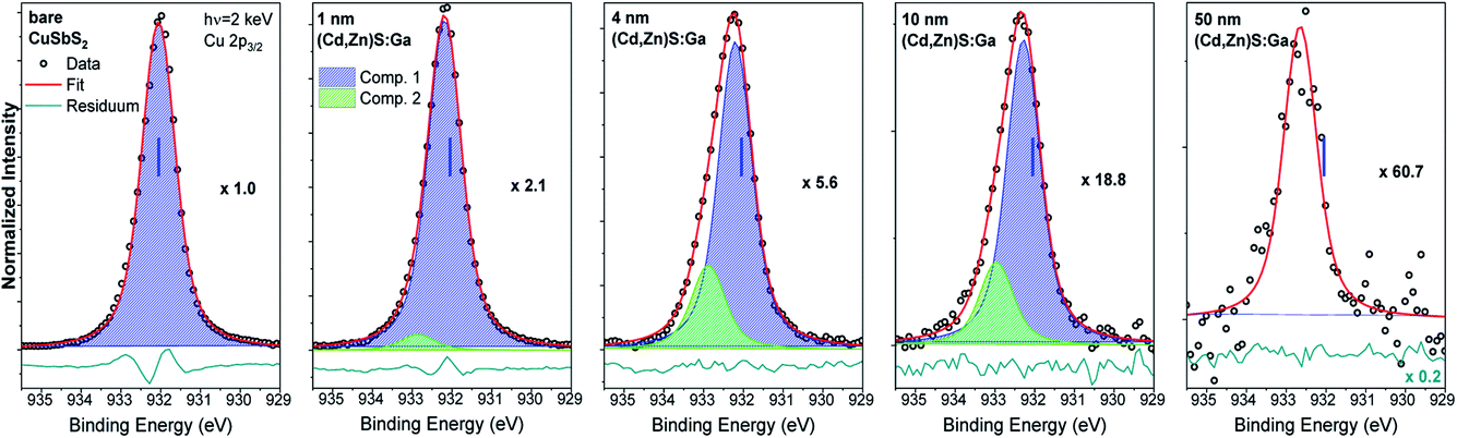 | ||
| Fig. 3 Cu 2p3/2 HAXPES detail spectra recorded with 2 keV of the bare CuSbS2 absorber (leftmost panel) and of the (Cd,Zn)S:Ga/CuSbS2 samples with buffer thicknesses varying from 1 nm (panel second from left) to 50 nm (rightmost panel). Spectra have been normalized to the background at low BE. The background subtracted data is shown together with the fits and resulting residuals (i.e., [data − fit] – shown on different scale if required with scaling factor indicated as e.g., ×0.5). Additionally, the magnification factors are stated (as e.g., ×1.0) that were applied to show all spectra on the same intensity scale as that of the bare absorber. The vertical blue line indicates the BE position of the peak location in the spectrum of the absorber. | ||
Based on the derived intensity of the (main contributions to the) Sb 3d3/2 and Cu 2p3/2 lines, a Cu/(Cu + Sb) ratio of 0.3 is derived for the (surface) composition of the CuSbS2 absorber. This is significantly Cu-deficient compared to the expected (bulk) ratio of 0.5. However, similar Cu-poor surfaces are known to exist for Cu-chalcopyrites.16,17
Fig. 4 shows the Cd 3d5/2 detail spectra of the (Cd,Zn)S:Ga buffer layer thickness series including fit results. As expected, the line intensity increases with increasing buffer layer thickness (as represented by the decreasing magnification factors). For the thin (1 and 4 nm) buffer layers two contributions are required to obtain reasonable fits. For the 10 and 50 nm thick buffer layer samples, only the main contribution (component 1, blue peak) is observed, which we ascribe to the Cd–S bond environment in the (Cd,Zn)S:Ga buffer layer.11 The second component (green peak) is tentatively attributed to Cd in a chemical environment that only exists in close proximity to the buffer/absorber interface. The approximately 1.0 eV BE shift of the Cd 3d5/2 line of the 50 nm (Cd,Zn)S:Ga/CuSbS2 sample (for which the BE positions are indicated as blue vertical lines in the panels of Fig. 4) compared to the 1 nm thick buffer/absorber sample can most likely (and to a large extent) be attributed to sample charging (see Fig. S3† and related discussion).
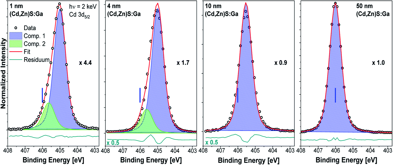 | ||
| Fig. 4 Cd 3d5/2 HAXPES detail spectra recorded with 2 keV of the (Cd,Zn)S:Ga/CuSbS2 samples with buffer thicknesses varying from 1 nm (leftmost panel) to 50 nm (rightmost panel). Spectra have been normalized to the background at low BE. The background subtracted data is shown together with the fits and resulting residuals (i.e., [data − fit] – shown on different scale if required with scaling factor indicated as e.g., ×0.5). Additionally, the magnification factors are stated (as e.g., ×1.0) that were applied to show all spectra on the same intensity scale as that of the 50 nm (Cd,Zn)S:Ga/CuSbS2 sample. The vertical blue line indicates the BE position of the peak location in the spectrum of the thickest buffer sample. | ||
The Zn 2p3/2 spectra of the buffer/absorber samples including fit analysis are shown in Fig. 5. The increase in intensity with increasing (Cd,Zn)S:Ga layer thickness (as represented by the decreasing magnification factor) is expected and similar to that of the Cd 3d5/2 line (see Fig. 4). For the thinner buffer layer samples, namely 1 and 4 nm, two contributions are again required to obtain a reasonable description of the measured data (similar to the Cd 3d5/2 fits). For the thicker buffer layers (10 and 50 nm), the fits reveal a single contribution (component 1, blue peak), which is ascribed to a Zn–S bonding environment in the (Cd,Zn)S:Ga buffer layer.15 The minor contribution (component 2, green peak) is tentatively ascribed to a chemical environment of Zn that is limited to the buffer/absorber interface (similar to component 2 of the Cd 3d5/2 line). The BE shift of the Zn 2p3/2 line of the 50 nm (Cd,Zn)S:Ga/CuSbS2 sample (for which the BE position is indicated with blue vertical lines in the panels of Fig. 5) compared to the 1 nm thick buffer/absorber sample is the same as the one found for the Cd 3d5/2 peak and again (mainly) ascribed to sample charging.
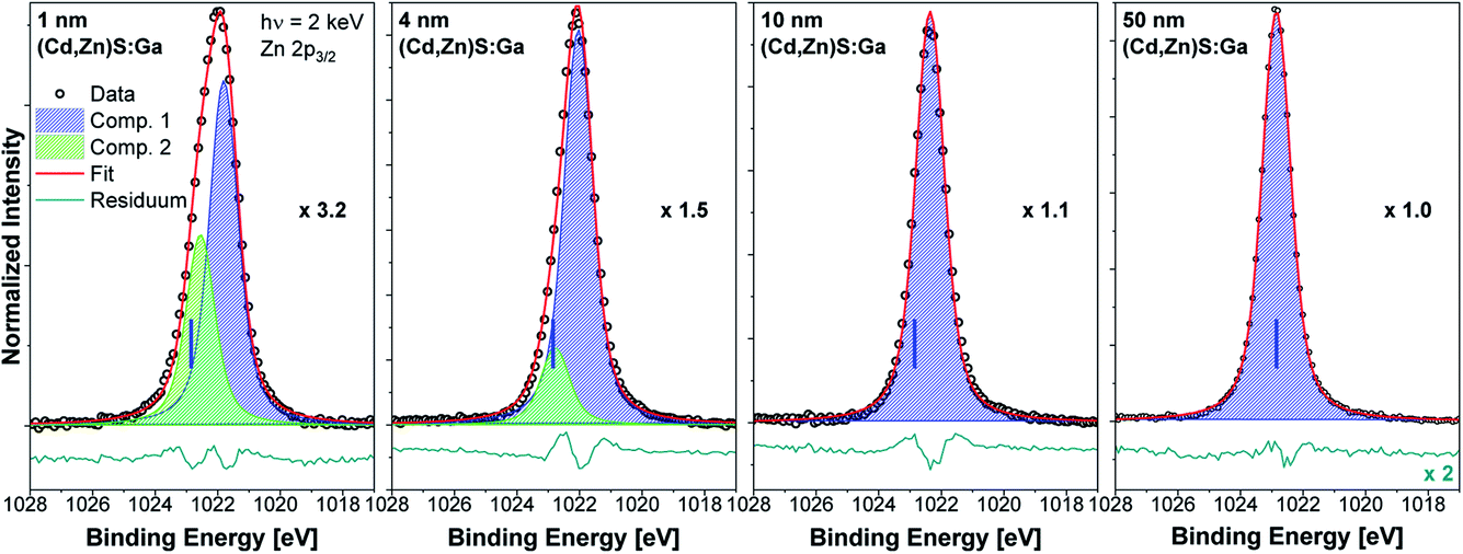 | ||
| Fig. 5 Zn 2p3/2 HAXPES detail spectra recorded with 2 keV of the (Cd,Zn)S:Ga/CuSbS2 samples with buffer thicknesses varying from 1 nm (leftmost panel) to 50 nm (rightmost panel). Spectra have been normalized to the background at low BE. The background subtracted data is shown together with the fits and resulting residuals (i.e., [data − fit] – shown on different scale if required with scaling factor indicated as e.g., ×0.5). Additionally, the magnification factors are stated (as e.g., ×1.0) that were applied to show all spectra on the same intensity scale as that of the 50 nm (Cd,Zn)S:Ga/CuSbS2 sample. The vertical blue line indicates the BE position of the peak location in the spectrum of the thickest buffer sample. | ||
The detail spectra (including fit analysis) of the Ga 2p3/2 line of the buffer/absorber sample set are shown in Fig. S4.† In contrast to the Cd 3d5/2 and Zn 2p3/2 spectra, the Ga 2p3/2 spectra can be fit with one contribution independent of (Cd,Zn)S:Ga thickness, and there is much less intensity variation (note the very similar magnification factors within Fig. S4†), suggesting that Ga does not participate in the chemical interaction which causes the secondary Cd 3d5/2 and Zn 2p3/2 contributions at the buffer/absorber interface but forms a distinct concentration profile within the buffer layer. Also, the BE shift of the Ga 2p3/2 line of the 50 nm (Cd,Zn)S:Ga/CuSbS2 sample (for which the BE positions are indicated as blue vertical lines in the panels of Fig. S4†) compared to the 1 nm thick buffer/absorber sample is smaller (−0.7 eV) than that observed for the other buffer-related core level peaks (i.e., Cd 3d5/2 and Zn 2p3/2) but the same as the shift observed in the C 1s line (that was exclusively attributed to sample charging, see Fig. S3† and related discussion).
For completeness, the S 2p detail spectra of the sample thickness series are shown in Fig. S5.† S is present in the CuSbS2 absorber as well as in the (Cd,Zn)S:Ga buffer layer, resulting in a complex interplay of different spectral features in close energetic proximity. Hence, we deliberately refrain from fitting this region (see related discussion in conjunction with Fig. S5†).
Together with the Cu-diffusion into the buffer layer (see Fig. 3 and related discussion), the presence of the secondary (interface-related) contributions of the Cd 3d5/2 and Zn 2p3/2 lines suggest a significant chemical interaction at the (Cd,Zn)S:Ga/CuSbS2 interface. The diffusion of Cu into the buffer is not surprising and has been extensively studied for CdS18 as well as (Cd,Zn)S19 thin films in the case of Cu2S-based heterojunctions. Also, the diffusion of Cu into sulfide buffer layers is well documented for Cu-chalcopyrites.20,21 In all of these examples, the Cu diffusion is promoted by exposure of the samples to temperatures of around 200 °C – a temperature very similar to the process temperature of the ALD for (Cd,Zn)S:Ga preparation. Cd and Zn are known to diffuse into the upper region of Cu-chalcopyrites when CdS22,23 or Zn-containing24 buffer layers are used (especially at elevated temperatures); the formation of Cd and Zn containing interlayers at CdS/kesterite interfaces has been reported.25 The Cd and Zn diffusion is suggested to be enhanced by copper vacancies,26 and thus the Cu-deficient CuSbS2 surface and the additional Cu diffusion into the buffer layer in our case might especially promote the diffusion of Cd and Zn into the topmost region of the absorber. The different intensity evolution of the secondary (interface-related) Cd 3d5/2 and Zn 2p3/2 contributions might very well be explained by the different diffusion coefficients for Cd27 and Zn28 in Cu-chalcopyrites. The larger diffusion coefficient of Cd compared to that of Zn would predict a higher Zn content in the proximity of the buffer/absorber interface, with Cd more easily diffusing into the CuSbS2.
Based on the derived intensities of the main contributions to the Cd 3d5/2 and Zn 2p3/2 lines, a Zn/(Zn + Cd) ratio of approximately 0.2 is calculated, and it is rather independent of buffer layer thickness (see Fig. 6).
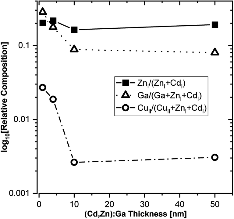 | ||
| Fig. 6 HAXPES derived relative composition of the (Cd,Zn)S:Ga buffer layer as function of thickness. The elemental contributions with a numeral I and II subscript (e.g., ZnI) relate to different fit contributions to the evaluated photoemission lines (see Fig. 2–5): I and II refer to the main contribution (compound I) and to the secondary contribution (compound II), respectively. Ga has no subscript, as Ga 2p3/2 is fitted with one contribution (see Fig. S5†). | ||
Taking the Ga 2p3/2 line and compound 2 of the Cu 2p3/2 line (i.e., the contribution that has been attributed to diffused Cu) into account, also the Ga/(Ga + Zn + Cd) and the Cu/(Cu + Zn + Cd) ratio can be derived. For both ratios, we find a distinct dependence on the buffer layer thickness; with the highest values for the thinnest layers (i.e., close to the buffer/absorber interface), decreasing significantly for thicker buffer layers (see Fig. 6). Close to the interface we find a Ga/(Ga + Zn + Cd) ratio approaching 0.3, exceeding even the Zn/(Zn + Cd) ratio, which then decreases to around 0.08 for the thickest (50 nm) buffer. The Cu/(Cu + Zn + Cd) ratio is approximately one order of magnitude lower, reaching around 0.03 at the interface, decreasing to 0.003 for the 50 nm (Cd,Zn)S:Ga. While the Cu profile of the buffer can be rationalized considering the diffusion process, the Ga profile can presumably be explained by a precursor adsorption that is heavily influenced by the substrate, i.e., a higher sticking coefficient for the bare CuSbS2 compared to that for a (Cd,Zn)S:Ga covered CuSbS2 would be in line with the higher Ga content at the interface.
For insights into the electronic interface structure, the region of the VBM of the bare CuSbS2 and the buffer layer thickness series samples has been measured and the respective spectra are shown in the left panel of Fig. 7. The upper VB of CuSbS2 (black spectrum) is formed mainly by Cu 3d and S 3p derived states.4 With increasing (Cd,Zn)S:Ga buffer layer thickness, the spectral VB shape of the absorber (most prominently the peak 2.5 eV below the Fermi level, EF) is attenuated; the overall shape of the VB evolves into that of the (Cd,Zn)S:Ga buffer for the 50 nm thick buffer layer. This results in a shift of the measured VBM away from EF. For the CuSbS2 absorber, the VBM is derived by linear extrapolation of the leading edge to be (−0.1 ± 0.1) eV. Compared to the VBM positions of related absorber materials (with similar band gap) such as CuInS2 (VBM at (−0.7 … −0.9) eV, depending on the Cu surface content29) or Cu2(Zn,Sn)S4 (VBM at (−0.6 … −0.7 eV), depending on surface treatment30), this VBM position appears to be extraordinarily close to EF. This indicates a significantly higher p-type doping or a less pronounced downwards band bending towards the absorber surface (i.e., veering away from a beneficial conduction type inversion); both effects can have a detrimental impact on charge carrier collection in respective solar cells.31,32
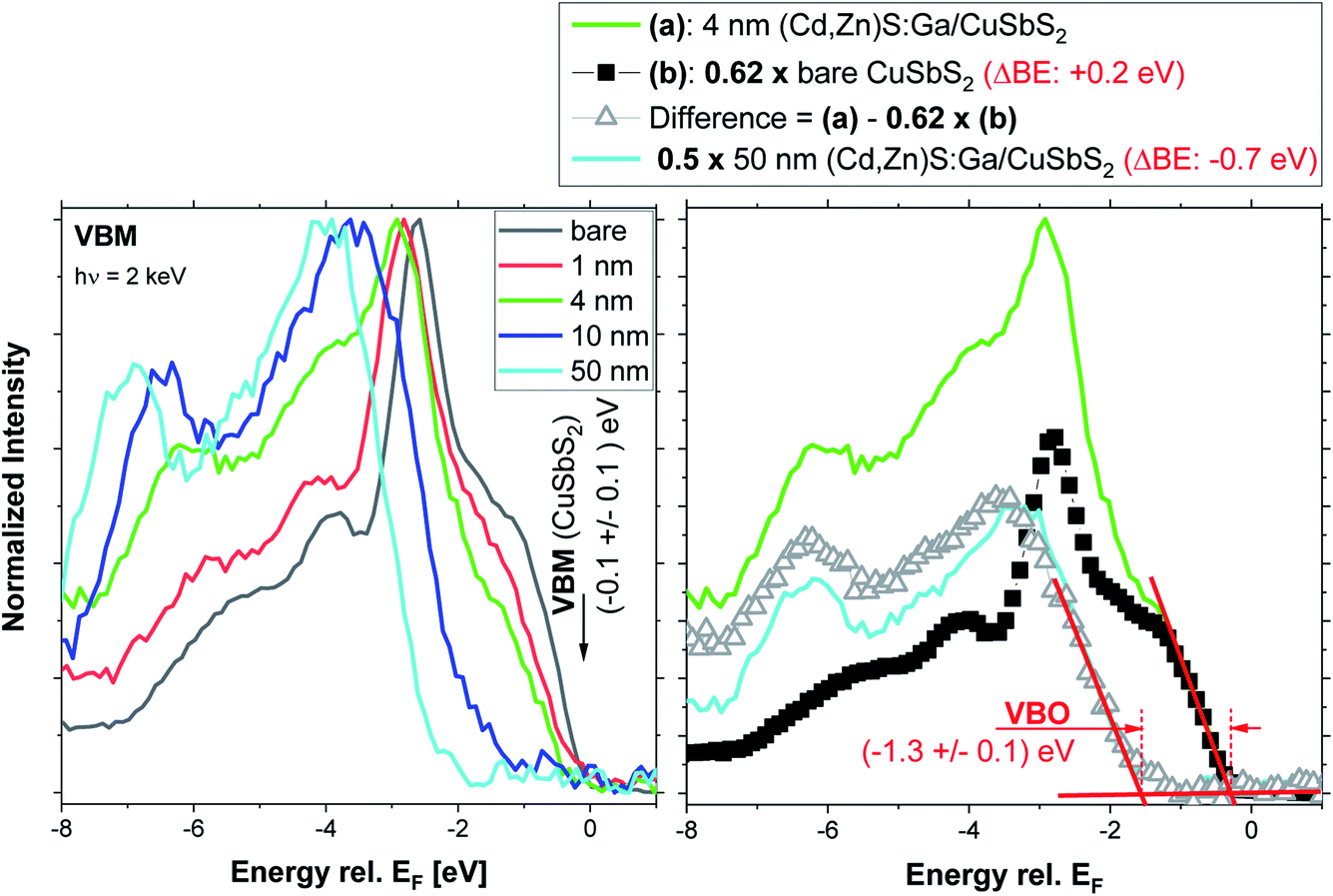 | ||
| Fig. 7 Left panel: normalized HAXPES detail spectra (recorded with 2 keV) of the valence band maximum (VBM) region of the bare CuSbS2 absorber and of the (Cd,Zn)S:Ga/CuSbS2 samples with buffer thicknesses varying from 1 nm to 50 nm. The VBM of the bare absorber (derived by linear extrapolation of the leading edge) is indicated. Right panel: visualization of subtracting the (properly scaled and shifted) spectrum of the bare CuSbS2 absorber (b) from the 4 nm (Cd,Zn)S:Ga/CuSbS2 spectrum (a), resulting in a difference spectrum, representing the buffer related contribution to the VB spectrum. For comparison the (properly scaled and shifted) spectrum of the 50 nm (Cd,Zn)S:Ga/CuSbS2 sample is shown. The linear extrapolation of the leading edges of the (scaled and shifted) spectrum of the bare absorber and of the difference spectrum to derive the VBO is also depicted. | ||
Due to the already discussed charging issues for samples with thick (10 and 50 nm) (Cd,Zn)S:Ga buffer layers (see Fig. S3† and related discussion), we do not follow the conventional approach of deriving the VBM of the 50 nm thick buffer layer sample and subsequent determination of the interface-induced band bending to obtain the VB offset (VBO, see ref. 30 for more details). Instead, we exploit the higher information depth of our HAXPES measurements (compared to conventional photoelectron spectroscopy using ultraviolet light and/or soft X-rays to probe the VBM) and the fact that we study a heterojunction composed of buffer material ((Cd,Zn)S:Ga) with a larger band gap on top of an absorber material (CuSbS2) with a smaller band gap. This configuration ideally allows for HAXPES spectra of the VBM region in which two VB onsets (one for the buffer and one for the absorber) can be observed; as very nicely demonstrated by the VB spectrum of the 4 nm (Cd,Zn)S:Ga/CuSbS2 sample (see green spectrum in the left panel of Fig. 7). The right panel of Fig. 7 shows the subtraction of the bare CuSbS2 absorber spectrum from the spectrum of the 4 nm (Cd,Zn)S:Ga/CuSbS2 sample to isolate the buffer-related contribution of the VB spectrum. To obtain a reasonable difference spectrum, the absorber spectrum had to be scaled by a factor of 0.62 and shifted away from EF (ΔBE = +0.2 eV). Then the derived difference resembles the (properly scaled [×0.5] and shifted [ΔBE = −0.7 eV]) spectrum of the 50 nm (Cd,Zn)S:Ga/CuSbS2 sample quite well. Note that the scaling factor 0.62 is not arbitrary but results from the goal to subtract as much as possible from the CuSbS2 spectrum while not inducing any negative intensity below the (Cd,Zn)S:Ga derived VB onset. The required ΔBE = +0.2 eV shift of the bare CuSbS2 spectrum prior to subtraction agrees very well with the shift observed in the Sb 3d3/2 and Cu 2p3/2 spectra upon deposition of a 4 nm (Cd,Zn)S:Ga buffer layer (see discussion in conjunction with Fig. 2 and 3 above) and thus we ascribe this to a downward band bending of the absorber energy levels upon interface formation. The shift of ΔBE = −0.7 eV required for the spectrum of the 50 nm (Cd,Zn)S:Ga/CuSbS2 sample is, however, attributed to sample charging observed for the thick buffer layer samples (see Fig. S3† and related discussion). By computing the difference in the VBM (obtained by linear extrapolation of the leading edge of the spectrum, see red lines in the left panel of Fig. 5) of the difference spectrum (representing now the buffer-related contribution to the spectrum of the 4 nm (Cd,Zn)S:Ga/CuSbS2 sample) and the VBM of the properly scaled and shifted spectrum of the bare absorber, we derive the VBO at the (4 nm) buffer/absorber interface to be (−1.3 ± 0.1) eV. When the above analytical approach is applied to the 10 nm (Cd,Zn)S:Ga/CuSbS2 interface, the result confirms this VBO estimate (see Fig. S6† and related discussion). The derived VBO values do not have to be additionally corrected for interface-induced band bending effects (as required for the conventional approach) as these are already contained in the combined information of the buffer and absorber VBM in one spectrum. The use of a single measurement also makes this approach rather insensitive to sample charging. Assuming a moderate charging, i.e., no observation of spectral distortions or charge built-up over the course of the measurement, all the spectral features of the combined VBM spectrum should be shifted equally – not affecting the VBO (being a relative difference of two energy levels, any shift will cancel itself out).
In order to estimate the conduction band offset (CBO), we use bulk band gap (Eg) values for CuSbS2 and (Cd,Zn)S:Ga reported in the literature to be 1.5 eV (ref. 15) and 2.45 eV (taken from ref. 5 according to the above derived buffer composition of Cd0.8Zn0.2S), respectively. Then, according to CBO = Ebufferg − Eabsorberg + VBO, a “cliff”-like CBO of approximately −0.35 eV is estimated as depicted in the summarizing scheme in Fig. 8. The derived VBO and CBO values are in reasonable agreement with the energy level offsets for Cd0.8Zn0.2S reported in ref. 5.
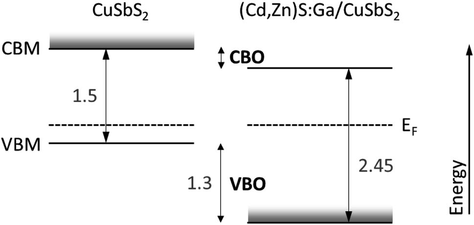 | ||
| Fig. 8 Schematic presentation of the energy levels at the (Cd,Zn)S:Ga/CuSbS2 interface. All values are given in eV. The experimentally derived VBO has an uncertainty of ±0.1 eV. The band gap values of the buffer and absorber are bulk band gaps from literature. The impact of the chemical interaction at the interface or deviation of the surface from the bulk structure is also depicted as shaded grey areas: the Cu diffusion into the buffer will result in the formation of Cu-derived states close to the buffer VBM (potentially pushing the VBM towards EF) and the Cu-deficiency of the CuSbS2 surface will result in an absorber VBM and CBM shift away from EF. The first will result in a reduction of the offset in the VB and the latter will lead to an increase of the negative offset in the CB. | ||
This method assumes that the bulk band gaps also represent the (opto)electronic structure close to the buffer/absorber interface. For CuSbS2 we find a surface composition that is Cu-poor compared to the expected [Cu]![[thin space (1/6-em)]](https://www.rsc.org/images/entities/char_2009.gif) :[Sb]:[S] = 1:1:2 composition (see discussion above). For Cu-chalcopyrites this usually leads to a reduction of the p–d repulsion of the Cu and S derived states that dominate the VB,33 resulting in a VBM shift away from EF. For CuInS2 also a shift of the CBM away from EF could be observed experimentally.29 The potential incorporation of Zn and Cd in the upper region of the absorber is expected to result in a larger band gap as well.
:[Sb]:[S] = 1:1:2 composition (see discussion above). For Cu-chalcopyrites this usually leads to a reduction of the p–d repulsion of the Cu and S derived states that dominate the VB,33 resulting in a VBM shift away from EF. For CuInS2 also a shift of the CBM away from EF could be observed experimentally.29 The potential incorporation of Zn and Cd in the upper region of the absorber is expected to result in a larger band gap as well.
For the (Cd,Zn)S:Ga buffer, we find a Ga-gradient and that Cu is incorporated (see above). The latter will in a first approximation lead to the formation of Cu-derived states close to the VBM, resulting (depending on their concentration) in a related defect level above the VBM within the buffer band gap or in a Cu-derived VBM located much closer to EF. The rather large foot (i.e., the significant deviation of the difference spectra from the linear extrapolation of the leading edge in the VBM region in Fig. 7, right panel or Fig. S6†) might be an indication of the presence of these Cu-derived states. According to ref. 5, Ga (up to a content of 5.5%) does not significantly impact the optical absorption edge – as expected, since gallium sulfide can have a very similar band gap34,35 to the (Cd,Zn)S:Ga buffer used in our study. Thus, in a first approximation we assume that the Ga-gradient has no effect on the energy level positions of the buffer. However, if the amount of Cu incorporation is sufficient to make the buffer VBM Cu-derived, it could lead to a significant reduction of the (negative) VBO, as depicted in Fig. 8. Please note that any impact of (also interface-induced enhanced) Cu-deficiency of the CuSbS2 on the absorber VBM position (due to a reduced p–d repulsion of the S and Cu derived VB states) is directly considered by the applied VBO determination approach (see Fig. 7). The CBO would presumably be most affected by the impact of the interface formation enhanced absorber Cu-deficiency and the potential incorporation of Cd and Zn in the topmost region of the absorber on the CuSbS2 CBM (moving it away from EF), resulting in an increasing (negative) CBO.
In view of its application in solar cells, the energy level offsets at the (Cd,Zn)S:Ga/CuSbS2 interface still suggest the energy level alignment to limit solar cell performance. While the VBO represents a sufficiently high energetic barrier (assuming the buffer VBM is not derived from Cu-derived states), preventing holes from crossing into the emitter, the negative buffer/absorber CBO results in a reduced energetic barrier for charge carrier recombination across the (presumably defect rich) interface.36 This situation becomes even more severe considering the Cu-deficiency related absorber CBM and VBM shift away from EF, as depicted in Fig. 8. To (partially) mitigate this problem the CBM of the buffer layer should be increased, e.g., by increasing the Zn content in the (Cd,Zn)S:Ga buffer.5
Conclusion
The (Cd,Zn)S:Ga/CuSbS2 thin-film solar cell interface was investigated by HAXPES. We find a heavily intermixed interface and a CuSbS2 surface which is significantly Cu-deficient compared to the nominal bulk composition. Cu diffuses from the absorber into the (Cd,Zn)S:Ga buffer layer and Cd and Zn from the buffer interact heavily with the CuSbS2 surface. Ga (from the buffer) and Sb (from the absorber) do not seem to significantly participate in this chemical interaction at the buffer/absorber interface. The buffer exhibits strong Ga and Cu profiles with the highest contents found in the proximity of the buffer/absorber interface. The VBO at this interface could experimentally be derived as (−1.3 ± 0.1) eV despite charging issues. Using bulk band gap energies of the absorber and the buffer from the literature, the CBO could be estimated to be clearly ‘cliff’-like. A Cu-deficiency induced absorber CBM shift away from EF is expected to make this situation more severe, as it will further reduce the energetic barrier for charge carrier recombination across the buffer/absorber interface. Together with the non-ideal electronic structure of the CuSbS2 absorber (indicated by the absorber VBM being too close to EF), this unfavorable energy level alignment at the buffer/absorber interface might be one culprit responsible for the performance limitation of respective solar cells. As mitigation strategies, lowering the doping concentration of the CuSbS2 absorber and increasing the Zn content in the (Cd,Zn)S:Ga buffer are proposed.Conflicts of interest
There are no conflicts to declare.Acknowledgements
The authors thank the HZB for the allocation of synchrotron radiation beamtime. RB acknowledges travel support through the DAAD RISE Professional program. This work was authored in part at the National Renewable Energy Laboratory (NREL), operated by Alliance for Sustainable Energy LLC, for the U.S. Department of Energy (DOE) under contract no. DE-AC36-08GO28308. Funding provided by Office of Science, Basic Energy Sciences. The views expressed in the article do not necessarily represent the views of the DOE or the U.S. Government.References
- M. E. Edley, B. Opasanont, J. T. Conley, H. Tran, S. Y. Smolin, S. Li, A. D. Dillon, A. T. Fafarman and J. B. Baxter, Solution Processed CuSbS2 Films for Solar Cell Applications, Thin Solid Films, 2018, 646, 180–189, DOI:10.1016/j.tsf.2017.12.002.
- S. Banu, S. J. Ahn, S. K. Ahn, K. Yoon and A. Cho, Fabrication and Characterization of Cost-efficient CuSbS2 Thin Film Solar Cells Using Hybrid Inks, Sol. Energy Mater. Sol. Cells, 2016, 151, 14–23, DOI:10.1016/j.solmat.2016.02.013.
- A. Zakutayev, J. D. Major, X. Hao, A. Walsh, J. Tang, T. K. Todorov, L. H. Wong and E. Saucedo, Emerging Inorganic Solar Cell Efficiency Tables (version 2), J. Phys.: Energy, 2021, 3, 032003 CAS.
- T. J. Whittles, T. D. Veal, C. N. Savory, A. W. Welch, F. W. de Souza Lucas, J. T. Gibbon, M. Birkett, R. J. Potter, D. O. Scanlon, A. Zakutayev and V. R. Dhanak, Core Levels, Band Alignments, and Valence-Band States in CuSbS2 for Solar Cell Applications, ACS Appl. Mater. Interfaces, 2017, 9(48), 41916–41926, DOI:10.1021/acsami.7b14208.
- L. L. Baranowski, S. Christensen, A. W. Welch, S. Lany, M. Young, E. S. Toberer and A. Zakutayev, Conduction Band Position Tuning and Ga-Doping in (Cd,Zn)S Alloy Thin Films, Mater. Chem. Front., 2017, 1(7), 1342–1348, 10.1039/c6qm00291a.
- A. W. Welch, L. L. Baranowski, P. Zawadzki, C. DeHart, S. Johnston, S. Lany, C. A. Wolden and A. Zakutayev, Accelerated Development of CuSbS2 Thin Film Photovoltaic Device Prototypes, Prog. Photovoltaics Res. Appl., 2016, 24(7), 929–939, DOI:10.1002/pip.2735.
- A. W. Welch, P. P. Zawadzki, S. Lany, C. A. Wolden and A. Zakutayev, Self-regulated growth and tunable properties of CuSbS2 solar absorbers, Sol. Energy Mater. Sol. Cells, 2015, 132, 499–506, DOI:10.1016/j.solmat.2014.09.041.
- M. Gorgoi, S. Svensson, F. Schäfers, G. Öhrwall, M. Mertin, P. Bressler, O. Karis, H. Siegbahn, A. Sandell, H. Rensmo, W. Doherty, C. Jung, W. Braun and W. Eberhardt, The High Kinetic Energy Photoelectron Spectroscopy Facility at BESSY Progress and First Results, Nucl. Instrum. Methods Phys. Res., Sect. A, 2009, 601(1–2), 48–53, DOI:10.1016/j.nima.2008.12.244.
- F. Schaefers, M. Mertin and M. Gorgoi, KMC-1: A High Resolution and High Flux Soft X-Ray Beamline at BESSY, Rev. Sci. Instrum., 2007, 78(12), 123102, DOI:10.1063/1.2808334.
- M. P. Seah, I. S. Gilmore and S. J. Spencer, XPS: Binding Energy Calibration of Electron Spectrometers 4—Assessment of Effects for Different X-Ray Sources, Analyser Resolutions, Angles of Emission and Overall Uncertainties, Surf. Interface Anal., 1998, 26(9), 617–641, DOI:10.1002/(sici)1096-9918(199808)26:9<617::aid-sia407>3.0.co;2-v.
- Unifit – Analysis Software for Photoelectron Spectroscopy (XPS), X-Ray Absorption Spectroscopy (XAS), Auger Electron Spectroscopy (AES) and RAMAN Spectroscopy, https://home.uni-leipzig.de/unifit/, accessed Aug. 27, 2018.
- M. B. Trzhaskovskaya, V. I. Nefedov and V. G. Yarzhemsky, Photoelectron Angular Distribution Parameters for Elements Z=1 to Z=54 in the Photoelectron Energy Range 100–5000 eV, At. Data Nucl. Data Tables, 2001, 77(1), 97–159, DOI:10.1006/adnd.2000.0849.
- M. B. Trzhaskovskaya, V. I. Nefedov and V. G. Yarzhemsky, Photoelectron Angular Distribution Parameters for Elements Z=55 to Z=100 in the Photoelectron Energy Range 100–5000 eV, At. Data Nucl. Data Tables, 2002, 82(2), 257–311, DOI:10.1006/adnd.2002.0886.
- QUASES-IMFP-TPP2M – QUASES, http://www.quases.com/products/quases-imfp-tpp2m/, accessed Nov. 30, 2020.
- C. D. Wagner, The NIST X-Ray Photoelectron Spectroscopy (XPS) Database, 76.
- J. R. Tuttle, D. S. Albin and R. Noufi, Thoughts on the microstructure of polycrystalline thin film CuInSe2 and its impact on material and device performance, Sol. Cells, 1991, 30, 21, DOI:10.1016/0379-6787(91)90034-m.
- D. Schmid, M. Ruckh, F. Grunwald and H.-W. Schock, Chalcopyrite/defect chalcopyrite heterojunctions on the basis of CuInSe2, J. Appl. Phys., 1993, 73, 2902, DOI:10.1063/1.353020.
- H. C. Hsieh, The effect of Cu diffusion in a Cu2S/CdS heterojunction solar cell, J. Appl. Phys., 1982, 53, 1727, DOI:10.1063/1.331640.
- L. C. Burton, P. N. Uppal and D. W. Dwight, Cross diffusion of Cd and Zn in Cu2S formed on ZnxCd1−xS thin films, J. Appl. Phys., 1982, 53, 1538, DOI:10.1063/1.330654.
- S. Spiering, A. Eicke, D. Hariskos, M. Powalla, N. Naghavi and D. Lincot, Large-area Cd-free CIGS solar modules with In2S3 buffer layer deposited by ALCVD, Thin Solid Films, 2004, 451–452, 562–566, DOI:10.1016/j.tsf.2003.10.090.
- M. Bär, N. Barreau, F. Couzinié-Devy, S. Pookpanratana, J. Klaer, M. Blum, Y. Zhang, W. Yang, J. D. Denlinger, H.-W. Schock, L. Weinhardt, J. Kessler and C. Heske, Nondestructive depth-resolved spectroscopic investigation of the heavily intermixed In2S3/Cu(In,Ga)Se2 interface, Appl. Phys. Lett., 2010, 96, 184101, DOI:10.1063/1.3425739.
- D. Liao and A. Rockett, Cd doping at the CuInSe2/CdS heterojunction, J. Appl. Phys., 2003, 93, 9380, DOI:10.1063/1.1570500.
- T. Nakada and A. Kunioka, Direct evidence of Cd diffusion into Cu(In,Ga)Se2 thin films during chemical-bath deposition process of CdS films, Appl. Phys. Lett., 1999, 74, 2444, DOI:10.1063/1.123875.
- J.-H. Wi, T. G. Kim, J. W. Kim, W.-J. Lee, D.-H. Cho, W. S. Han and W. D. Chung, Photovoltaic Performance and Interface Behaviors of Cu(In,Ga)Se2 Solar Cells with a Sputtered-Zn(O,S) Buffer Layer by High-Temperature Annealing, ACS Appl. Mater. Interfaces, 2015, 7(31), 17425–17432, DOI:10.1021/acsami.5b04815.
- M. Bär, I. Repins, L. Weinhardt, J.-H. Alsmeier, S. Pookpanratana, M. Blum, W. Yang, C. Heske, R. G. Wilks and R. Noufi, Zn–Se–Cd–S Interlayer Formation at the CdS/Cu2ZnSnSe4 Thin-Film Solar Cell Interface, ACS Energy Lett., 2017, 2(7), 1632–1640, DOI:10.1021/acsenergylett.7b00140.
- F. Werner, F. Babbe, J. Burkhart, C. Spindler, H. Elanzeery and S. Siebentritt, Interdiffusion and Doping Gradients at the Buffer/Absorber Interface in Thin-Film Solar Cells, ACS Appl. Mater. Interfaces, 2018, 10(34), 28553–28565, DOI:10.1021/acsami.8b08076.
- K. Hiepko, J. Bastek, R. Schlesiger, G. Schmitz, R. Wuerz and N. A. Stolwijk, Diffusion and incorporation of Cd in solar-grade Cu(In,Ga)Se2 layers, Appl. Phys. Lett., 2011, 99, 234101, DOI:10.1063/1.3665036.
- J. Bastek, N. A. Stolwijk, R. Wuerz, A. Eicke, J. Albert and S. Sadewasser, Zinc diffusion in polycrystalline Cu(In,Ga)Se2 and single-crystal CuInSe2 layers, Appl. Phys. Lett., 2012, 101, 074105, DOI:10.1063/1.4745927.
- M. Bär, J. Klaer, L. Weinhardt, R. G. Wilks, S. Krause, M. Blum, W. Yang, C. Heske and H.-W. Schock, Cu2-xS Surface Phases and Their Impact on the Electronic Structure of CuInS2 Thin Films – A Hidden Parameter in Solar Cell Optimization, Adv. Energy Mater., 2013, 3, 777–781, DOI:10.1002/aenm.201200946.
- M. Bär, B.-A. Schubert, B. Marsen, R. G. Wilks, S. Pookpanratana, M. Blum, S. Krause, T. Unold, W. Yang, L. Weinhardt, C. Heske and H.-W. Schock, Cliff-like conduction band offset and KCN-induced recombination barrier enhancement at the CdS/Cu2ZnSnS4 thin-film solar cell heterojunction, Appl. Phys. Lett., 2011, 99, 222105, DOI:10.1063/1.3663327.
- A. V. Sachenko, V. P. Kostylyov, M. V. Gerasymenko, R. M. Korkishko, M. R. Kulish, M. I. Slipchenko, I. O. Sokolovskyi and V. V. Chernenko, Analysis of the silicon solar cells efficiency. Type of doping and level optimization, Semicond. Phys., Quantum Electron. Optoelectron., 2016, 19(1), 067–074, DOI:10.15407/spqeo19.01.067.
- R. Klenk, Characterisation and modelling of chalcopyrite solar cells, Thin Solid Films, 2001, 387(1–2), 135–140, DOI:10.1016/s0040-6090(00)01736-3.
- S.-H. Wei and A. Zunger, Band offsets and optical bowings of chalcopyrites and Zn-based II–VI alloys, J. Appl. Phys., 1995, 78, 3846, DOI:10.1063/1.359901.
- E. Aulich, J. L. Brebner and E. Mooser, Indirect Energy Gap in GaSe and GaS, Phys. Status Solidi B, 1969, 31(1), 129–131, DOI:10.1002/pssb.19690310115.
- M. Isik, N. M. Gasanly and L. Gasanova, Spectroscopic ellipsometry investigation of optical properties of β-Ga2S3 single crystals, Opt. Mater., 2018, 86, 95–99, DOI:10.1016/j.optmat.2018.09.049.
- R. Scheer, Activation Energy of Heterojunction Diode Currents in the Limit of Interface Recombination, J. Appl. Phys., 2009, 105, 104505, DOI:10.1063/1.3126523.
Footnote |
| † Electronic supplementary information (ESI) available. See https://doi.org/10.1039/d2fd00056c |
| This journal is © The Royal Society of Chemistry 2022 |