
 Open Access Article
 This Open Access Article is licensed under a Creative Commons Attribution-Non Commercial 3.0 Unported Licence
Versatile near-infrared polarization-sensitive ionic liquid-gated organic electrochemical phototransistor†
Jia Li,
Xingyu Zhang,
Min Guo,
Xinmu Chen,
Xiaolong Li,
Zhidong Lou ,
Yanbing Hou,
Feng Teng* and
Yufeng Hu*
,
Yanbing Hou,
Feng Teng* and
Yufeng Hu*
Key Laboratory of Luminescence and Optical Information, Ministry of Education, Institute of Optoelectronic Technology, Beijing Jiaotong University, Beijing, 100044, P. R. China. E-mail: yfhu@bjtu.edu.cn; fteng@bjtu.edu.cn
First published on 27th May 2025
Abstract
In response to the rising demand for diversified detection capabilities, multi-dimensional and multi-functional optoelectronic devices have become a significant focus in scientific research. The organic electrochemical phototransistor (OECPT) is a pioneering photoelectric conversion device whose unique operating mechanism positions it as a strong candidate for applications in areas such as biological systems, sensing, and artificial neural network modeling. In this study, polarization-responsive OECPT devices were fabricated by combining thermally oriented anisotropic thin films with ionic liquid gating. The resulting devices demonstrated a distinct polarization sensitivity in the near-infrared region, achieving a photogenerated current dichroic ratio of 1.52. Furthermore, by modulating device non-volatility vis gate voltage, we explored the potential of OECPTs in neural synapse emulation and optoelectronic memory storage. These findings provide valuable insights for advancing the design and application of polarization-sensitive OECPT devices in multifunctional optoelectronic systems.
Introduction
In response to the rapid advancements in science and technology, the replacement cycle for electronic devices has significantly shortened, necessitating continuous improvement in the performance of core electronic components. Key areas of focus include ensuring high reliability, multifunctionality, and minimal energy consumption.1–3 These goals demand concerted research and development efforts aimed at pushing the boundaries of current technologies. Among emerging devices, organic phototransistors (OPTs) stand out as promising optoelectronic devices, leveraging semiconductor materials with photosensitive properties to replace conventional conductive channel layers.4,5 This substitution enables OPTs to generate light-responsive current signals, with gate modulation offering effective noise suppression, signal amplification, and additional storage functions based on the dielectric layer.6 These properties have positioned OPTs at the forefront of research, promising new applications in fields such as photodetection,7,8 photoelectric storage,9,10 and neural simulation.11–14 Traditional transistors, however, face limitations due to their high operating voltage, motivating research into various approaches to overcome these constraints. Innovations have included the use of high-dielectric-constant materials,15,16 reduced device charge trap density,17,18 dynamic voltage regulation,19 and the exploration of novel transistor structures.20–22One such approach is the organic electrochemical transistor (OECT),23 a three-terminal device introduced in the 1980s that utilizes an electrolyte layer with mobile ions as a gate-regulation medium.24 Unlike conventional field-effect transistors, OECTs rely on ion-mediated gate field modulation to control charge transport in the channel. The distinctive properties of the electric double layer (EDL) formed by ions in the OECTs enable reduced gate dielectric thickness (nanometer level), resulting in notable low operating voltages. The flexibility in selecting gate electrolytes for OECTs also enables biocompatibility, environmental compatibility, and cost-effectiveness,25,26 expanding potential applications in environmental monitoring,27 photodetection,28 and biomedical fields.29,30
Combining a photosensitive channel layer with an OECT structure leads to organic electrochemical phototransistors (OECPTs), which exhibit high photo-responsivity under low-voltage operation. Researchers have achieved notable advances in OECPT design. Lhuillier et al. in 2014 synthesized CdSe/CdS nanosheets with a core/shell structure for use as a photoactive semiconducting layer in an electrochemical transistor, achieving a responsivity of approximately 10 mA W−1 at an operating voltage below than 2 V.31 In 2017, Xu et al. developed large-capacitance ionic gels to serve as gate electrolytes in a bulk heterojunction (BHJ)-based OECPT, resulting in a maximum responsivity of approximately 1.5 × 10³ A W−1.32 In 2019, Lan et al. demonstrated an OECPT device that achieved a maximum responsivity of 7.3 A W−1 under the illumination of a sunlight simulator.33 In 2022, Sun et al. showcased a responsivity of 3.56 A W−1 for an OECPT when exposed to near-infrared light, with potential applications in erasable photoelectric storage devices.34 By 2023, Yang et al. further improved OECPT technology to create a stretchable, ultrasensitive, low-energy phototransistor capable of real-time human pulse monitoring.35 In 2024, Lin et al. reported that the OECPT, designed as an electrical double-layer transistor (EDLT), exhibited an extremely low energy consumption of just 0.59 nW, along with a responsivity of up to 6.12 A W−1.36 The relevant properties of the above devices are listed in Table 1 for comparison.
| Active layer material | Electrolyte material | Response wavelength | Responsivity | Reference |
|---|---|---|---|---|
| CdSe/CdS nanosheets | LiClO4: PEG | 405 nm | 10 mA W−1 | 31 |
| PDPP2T: PC61BM | P(VDF-HFP): [EMIM][TFSI] | 808 nm | 1.5 × 10³ A W−1 | 32 |
| PCDTBT | [EMIM][TFSI] | Sunlight | 7.3 A W−1 | 33 |
| PCDTPT | [EMIM][TFSI] | 885 nm | 3.56 A W−1 | 34 |
| SEBS: PDPP2T: PC61BM | P(VDF-HFP): [EMIM][TFSI]: LiTFSI | 808 nm | 2 × 10³ A W−1 | 35 |
| DNTT | Indigo carmine: P4VP-b-PEO | 450 nm | 6.12 A W−1 | 36 |
The recent development of polarized light detectors enhances light polarization detection beyond intensity and wavelength, allowing devices to distinguish between linear and circular polarizations based on anisotropic optical absorption.37 In 2011, anisotropic absorption in poly(3-hexylthiophene) (P3HT) films was achieved by Yang et al. through the application of unidirectional thermal rubbing.38 The resulting photodetector exhibited an electric current dichroic ratio (DRI) of 3.54. Subsequently, various film fabrication methods, such as blade-coating,39,40 off-center spin-coating,41,42 unidirectional floating film transfer method,43–46 and strain-induced orientation,47–49 have been employed to impart polarization sensitivity to polymer films, leading to advances in polarization-sensitive photodetectors. However, further research is required to fully integrate electrochemical phototransistors with polarization detection.
In this work, oriented poly[[1,2,5]thiadiazolo[3,4-c]pyridine-4,7-diyl (4,4-dihexadecyl-4H-clopenta[2,1-b:3,4-b′]-dithiophene-2,6-diyl)[1,2,5] thiadiazolo[3,4-c]pyridine-7,4-diyl(4,4-dihexadecyl-4H-cyclopenta [2,1-b,3,4-b′]dithiophene-2,6-diyl)] (PCDTPT) films with dichroic optical absorption were prepared using thermal rubbing orientation. These films were then integrated into an electrochemical transistor with a top-gate-bottom-contact configuration and an ionic liquid ([EMIM][TFSI]) as the gate electrolyte. This approach enables the creation of polarization-sensitive electrochemical phototransistors capable of distinguishing linearly polarized light, exhibiting distinct photocurrent response to different polarization angles. While ordering the polymer backbone through rubbing orientation is a common method for preparing oriented aligned layers, most of the existing studies have focused only on the change in mobility and oriented films' performance in two-terminal devices.50–52 In contrast, this work applies oriented polymer films to ionic liquid-gated electrochemical transistors and explores their device performance. The resulting electrochemical phototransistor devices exhibit a significant anisotropic photoelectric response. Although the gating results are somewhat routine, the novel aspect lies in the device's distinct response to incident light at different polarization angles. Furthermore, the non-volatile nature of the optical response shows a clear dependence on the gate voltage. In conclusion, this work may offer valuable insights for the development of novel multifunctional optoelectronic devices that integrate anisotropic thin films with electrolyte-gated electrochemical phototransistors.
Experimental section
Materials
The gate electrolyte material, 1-ethyl-3-methylimidazolium bis(trifluoromethylsulfonyl)imide ([EMIM][TFSI], C8H11F6N3O4S2, 99%), was obtained from Innochem. The active layer material, PCDTPT (MW = 75![[thin space (1/6-em)]](https://www.rsc.org/images/entities/char_2009.gif) 000), was sourced from 1-material. Chloroform (CH3Cl, >99.8%) was purchased from Amethyst Chemicals. Custom-designed patterned indium tin oxide (ITO, ∼135 nm thick, ≤15 Ω square resistance) glass substrates were provided by South China Science & Technology Co. Ltd, while velvet fabric for rubbing orientation was obtained from Taobao. All materials were used as received without further treatment.
000), was sourced from 1-material. Chloroform (CH3Cl, >99.8%) was purchased from Amethyst Chemicals. Custom-designed patterned indium tin oxide (ITO, ∼135 nm thick, ≤15 Ω square resistance) glass substrates were provided by South China Science & Technology Co. Ltd, while velvet fabric for rubbing orientation was obtained from Taobao. All materials were used as received without further treatment.
Fabrication of the oriented PCDTPT film
A 10 mg mL−1 chloroform solution of PCDTPT was stirred overnight at 60 °C under a nitrogen atmosphere to ensure complete dissolution. Substrate was subjected to ultrasonic cleaning for 20 min in ITO cleaner, deionized water, and anhydrous ethanol, sequentially, and then dried under nitrogen flow. Prior to spin-coating, substrates were treated in a vacuum oxygen plasma cleaner to remove surface residues. The film was then spin-coated at an acceleration of 1000 rpm s−1 and a rotation speed of 2000 rpm for 60 s within a nitrogen-filled glovebox. Following spin-coating, the PCDTPT film-coated substrate was annealed at 200 °C on a hot plate for 8 min to enhance crystallinity. The device was then placed in a fixed groove mold and annealed at 220 °C (slightly higher than the annealing temperature38) for 1 min. Subsequently, the film was gently rubbed unidirectionally using velvet fabric for approximately 1 min. A final post-annealing treatment was performed for 3 min.Device fabrication
Pre-deposited patterned ITO electrodes on glass substrate served as the source and drain electrodes, with a channel length (L) of 50 μm and width (W) of 1000 μm. The oriented PCDTPT film was fabricated as described. Device assembly was carried out in a nitrogen-filled glovebox. For testing, approximately 2.5 μL of [EMIM][TFSI] ionic liquid was applied atop the conducting channel as the gate electrolyte layer, ensuring full coverage of the channel with a large contact angle. A tungsten probe, inserted into the [EMIM][TFSI] droplet, was used as the gate electrode to apply gate bias voltage.Characterization
Substrate surface cleaning was conducted using a vacuum oxygen plasma cleaning machine (TS-PL02, Shenzhen Tonson Tech Automation Equipment Co., Ltd). Film absorption spectra were measured with an Ocean Optics USB4000 spectrometer, using a DH-2000-BAL deuterium-halogen light source. Film surface morphology characterization was performed using atomic force microscopy (Cypher, VRS). Characterization of the organic polarization-sensitive electrochemical phototransistor was carried out using a semiconductor analyzer (Keithley 4200 SCS). A self-assembled coaxial incident light system was used, consisting of a near-infrared LED light source (Oeabt, LED-D1-850), a polarizer (Daheng Optics, GLC-051012), and an electrically driven rotation stage (LETEK, ICSM-RT1). Incident light intensity was calibrated with an OPHIR Photonics PD300-UV-ROHS power meter.Results and discussion
The molecular structures of the materials are illustrated in Fig. 1a. PCDTPT was selected as the active layer material due to its exceptional light absorption and exciton dissociation properties, functioning effectively as a donor–acceptor copolymer. Its infrared response range also demonstrates significant potential for signal sensing applications. Additionally, PCDTPT functions as a P-type semiconductor with notable charge carrier mobility. Consequently, it combines efficient photoconversion capabilities with high charge transport, making it suitable as the active layer in the OECPT devices. [EMIM][TFSI], a commonly utilized ionic liquid, is capable of forming electric double layers at the semiconductor interface with a unit area capacitance of approximately 10 nF cm−2.33 This ionic liquid also exhibits high ionic conductivity, which enables rapid ion migration in response to electric field changes. Furthermore, [EMIM][TFSI] possesses excellent stability under ambient conditions, low volatility, and environmental compatibility, rendering it a suitable choice as the gate electrolyte material.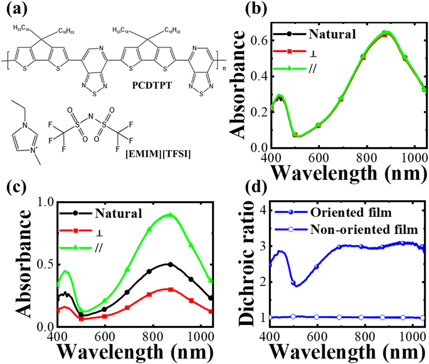 | ||
| Fig. 1 (a) Molecular structures of PCDTPT and [EMIM][TFSI]. Absorption spectra of PCDTPT thin films (b) before and (c) after orientation treatment under varying polarization states of incident light, where “⊥” represents light polarized perpendicular to the film's rubbing alignment direction, and “‖” represents light polarized parallel to the alignment direction. (d) Comparison of optical absorption dichroic ratio between oriented and non-oriented thin films. | ||
The polarized absorption spectra of PCDTPT films, before and after orientation treatment, are depicted in Fig. 1b and c, respectively. The non-oriented film exhibits optically isotropic properties, as reflected in its polarized absorption spectrum. Conversely, the oriented PCDTPT film demonstrates distinct absorption characteristics depending on the polarization state of the incident light. For incident light polarized parallel to the rubbing direction (referred to as parallel light), higher absorbance is observed, whereas lower absorbance is recorded for incident light polarized perpendicular to this direction (referred to as perpendicular light). This phenomenon occurs because the randomly arranged polymer chain segments in the film attain a certain degree of order after uniaxial orientation. The film preferentially absorbs light with polarization parallel to the main chain, even surpassing the absorbance of unpolarized light. This intrinsic mechanism accounts for the polarization sensitivity observed in oriented organic polymer films. Following orientation treatment, the film's thickness is reduced due to the rubbing process, resulting in lower absorbance for unpolarized light compared to non-oriented films. The dichroic ratio (DR) is employed to quantify the film's optical anisotropy and is defined as follows:
| DR = Amax/Amin | (1) |
Atomic force microscope (AFM) characterization was performed to further compare the morphology of the PCDTPT films before and after orientation. The results for the non-oriented film are shown in Fig. 2a. The film's surface is flat and free of significant structural defects, with a root mean square (RMS) surface roughness of only 3.402 nm. Overall, no ordered orientational arrangement is observed in the non-oriented films. In contrast, the oriented film demonstrates clear alignment of polymer chains, as coarse, fiber-like aggregates are evident in AFM images of the film's surfaces (Fig. 2b). These unidirectionally aligned polymer backbones contributed to anisotropic absorption in the films. However, it is noteworthy that the morphology of the oriented film was compromised due to the mechanically destructive nature of velvet friction orientation, which increases the RMS roughness to 23.985 nm and created an uneven film surface. This morphological change is observed to hinder both carrier transport and gate modulation within the film.
 | ||
| Fig. 2 Surface morphology of PCDTPT thin films observed using AFM: (a) before and (b) after orientation treatment by rubbing. The red arrow indicates the rubbing direction for orientation. | ||
The OECPT device was designed with a top-gate-bottom-contact structure, as shown in Fig. 3a. Due to the limited dependence of the electrochemical working mechanism on electrode materials, pre-deposited patterned ITO (with a work function of 4.7 eV)34 was employed as the materials for source and drain electrodes thus simplifying the fabrication process. The dimensions of the conducting channel are W/L = 1000/50 μm. The channel was fully covered by [EMIM][TFSI], ensuring effective gate modulation across the entire channel. Subsequently, electrical characterization of the device under various illumination conditions was conducted in ambient atmosphere with a fixed source-drain voltage (VDS) of −0.8 V. The transfer characteristics are compared in Fig. 3c. The device exhibits typical P-type transistor characteristics. In comparison to the non-oriented device (Fig. 3b), the oriented device shows a decrease in modulation performance, attributed to morphological damage in the film caused by the orientation process, which adversely impact charge transport. In OECT, maximum transconductance (gm) is commonly used to evaluate device performance and is defined as follows:
 | (2) |
 | ||
| Fig. 3 (a) Schematic of the OECPT device structure. Transfer curves of (b) the non-oriented device and (c) the oriented device, with VDS = −0.8 V under a constant 1 mW cm−2 incident light intensity at 850 nm. (d) Comparison of transconductances values between the two device types. | ||
The dichroic ratio of photocurrent, DRIP, is an optoelectronic parameter used to quantify the dichroism of photogenerated currents. This ratio can be derived from the transfer characteristics and is defined as:
 | (3) |
 | (4) |
 | (5) |
 | ||
| Fig. 4 (a) Photogenerated current dichroic ratio (DRIP), (b) responsivity (R), and (c) normalized detectivity (D*) of the oriented device. (d) Corresponding optoelectronic performance parameters for the non-oriented device. | ||
| Oriented device | Non-oriented device | ||
|---|---|---|---|
| Ion/Ioff | 6.43 × 101 | 1.99 × 10² | |
| Vth | 0.45 V | 0.21 V | |
| gm | 2.25 × 10⁻⁷ S | 3.29 × 10⁻⁶ S | |
| R | ‖ | 84.92 mA W−1 | 2.72 A W−1 |
| ⊥ | 44.12 mA W−1 | ||
| D* | ‖ | 1.14 × 10¹⁰ Jones | 1.24 × 10¹¹ Jones |
| ⊥ | 5.66 × 10⁹ Jones | ||
To assess the performance stability of the devices, approximately 20 randomly selected devices, both oriented and non-oriented, were tested. The electrical parameters, such as threshold voltage, on-state current, off-state current, and the on/off ratio, were extracted from their transfer curves (ESI Fig. S1†). The results indicate that, following the friction orientation treatment, the threshold voltage of the devices exhibits a wider fluctuation range, and the overall on/off ratio decreases. This behavior is attributed to the disruption of the film morphology. A comparison of these results is provided in Table S1.† These findings are consistent with previous studies. For further investigation into device stability, the variation in current at steady-state voltage was also analyzed (ESI Fig. S2†). The data show that non-oriented devices exhibit more stable off-state currents, which remain nearly constant for over 500 seconds. However, the on-state current continues to increase without reaching saturation within a short period. This phenomenon is attributed to the unique electrochemical working mechanism of organic electrochemical transistors (OECTs). Over time, removable ions migrate into the channel, which continuously enhances channel conductance, thereby leading to a gradual increase in on-state current. In contrast, electrochemical processes in oriented devices are more susceptible to perturbations due to the altered film morphology, which leads to both on- and off-state currents increasing with time. While device stability has been demonstrated to some extent, there remains room for improvement, which we plan to address in future work.
Fig. 5(a) and (b) illustrate the device's operation in the dark. When a positive gate voltage is applied, the cations [EMIM]+ in the ionic liquid are driven by the electric field toward the interface between the electrolyte and semiconductor layers. This induces electronic changes within the semiconductor layer, forming an electric double layer structure. The resulting increase in localized electron concentration is accompanied by hole depletion, which reduces hole conductivity and hinders the transport of holes injected from the source. Consequently, the device exhibits a low IDS under positive gate voltage.
 | ||
| Fig. 5 Schematic of the device operation mechanism. (a) and (b) Are in the dark conditions. (c) and (d) Are in the light condition. | ||
As the gate voltage shifts to a more negative value, hole channels with higher hole concentration gradually form at the interface. This facilitates a high-conductance path for the injected holes, resulting in the device turning on and an increase in IDS. Fig. 5(c) and (d) show the operating mechanism of the device under light. Upon illumination, photogenerated electrons and holes are created within the semiconductor layer. Some of these carriers contribute to channel formation, while others are transported as free charges. This leads to an enhancement in IDS compared to the dark state, due to the additional carriers generated by the light. Notably, in the pre-on state, the device exhibits higher responsivity. This is because the photogenerated current is suppressed under positive gate voltage, while at negative gate voltage, the channel current is primarily dominated by the injected current due to gate amplification. As a result, the device achieves maximum responsivity around VDS = 0 V.
The dependence of the device's response on the incident light polarization angle was evaluated under constant bias conditions. In electrochemical transistors, unavoidable ion permeation typically occurs during operation, wherein ions diffuse into the active layer driven by a concentration gradient, thereby initiating a series of electrochemical redox reactions that generally increase the channel conductivity. Conversely, the on-state voltage facilitates ion migration into the active layer, enhancing conductivity and causing the channel current to increase over time, a factor that is not conducive to polarization detection by the device. Consequently, the operating region for electrochemical phototransistors is typically confined to the off-state region of the device. For polarized light response testing in this work, a constant bias voltage of VDS = −0.8 V and VG = 1 V was applied to the device. The active area was illuminated with incident light at 850 nm, with an intensity of 1 mW cm−2. The resulting current signals under parallel and perpendicular polarization of light, shown in Fig. 6a, reveal a light response in the nA range, with significant differences observed between responses to parallel and perpendicular light. The photocurrent dichroic ratio DRIP under these two illumination conditions is approximately 1.52, which is slightly lower than the value derived from transfer curves at the same voltage. This outcome is attributed to the suppression of the total current flowing through the channel by the off-state gate voltage, which, although it stabilizes the light response under the constant off-state bias, results in a smaller overall light response and a decrease in DRIP value.
 | ||
| Fig. 6 (a) Device performance under constant bias (VDS = −0.8 V, VG = 1 V) with varied illumination conditions. (b) Dynamic response of device current to continuously changing incident light polarization angles under constant bias. (c) Polar coordinate plot of the response, with blue dots representing experimental data and the red dashed line indicating the theoretical curve. θ denotes the angle between the incident light polarization and the device orientation. (d) Polarized light response curve with bias condition adjusted to VG = 0.5 V. | ||
The dependence of the device's response on the polarization angle of incident light is illustrated in Fig. 6b, where an electrically-driven rotating polarizer was employed to modulate the light's polarization angle. Real-time monitoring of current changes under constant bias conditions shows results consistent with Malus' law, as displayed in the polar coordinate plot in Fig. 6c. Oriented PCDTPT thin film based OECPT devices demonstrate a notable polarization response. Typically, the photoresponse of phototransistors is tested in the off-state region of the device. In the on-state voltage region, the channel current is primarily an injection current that is amplified by gate modulation. This is particularly true for transistors based on electrochemical mechanisms, where the current in the on-state region also increases over time. This increase occurs because the OECT device undergoes additional doping reactions, leading to an increase in channel conductance when it remains in the on-state for an extended period. A more stable optical response is achieved in the off-state. Applying a larger reverse gate voltage effectively releases trapped charge, allowing the device to return to its initial state as much as possible. Moreover, the photoresponse of the device exhibits different characteristics at various gate voltages. At larger reverse gate voltages, the channel current significantly decreases, which suppresses the photoresponse. However, this also results in an enhanced response speed, as the larger reverse gate voltage helps release residual charges. In contrast, a smaller reverse gate voltage leads to less suppression of the channel currents, resulting in larger photoresponses, but this also increases the device's response time. The polarization light response under a gate voltage of 0.5 V, illustrated in Fig. 6d, demonstrates a larger response current that does not saturate quickly, unlike the results shown in Fig. 6a. However, this increased response comes with the trade-off of a prolonged “erase” time required to restore the current to its baseline level upon the removal of illumination. In summary, the optical response of OECPT devices shows a clear dependence on gate voltage. These non-volatile properties of OECPT are valuable for simulating biological synaptic behavior and for the advancement of multidimensional optoelectronic storage devices.
Conclusions
This study confirms the effectiveness of the thermal rubbing orientation method in inducing anisotropy in organic polymer films, which, when combined with ionic liquid gate modulation, enables the creation of polarization-sensitive organic electrochemical phototransistors. The device demonstrates a notable polarization response to near-infrared light, achieving a maximum responsivity of 84.92 mA W−1 for parallel-polarized light and 44.12 mA W−1 for perpendicularly polarized light under identical voltage conditions. Under continuous bias testing, a photocurrent dichroic ratio of 1.52 was achieved, highlighting the device's sensitivity to polarization. The device's polarization response was found to be dependent on gate voltage, with device non-volatility modifiable through variations in gate voltage conditions. This work holds promise for advancements in areas such as biometric monitoring, neural synapse emulation, and optoelectronic memory storage, offering valuable insights for the development of multifunctional photodetectors.Data availability
The data supporting the findings of this study are available within the article and its ESI.†Conflicts of interest
The authors declare no conflict of interest.Acknowledgements
The authors acknowledge the financial support of Fundamental Research Funds for the Central Universities (2023JBZY001); the National Natural Science Foundation of China (No.62275013, 62234004, 12274020, 62075009); Beijing Natural Science Foundation (IS23068).References
- W.-C. Gao, J. Qiao, J. Hu, Y.-S. Guan and Q. Li, Recent advances in intrinsically stretchable electronic materials and devices, Responsive Mater., 2024, 2(1), e20230022 CrossRef.
- S. Holliday, Y. Li and C. K. Luscombe, Recent advances in high performance donor-acceptor polymers for organic photovoltaics, Prog. Polym. Sci., 2017, 70, 34–51 CrossRef CAS.
- P. Jiang, Z. Ji, X. Zhang, Z. Liu and X. Wang, Recent advances in direct ink writing of electronic components and functional devices, Prog. Addit. Manuf., 2018, 3(1), 65–86 CrossRef.
- X. Huang, D. Ji, H. Fuchs, W. Hu and T. Li, Recent Progress in Organic Phototransistors: Semiconductor Materials, Device Structures and Optoelectronic Applications, ChemPhotoChem, 2020, 4(1), 9–38 CrossRef CAS.
- Y.-C. Lin, W.-C. Yang, Y.-C. Chiang and W.-C. Chen, Recent Advances in Organic Phototransistors: Nonvolatile Memory, Artificial Synapses, and Photodetectors, Small Sci., 2022, 2(4), 2100109 CrossRef CAS PubMed.
- S. P. Prakoso, M.-N. Chen and Y.-C. Chiu, A brief review on device operations and working mechanisms of organic transistor photomemories, J. Mater. Chem. C, 2022, 10(37), 13462–13482 RSC.
- J. Li, A. Tamayo, A. Quintana, S. Riera-Galindo, R. Pfattner, Y. Gong and M. Mas-Torrent, Binder polymer influence on the electrical and UV response of organic field-effect transistors, J. Mater. Chem. C, 2023, 11(24), 8178–8185 RSC.
- Z. Zhang, J. Chen, H. Jia, J. Chen, F. Li, X. Wang, S. Liu, H. Ou, S. Liu, H. Chen, Y.-Q. Bie and S. Deng, A multimode photodetector with polarization-dependent near-infrared responsivity using the tunable split-dual gates control, iScience, 2022, 25(10), 105164 CrossRef PubMed.
- Y. Hu, L. Zheng, J. Li, Y. Huang, Z. Wang, X. Lu, L. Yu, S. Wang, Y. Sun, S. Ding, D. Ji, Y. Lei, X. Chen, L. Li and W. Hu, Organic Phase-Change Memory Transistor Based on an Organic Semiconductor with Reversible Molecular Conformation Transition, Advanced Science, 2023, 10(4), 2205694 CrossRef CAS PubMed.
- S. Lan, J. Zhong, E. Li, Y. Yan, X. Wu, Q. Chen, W. Lin, H. Chen and T. Guo, High-performance Nonvolatile Organic Photoelectronic Transistor Memory Based on Bulk Heterojunction Structure, ACS Appl. Mater. Interfaces, 2020, 12(28), 31716–31724 CrossRef CAS PubMed.
- C. Shen, X. Gao, C. Chen, S. Ren, J.-L. Xu, Y.-D. Xia and S.-D. Wang, ZnO nanowire optoelectronic synapse for neuromorphic computing, Nanotechnology, 2022, 33(6), 065205 CrossRef CAS PubMed.
- L. Yin, C. Han, Q. Zhang, Z. Ni, S. Zhao, K. Wang, D. Li, M. Xu, H. Wu, X. Pi and D. Yang, Synaptic silicon-nanocrystal phototransistors for neuromorphic computing, Nano Energy, 2019, 63, 103859 CrossRef CAS.
- C. Fu, Z.-Y. Li, Y.-J. Li, M.-M. Zhu, L.-B. Luo, S.-S. Jiang, Y. Wang, W.-H. Wang and G. He, High-performance IGZO/In2O3 NW/IGZO phototransistor with heterojunctions architecture for image processing and neuromorphic computing, J. Mater. Sci. Technol., 2024, 196, 190–199 CrossRef CAS.
- Y. Liu, W. Huang, X. Wang, R. Liang, J. Wang, B. Yu, T. L. Ren and J. Xu, A Hybrid Phototransistor Neuromorphic Synapse, IEEE J. Electron Devices Soc., 2019, 7, 13–17 CAS.
- H. Iwai, A. Toriumi and D. Misra, High dielectric constant materials for nanoscale devices and beyond, The Electrochemical Society Interface, 2017, 26(4), 77 CrossRef CAS.
- H. Huff and D. Gilmer, High Dielectric Constant Materials: VLSI MOSFET Applications, Springer Science & Business Media, 2005, vol. 16 Search PubMed.
- X. Ren, Z. Lu, X. Zhang, S. Grigorian, W. Deng and J. Jie, Low-Voltage Organic Field-Effect Transistors: Challenges, Progress, and Prospects, ACS Mater. Lett., 2022, 4(8), 1531–1546 CrossRef CAS.
- H.-C. Chiu, L. Tung, Y. Chang, Y. Lee, C. Chang, J. Kwo and M. Hong, Achieving a low interfacial density of states in atomic layer deposited Al2O3 on In0. 53Ga0. 47As, Appl. Phys. Lett., 2008, 93(20), 202903 CrossRef.
- S. Kulkarni, A. Srivastava, D. Sylvester and D. Blaauw, Power Optimization using Multiple Supply Voltages, in Closing the Power Gap between ASIC & Custom: Tools and Techniques for Low Power Design, Chinnery, D. and Keutzer, K., ed. Springer US, Boston, MA, 2007, pp. 189–217 Search PubMed.
- J. Lenz, F. del Giudice, F. R. Geisenhof, F. Winterer and R. T. Weitz, Vertical, electrolyte-gated organic transistors show continuous operation in the MA cm−2 regime and artificial synaptic behaviour, Nat. Nanotechnol., 2019, 14(6), 579–585 CrossRef CAS PubMed.
- J. Choi, C. Lee, C. Lee, H. Park, S. M. Lee, C.-H. Kim, H. Yoo and S. G. Im, Vertically stacked, low-voltage organic ternary logic circuits including nonvolatile floating-gate memory transistors, Nat. Commun., 2022, 13(1), 2305 CrossRef CAS PubMed.
- Y. Yan, X. Wu, Q. Chen, Y. Liu, H. Chen and T. Guo, High-performance low-voltage flexible photodetector arrays based on all-solid-state organic electrochemical transistors for photosensing and imaging, ACS Appl. Mater. Interfaces, 2019, 11(22), 20214–20224 CrossRef CAS PubMed.
- J. Rivnay, S. Inal, A. Salleo, R. M. Owens, M. Berggren and G. G. Malliaras, Organic electrochemical transistors, Nat. Rev. Mater., 2018, 3(2), 17086 CrossRef CAS.
- H. S. White, G. P. Kittlesen and M. S. Wrighton, Chemical derivatization of an array of three gold microelectrodes with polypyrrole: fabrication of a molecule-based transistor, J. Am. Chem. Soc., 1984, 106(18), 5375–5377 CrossRef CAS.
- W. Huang, J. Chen, G. Wang, Y. Yao, X. Zhuang, R. M. Pankow, Y. Cheng, T. J. Marks and A. Facchetti, Dielectric materials for electrolyte gated transistor applications, J. Mater. Chem. C, 2021, 9(30), 9348–9376 RSC.
- P. B. Balbuena in Electrolyte materials-Issues and challenges, AIP Conference Proceedings, American Institute of Physics, 2014, pp. 82–97 Search PubMed.
- F. Mariani, I. Gualandi, M. Tessarolo, B. Fraboni and E. Scavetta, PEDOT: dye-based, flexible organic electrochemical transistor for highly sensitive pH monitoring, ACS Appl. Mater. Interfaces, 2018, 10(26), 22474–22484 CrossRef CAS PubMed.
- Y. Zhong, A. Koklu, D. R. Villalva, Y. Zhang, L. H. Hernandez, M. Moser, R. K. Hallani, I. McCulloch, D. Baran and S. Inal, An organic electrochemical transistor integrated photodetector for high quality photoplethysmogram signal acquisition, Adv. Funct. Mater., 2023, 33(6), 2211479 CrossRef CAS.
- A. V. Marquez, N. McEvoy and A. Pakdel, Organic electrochemical transistors (OECTs) toward flexible and wearable bioelectronics, Molecules, 2020, 25(22), 5288 CrossRef CAS PubMed.
- X. Ma, H. Chen, P. Zhang, M. C. Hartel, X. Cao, S. E. Diltemiz, Q. Zhang, J. Iqbal, N. R. de Barros and L. Liu, OFET and OECT, two types of organic thin-film transistor used in glucose and DNA biosensors: A review, IEEE Sens. J., 2022, 22(12), 11405–11414 Search PubMed.
- E. Lhuillier, A. Robin, S. Ithurria, H. Aubin and B. Dubertret, Electrolyte-Gated Colloidal Nanoplatelets-Based Phototransistor and Its Use for Bicolor Detection, Nano Lett., 2014, 14(5), 2715–2719 CrossRef CAS PubMed.
- H. Xu, Q. Zhu, Y. Lv, K. Deng, Y. Deng, Q. Li, S. Qi, W. Chen and H. Zhang, Flexible and Highly Photosensitive Electrolyte-Gated Organic Transistors with Ionogel/Silver Nanowire Membranes, ACS Appl. Mater. Interfaces, 2017, 9(21), 18134–18141 CrossRef CAS PubMed.
- T. Lan, F. Bélanger, F. Soavi and C. Santato, Ambient-stable, ion-gated poly[N-9′- heptadecanyl-2,7-carbazole-alt-5,5-(4′,7′-di-2-thienyl-2′,1′,3′-benzothiadiazole)] (PCDTBT) transistors and phototransistors, Org. Electron., 2019, 74, 265–268 CrossRef CAS.
- J. Sun, J. Jiang, Y. Deng, Y. Wang, L. Li, Z. Lou, Y. Hou, F. Teng and Y. Hu, Ionic Liquid-Gated Near-Infrared Polymer Phototransistors and Their Persistent Photoconductivity Application in Optical Memory, ACS Appl. Mater. Interfaces, 2022, 14(51), 57082–57091 CrossRef CAS PubMed.
- J. Yang, C. Jin, B. Hu, G. Liu and H. Xu, Fully stretchable and skin-mountable ionic-gated organic phototransistors based on elastomeric semiconductor and dielectric, Appl. Phys. Lett., 2023, 122(14), 141104 CrossRef CAS.
- H.-A. Lin, Y.-H. Weng, T. Mulia, C.-L. Liu, Y.-C. Lin, Y.-Y. Yu and W.-C. Chen, Electrical Double-Layer Transistors Comprising Block Copolymer Electrolytes for Low-Power-Consumption Photodetectors, ACS Appl. Mater. Interfaces, 2024, 16(19), 25042–25052 CrossRef CAS PubMed.
- H. Y. Hou, S. Tian, H. R. Ge, J. D. Chen, Y. Q. Li and J. X. Tang, Recent Progress of Polarization-Sensitive Perovskite Photodetectors, Adv. Funct. Mater., 2022, 32(48), 2209324 CrossRef CAS.
- R. Zhu, A. Kumar and Y. Yang, Polarizing organic photovoltaics, Adv. Mater., 2011, 23(36), 4193–4198 CrossRef CAS PubMed.
- A. Perevedentsev, H. Mejri, L. A. Ruiz-Preciado, T. Marszalek, U. Lemmer, P. W. M. Blom and G. Hernandez-Sosa, Polarization-Sensitive Photodetectors Based on Directionally Oriented Organic Bulk-Heterojunctions, Adv. Opt. Mater., 2022, 10(7), 2102397 CrossRef CAS.
- T. Schembri, L. Kolb, M. Stolte and F. Würthner, Polarized, color-selective and semi-transparent organic photodiode of aligned merocyanine H-aggregates, J. Mater. Chem. C, 2024, 12(14), 4948–4953 RSC.
- Y. Yuan, G. Giri, A. L. Ayzner, A. P. Zoombelt, S. C. B. Mannsfeld, J. Chen, D. Nordlund, M. F. Toney, J. Huang and Z. Bao, Ultra-high mobility transparent organic thin film transistors grown by an off-centre spin-coating method, Nat. Commun., 2014, 5(1), 3005 CrossRef PubMed.
- J. Wang, Y. Wei, Y. Xu, Q. Wang, H. Lu, L. Qiu and J. Zhu, Photoluminescence and electroluminescence properties of aligned CsPbBr3 nanowire films prepared by off-center spin-coating, Synth. Met., 2020, 267, 116481 CrossRef CAS.
- S. Sharma, A. K. Vats, L. Tang, F. Kaishan, J. Toyoda, S. Nagamatsu, Y. Ando, M. Tamagawa, H. Tanaka, M. Pandey and S. S. Pandey, High field-effect mobility in oriented thin films of D-A type semiconducting polymers by engineering stable interfacial system, Chem. Eng. J., 2023, 469, 143932 CrossRef CAS.
- M. Pandey, Y. Sugita, J. Toyoda, S. Katao, R. Abe, Y. Cho, H. Benten and M. Nakamura, Unidirectionally Aligned Donor–Acceptor Semiconducting Polymers in Floating Films for High-Performance Unipolar n-Channel Organic Transistors, Adv. Electron. Mater., 2022, 9(2), 2201043 CrossRef.
- X. Luo, Y. Xue, J. Wu, W. Cai, D. Täuber, I. Malovicho, B. Sava, G. Cen, X. Lu, C. Zhao, I. G. Scheblykin, J. Yu, W. Mai, F. Liu, E. Wang and L. Hou, Intrinsic polarization-sensitive organic photodetector with self-assembled all-polymer heterojunction, Appl. Phys. Lett., 2022, 121(23), 233301 CrossRef CAS.
- N. Yadav, N. Kumari, Y. Ando, S. S. Pandey and V. Singh, PCPDTBT copolymer based high performance organic phototransistors utilizing improved chain alignment, Opt. Mater., 2021, 113, 110886 CrossRef CAS.
- J. I. Scott, X. Xue, M. Wang, R. J. Kline, B. C. Hoffman, D. Dougherty, C. Zhou, G. Bazan and B. T. O'Connor, Significantly Increasing the Ductility of High Performance Polymer Semiconductors through Polymer Blending, ACS Appl. Mater. Interfaces, 2016, 8(22), 14037–14045 CrossRef CAS PubMed.
- Y. Gao, J. Liao, H. Chen, H. Ning, Q. Wu, Z. Li, Z. Wang, X. Zhang, M. Shao and Y. Yu, High Performance Polarization-Resolved Photodetectors Based on Intrinsically Stretchable Organic Semiconductors, Adv. Sci., 2023, 10(2), e2204727 CrossRef PubMed.
- P. Sen, R. Yang, J. J. Rech, Y. Feng, C. H. Y. Ho, J. Huang, F. So, R. J. Kline, W. You, M. W. Kudenov and B. T. O’Connor, Panchromatic All-Polymer Photodetector with Tunable Polarization Sensitivity, Adv. Opt. Mater., 2018, 7(4), 1801346 CrossRef.
- L. Hartmann, K. Tremel, S. Uttiya, E. Crossland, S. Ludwigs, N. Kayunkid, C. Vergnat and M. Brinkmann, 2D Versus 3D Crystalline Order in Thin Films of Regioregular Poly(3-hexylthiophene) Oriented by Mechanical Rubbing and Epitaxy, Adv. Funct. Mater., 2011, 21(21), 4047–4057 CrossRef CAS.
- L. Biniek, N. Leclerc, T. Heiser, R. Bechara and M. Brinkmann, Large Scale Alignment and Charge Transport Anisotropy of pBTTT Films Oriented by High Temperature Rubbing, Macromolecules, 2013, 46(10), 4014–4023 CrossRef CAS.
- S. Guchait, Y. Zhong and M. Brinkmann, High-Temperature Rubbing: An Effective Method to Fabricate Large-Scale Aligned Semiconducting and Conducting Polymer Films for Applications in Organic Electronics, Macromolecules, 2023, 56(17), 6733–6757 CrossRef CAS.
Footnote |
| † Electronic supplementary information (ESI) available. See DOI: https://doi.org/10.1039/d5ra01167a |
| This journal is © The Royal Society of Chemistry 2025 |